1. Introduction
A photoelectric encoder, also known as a photoelectric angle position sensor, is a digital angle-measuring device that integrates light, machinery, and electricity. It is a sensor that converts the mechanical angular displacement transmitted to the shaft into a pulse signal through photoelectric conversion [
1,
2]. The traditional absolute photoelectric encoder mainly consists of a light source, a code disk, and photosensitive elements [
3]. In this design, there are slits engraved on the code disk, which are connected to the measured shaft through a transmission shaft and rotate with it. The light information emitted by the light source is modulated by the code disk, recorded by photosensitive elements, and converted into electrical signals. Then, it is decoded into position information through a decoding circuit to achieve angular position measurement [
4,
5,
6]. Therefore, the code disk is the core component of the photoelectric encoder; it determines the encoding and decoding algorithms of the photoelectric encoder, as well as the performance of the encoder [
7].
At present, the common encoder encoding methods on the market are mainly divided into two categories: digital encoding and image encoding. The digital coding method generally arranges multiple sets of light sources and photosensitive elements on the circumference, obtains binary signals through photoelectric conversion, and obtains encoder angular position information through specific digital decoding circuits. The digital coding method mainly includes reflective Gray code, matrix code, m-sequence code, and single-ring Gray code [
8,
9,
10,
11]. The image encoding method uses an image to replace the encoder, and the imaging system projects specific images onto the CCD camera, utilizing its high-resolution characteristics; the angle and position measurements are achieved through software post-processing algorithms [
12,
13]. Reflective Gray code is the most widely used absolute coding method in the industry due to its uniqueness and monotropy. Its disadvantage is that the resolution of the encoder is the same as the number of turns in the code track, and as the resolution increases, the number of code tracks increases, resulting in a larger encoder size, which is not conducive to the miniaturization of the encoder [
14,
15]. Matrix codes depict the encoding of different positions of traditional Gray codes on a circle of code tracks and then use logical algorithms to select appropriate photosensitive probes. The final output is the same as traditional Gray codes, but the number of code channels is greatly reduced. The disadvantage of matrix codes is that complex matrix logic decoding circuits and additional photosensitive probes need to be selected appropriately [
16,
17]. The m-sequence code utilizes the principle of pseudo-random sequences to generate indexed absolute position encoding, but its disadvantage is that it does not have the monotropic property, greatly reducing the reliability of the encoding. Therefore, the m-sequence adds a synchronous code track in the outer circle that ensures the synchronous reading of the index code track signal and can be used for identifying the direction of rotation. In addition, the
n-bit m-sequence encoding method generally requires 2
n light sources and photosensitive elements. The
n photosensitive probes on each code track are tightly arranged, which not only increases production costs but also is not conducive to product miniaturization [
11,
18,
19]. The rapid development of non-coding measurement methods based on image recognition subverts traditional position coding in terms of measurement mechanisms. Image-based rotation encoding has the characteristic of a simple code disk, but the complexity of the CCD image processing circuit and post-processing algorithm is higher than that of traditional encoders, which is not conducive to the miniaturization and integration of encoders [
20].
This paper proposes a new scheme of an absolute photoelectric encoder; it designs a linear light source and a continuous code track and selects a PSD as the photosensitive element that receives the light spot. With the combination of a linear laser light source and a PSD sensor, the mechanical rotation angle displacement is linearly transformed into a linear displacement of the laser light source on the PSD sensor. By utilizing the high displacement measurement accuracy of the PSD sensor, high-precision measurement of the rotation angle is achieved. This method can achieve miniaturization of encoder volume, with a volume of Φ50 mm × 30 mm; after calibration, the encoder resolution is better than 18 bits, with an accuracy of 5.4″. At present, this encoder is a new type of photoelectric encoder that breaks through the limitations of existing digital and image encoders and proposes a new technical solution. On the basis of achieving miniaturization and high-precision measurement of the encoder, this method has low requirements for installation accuracy and simple debugging, and the engineering and mass production of the device are easy. It can be applied in aerospace, artificial intelligence, robotics, and industrial sites, where high accuracy is required for angle and angular velocity measurements and size and weight are limited.
2. Working Principle of Photoelectric Encoder
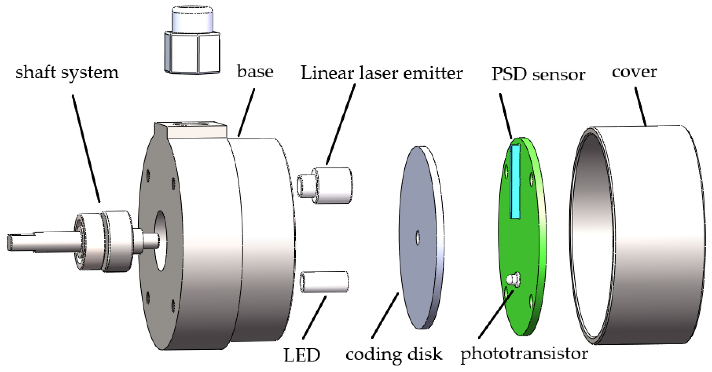
Figure 1 shows the working principle of the photoelectric encoder, which is mainly composed of a linear laser emitter, a coding disk, a photoelectric detection module, a transmission shaft, an LED light source, a photoelectric transistor, and bearings. The photoelectric detection module includes a PSD sensor, a photoelectric transistor, and corresponding signal processing circuits. The length direction of the linear light spot emitted by the linear laser emitter coincides with the length direction of the PSD, and the linear light source is projected onto the PSD sensor through the code disk. The PSD sensor is fixed on the photoelectric detection circuit board, and the electrical signal output by the PSD sensor can be converted into position information through the amplification circuit and detection circuit. The light signal output by the LED is projected onto the photosensitive area of the photoelectric transistor through the inner circle code track of the code disk. The inner circle of the code track is the transparent area within 0°~180° and the non-transparent area within 180°~360°. When the photoelectric transistor does not receive the light signal, it indicates that the PSD measures the angle information within the range of 0°~180°. When the photoelectric transistor receives a light signal, it indicates that the PSD measures angle information within the range of 180°~360°.
In this study, the light transmission area of the code disk adopts a continuous design. When the encoder is working, the code disk rotates with the transmission shaft, and the light sources and photoelectric detection module are stationary. The distance from the geometric center of the light spot projected onto the PSD sensor to the geometric center of the transmission shaft is in a linear one-to-one correspondence with the circumferential angle. Based on the position information output by the PSD sensor, the distance from the light spot to the center of the code disk is calculated, so the angle position information of the encoder is obtained.
2.1. PSD Sensors and Signal Processing Circuits
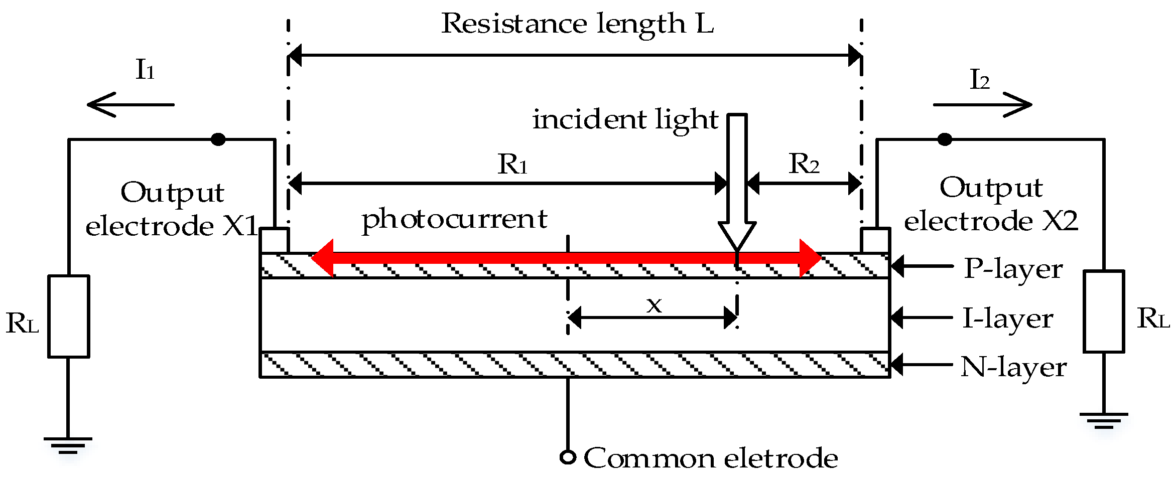
A PSD sensor is a photoelectric device that is sensitive to the position of the center of gravity of the incident light spot on its photosensitive surface. When the incident light spot falls at different positions on the photosensitive surface of the device, the PSD will output different electrical signals accordingly. By processing this output electrical signal, the position of the incident spot on the PSD can be calculated. The intensity and size of the incident light are independent of the position output signal of the PSD, and the position output of the PSD is only related to the position of the center of gravity of the incident light.
The one-dimensional PSD selected in this article is a PIN three-layer structure, with a cross-section shown in
Figure 2. The surface P layer is a photosensitive surface, with two signal output electrodes on each side. The common electrode at the bottom layer is used to apply a reverse bias voltage. When the incident light points illuminate a point on the PSD photosensitive surface, it is assumed that the total photocurrent generated is
I0. Due to the transverse potential between the incident light point and the signal electrode, if a load resistor is connected to the two signal electrodes, the photoelectric current will flow to the two signal electrodes, thus obtaining the photoelectric currents
I1 and
I2 from the signal electrodes. Obviously, the sum of photocurrent
I1 and
I2 is equal to the photocurrent
I0, and the shunt relationship between I
1 and I
2 depends on the equivalent resistance R
1 and R
2 between the incident light point position and the two signal electrodes.
Assuming that the resistance value of the load resistor R
L can be ignored relative to R
1 and R
2,
Here, L is the length of the PSD photosensitive surface, and x is the distance from the incident light point to the midpoint of the PSD. Formula (1) indicates that the ratio of the output photocurrent of two signal electrodes is the reciprocal of the ratio of the distance between the incident light point and the electrode.
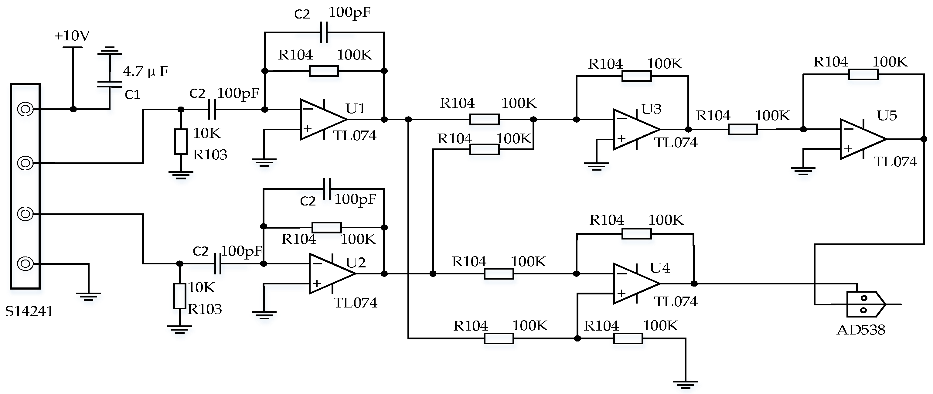
According to Formula (1), the signal processing circuit of the PSD sensor is designed. The circuit schematic is shown in
Figure 3. The photocurrents
I1 and
I2 first pass through low-pass filters U1 and U2 for the removal of high-frequency noise and pulse interference. Then,
I1 + I2 and
I2 −
I1 are obtained through addition and subtraction circuits, respectively, and finally, (
I2 −
I1)/(
I1 + I2) is obtained through division circuits. The division function is implemented using the real-time analog signal calculation unit AD538. AD538 is a single-chip real-time computing circuit that can provide accurate multiplication, division and exponentiation operations for analog signals; the dynamic range of the input signal can be large, the linearity of the output signal is good, and the circuit has the characteristics of low power consumption and high reliability.
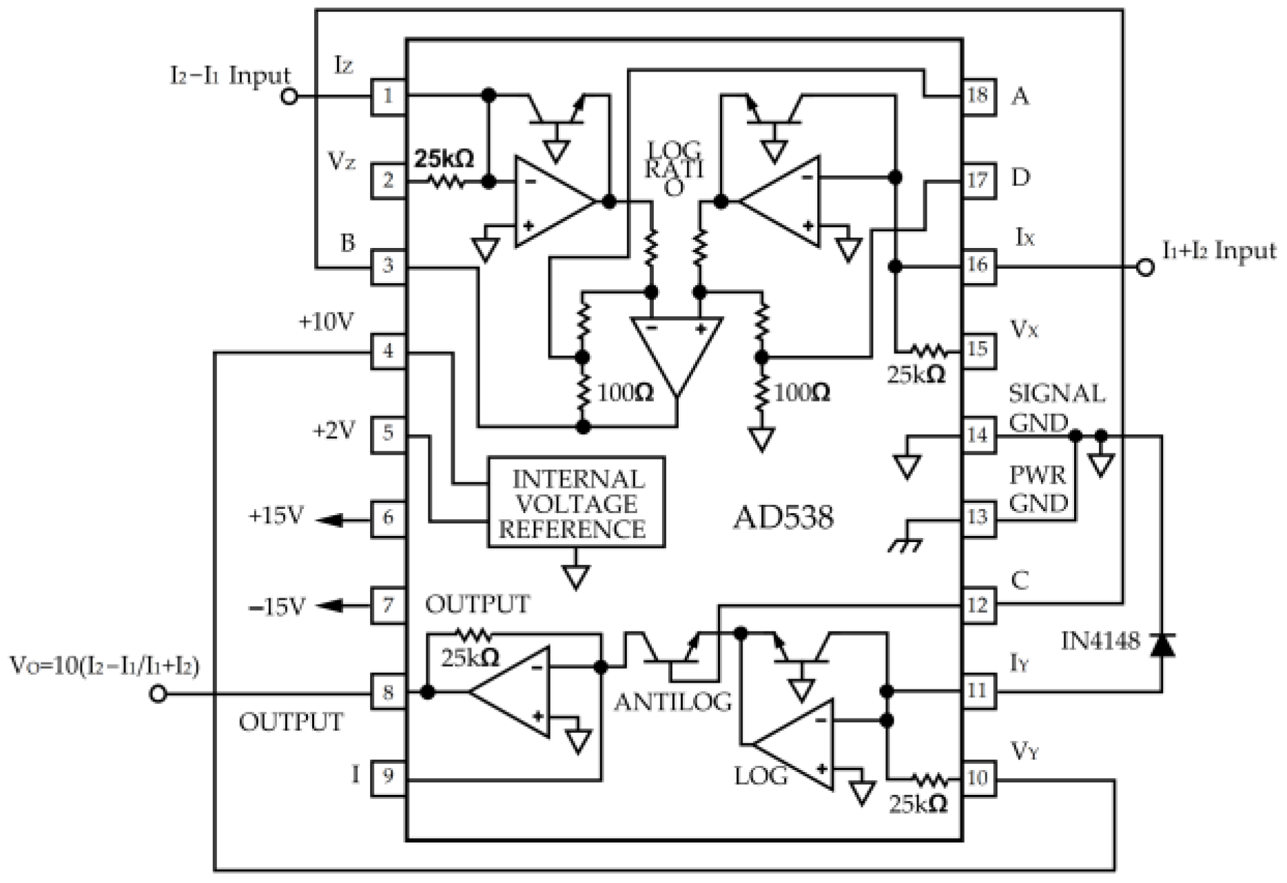
The operation expression of AD538 is V
OUT = V
Y(V
Z/V
X)
m. Depending on different requirements, the external circuit and input signal connection of AD538 can be changed to achieve different operations; this article uses the dual input division operation function of AD538.
Figure 4 shows the line diagram of AD538 performing the V
OUT = 10(V
Z/V
X) operation. As shown in
Figure 4, pins 6 and 7 of AD538 are connected to +15 V and −15 V power supplies, respectively, and pins 14 and 13 are for signal ground and power ground, respectively. The dividend analog signal I
2 − I
1 and the divisor analog signal I
1 + I
2 are connected to pins 1 and 16, respectively. The final output signal of pin 8 is V
OUT = 10(I
2 − I
1/I
1 + I
2). The coefficient 10 in the formula is determined by the V
Y voltage; by adjusting the voltage of pin 10 of AD538, the coefficient can be changed to linearly adjust the final output amplitude.
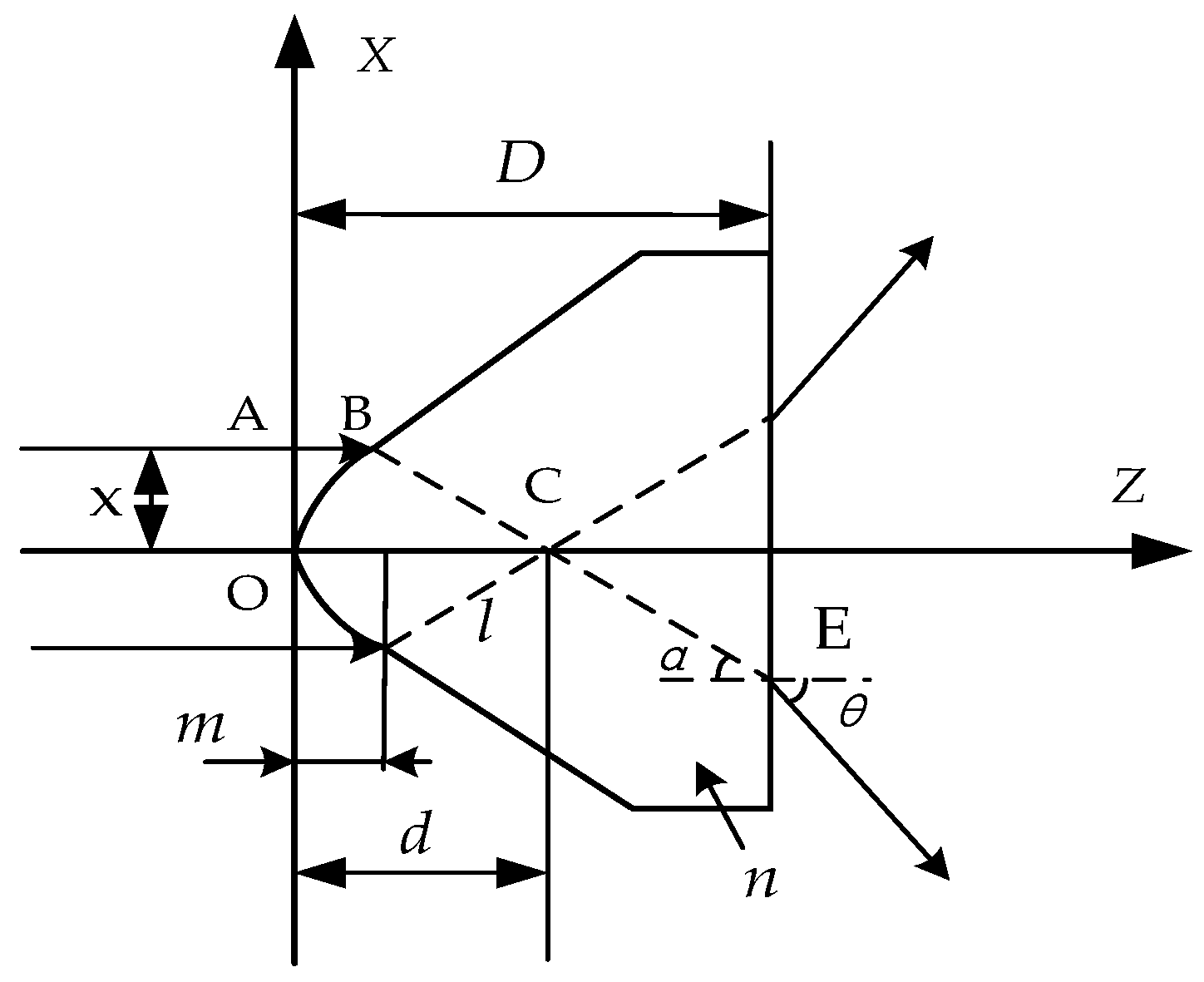
2.2. Design of Code Disk
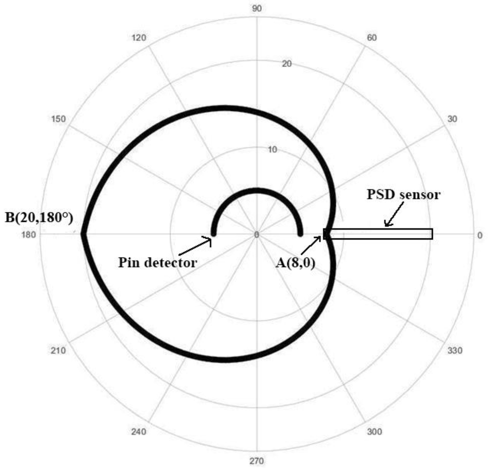
This article uses the principle of photoelectric conversion to convert the circumferential position into the electrical signal of the laser spot on the PSD sensor and photoelectric transistor. As shown in
Figure 5, the code disk contains two circles of code tracks, named the inner circle code track and the outer circle code track; the thick black solid line in
Figure 5 represents the light transmission part. The LED and photoelectric transistor are fixed on the base and circuit board, respectively, and are used to read the information of the inner circle code track. As the code disk rotates, when the output signal of the photoelectric transistor is quantized to 0, it indicates that the outer circle PSD measures angle information within the range of 0°~180°; when the output signal of the photoelectric transistor is quantized to 1, it indicates that the outer circle PSD measures angle information within the range of 180°~360°. To ensure that the center position of the light spot on the PSD sensor varies linearly with the rotation angle within 0°~180° and 180°~360°, the code disk is designed as shown in
Figure 5. A polar coordinate system is established with the center of the code disk as the pole O and OA as the polar axis. The black solid line in the figure represents the part that can be penetrated by light. The coordinates of points A and B are (8, 0°) and (20, 180°), respectively. Within the range of 0°~180° and 180°~360°, the polar coordinates of each point P on the centerline of the transparent part are set as (ρ, θ), and ρ and θ are in a linear relationship, assuming they satisfy the following functional relationships:
Here,
represents the angle value output by the photoelectric encoder,
and
represent the linear proportional coefficients,
and
represent the correction constants,
represents the distance from each point on the center line of the light transmission part of the code disk to the center of the code disk,
represents the high and low levels of the pulse signal output by the phototransistor, and “1” and “0” represent the light transmission area and the non-light transmission area, respectively. When A
1 = 0, by substituting polar coordinates A (8, 0°) and B (20, 180°) into Equation (2), we can obtain
. When A
1 = 1, by substituting A (8, 360°) and B (20, 180°) into Equation (2), we can obtain
, and by substituting them into Equation (3), we can obtain
The one-dimensional position-sensitive detector (PSD) with Hamamatsu’s model of S14241 is selected to receive the laser signal output by the linear laser transmitter. Refer to
Figure 2 for the structure of the one-dimensional position-sensitive detector S14241. According to the conversion Formula (1) of the spot position on the detector, we can obtain
2.3. Design of Linear Light Source
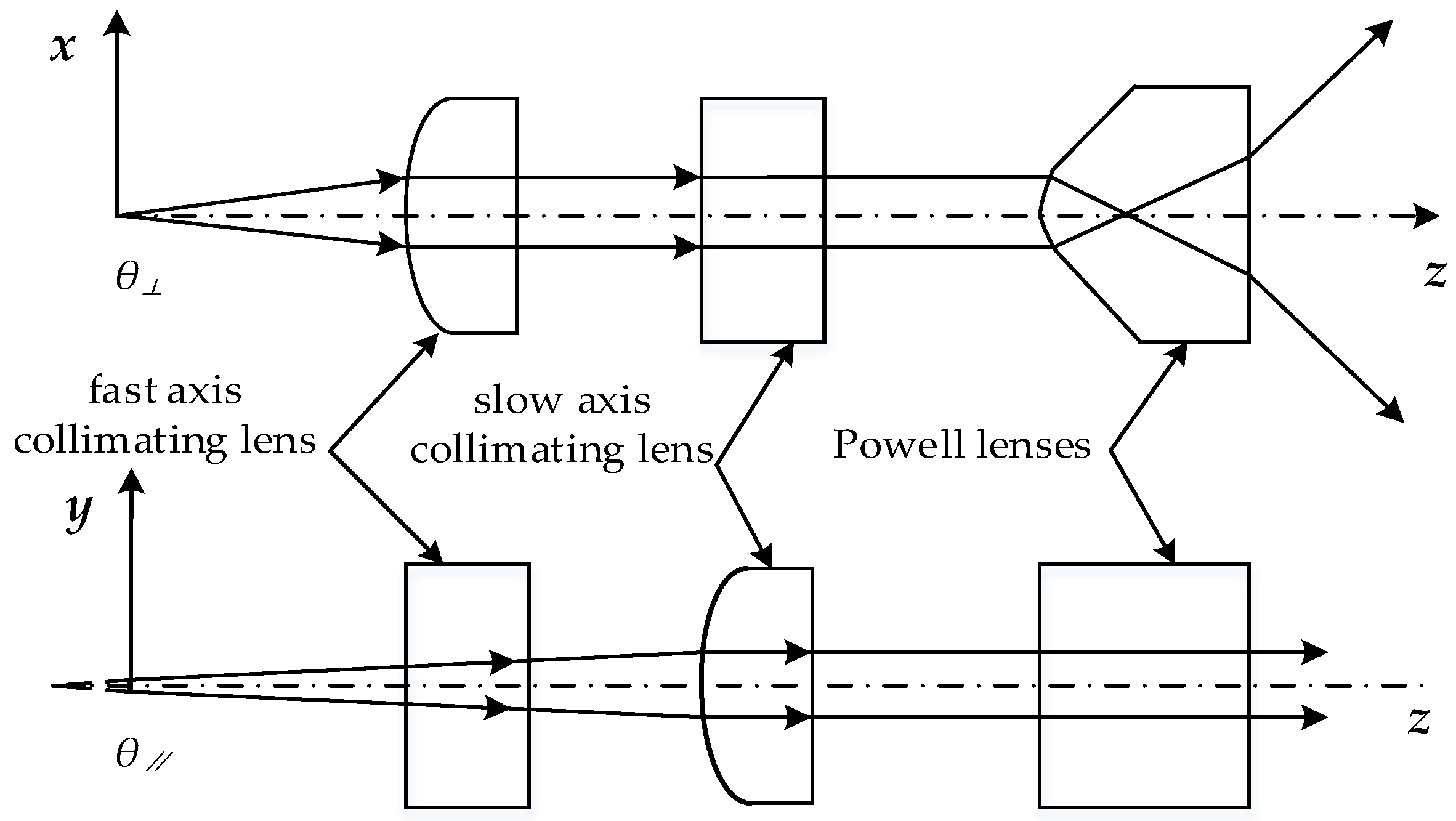
A diode laser is a kind of laser using semiconductor materials as the working material, and its working area is very thin. The outgoing beam is a severely asymmetric elliptical astigmatic beam. The divergence angle in the fast axis direction which is perpendicular to the p-n junction is 30°~40°, and the divergence angle in the slow axis direction which is parallel to the p-n junction is 10°~20°. As shown in
Figure 6, in order to obtain an even straight-line beam, the elliptical beam output by the diode laser passes through two cylindrical lenses in turn to collimate the beam in the fast axis direction and the beam in the slow axis direction and then expands the beam in the fast axis direction through the Powell prism. A Powell prism is an optical line drawing prism, which makes the laser beam output a straight line with even optical density, good stability, and good linearity. At the same time, the Powell prism is better than a cylindrical lens, and it can eliminate the central hot spot and fading edge distribution of a Gaussian beam.
According to the Fraunhofer diffraction effect of the circular hole, the diffraction pattern is an annular stripe, assuming that
θ is the diffraction angle of the first dark stripe and the angular radius of the Airy spot and
r0 is the radius of the Airy spot. The following formulas can be derived:
Here, D is the diameter of the circular hole, is the wavelength of the semiconductor laser, f is the focal length of the lens, r1 is the radius of the output laser of the lens, and the specified diffraction coefficient β is used to measure whether the diffraction effect is obvious. The larger the value β, the weaker the diffraction effect. Generally speaking, when β > 4, the influence of the diffraction effect can be ignored. In the optical design of this paper, the diffraction coefficient of each lens is guaranteed that β > 4. The influence of the diffraction effect can be ignored, and the optical path design of the system can be realized through geometric optical design.
- (1)
Fast axis collimation optical path design
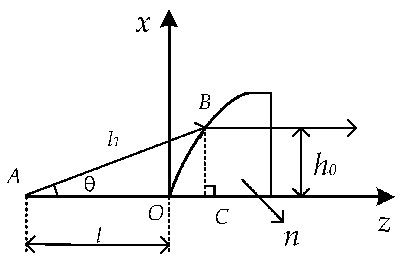
The principle of fast axis collimating optical path is shown in
Figure 7. The aspheric cylindrical lens is used to collimate the beam. In order to reduce the processing difficulty and cost, one surface of the aspheric lens is aspheric and the other surface is planar. Because the dimension perpendicular to the p-n junction direction is about 1 μm, the light source is approximated as a point light source. Assuming that the coordinates of point B are (z, x), the following relationship can be obtained from the refraction theorem of light and the Fermat theorem:
By combining the above two equations, we can obtain
According to the aspheric equation, the surface is a quadric surface, and its curvature and conic coefficient are
In Formula (12), the refractive index n of the lens is related to the material of the lens and the wavelength of the laser. The distance
l between the light source and the top of the lens is related to the divergence angle of the laser and the light height after laser collimation. The following formula can be deduced from
Figure 7:
By combining the above two formulas, it can be obtained that
where
is the radius of the spot output by the fast axis after laser collimation, in which
is half of the fast axis divergence angle of the semiconductor laser diode.
- (2)
Slow axis collimation optical path design
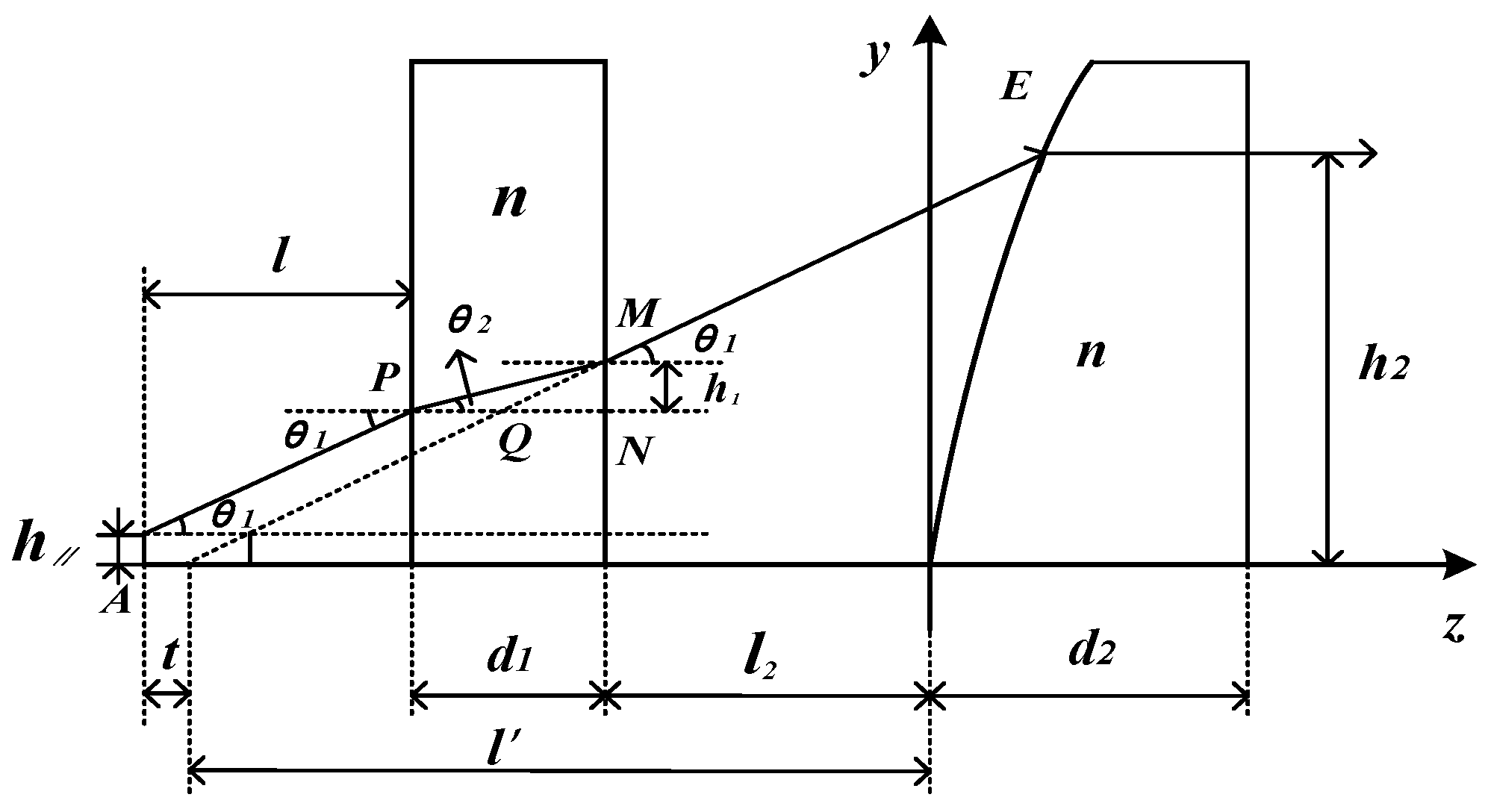
The principle of the slow axis collimating optical path is shown in
Figure 8. The aspheric cylindrical lens is used to collimate the beam. The size parallel to the p-n junction direction is about 10 μm. Therefore, the light source needs to be equivalent to a linear light source. When the light passes through the parallel flat lens, it will produce a horizontal right offset, and its offset is PQ. According to the position relationship in the figure, the following relationship can be obtained:
According to the above formulas, we can obtain
As shown in
Figure 8, in the slow axis direction, due to the inherent astigmatism of the semiconductor laser, the focus of the aspheric lens is not at the same point in both directions of the fast axis and the slow axis, and assuming that the distance of the focus in both directions is t, according to the divergence angle of the semiconductor laser and the size of the active layer, the following formulas can be obtained:
Here,
=
μm, and
is the half angle of the slow axis divergence angle. According to the aspherical Equation (11) of the fast axis, similarly, the following can be obtained:
According to the aspherical equation, the surface is a quadratic surface, with curvature and conicity coefficients as follows:
From Formula (15), the following can be deduced in the same way:
where
is the radius of the spot output from the slow axis after laser collimation and
is half of the divergence angle of the slow axis of the semiconductor laser diode.
- (3)
Design of Powell prism
The beam expansion principle of the Powell prism is shown in
Figure 9. When the collimated laser beam is incident on the arc-shaped edge OB of the Powell prism, the diameter of the outgoing beam in this direction is equal to the effective width on the image plane, which is equivalent to the rapid focusing of the beam in a single direction, resulting in an increase in the divergence angle of the beam. The refraction angle is mainly determined by the angle between the two edges and finally refracts again when passing through the outgoing surface. The whole outgoing light forms a fan-shaped beam, which has the effect of linear beam expansion on the image plane.
The incident parallel light from A to C and light from O to B meet the Fermat principle that the optical paths are equal. Assuming that the coordinates of point B are (z, x), the following expression is derived:
where n is the refractive index of Powell prism and the refractive index of air is 1. The coefficients of the aspheric equation are obtained as follows:
The exit angle of Powell prism θ meets the refraction law:
The angle α between the light and the optical axis in the Powell prism meets the following relationship:
Here, the radius x of the incident spot, the divergence angle θ after emission, and the refractive index n of the lens are known parameters. The parameters of the Powell prism can be calculated according to the above formulas, and then the parameters of the radius and thickness of the Powell prism can be calculated according to some constraints.
3. Simulation and Analysis
In this paper, the semiconductor laser HL6362MG of Thorlabs company is selected as the light source, and its performance parameters are shown in
Table 1. This 640 nm, 40 mW TO packaged laser diode is a compact light source that outputs a single transverse mode and is suited for a variety of applications such as a laser display, laser scanner, or light source for optical equipment. The refractive index for air is n = 1; for glass BK7 medium, it is n = 1.5148.
According to the mathematical model of semiconductor LD, the parameters in the mathematical model of a collimating optical path are calculated by Matlab R2021a software. The calculation results are shown in
Table 2. According to the data in
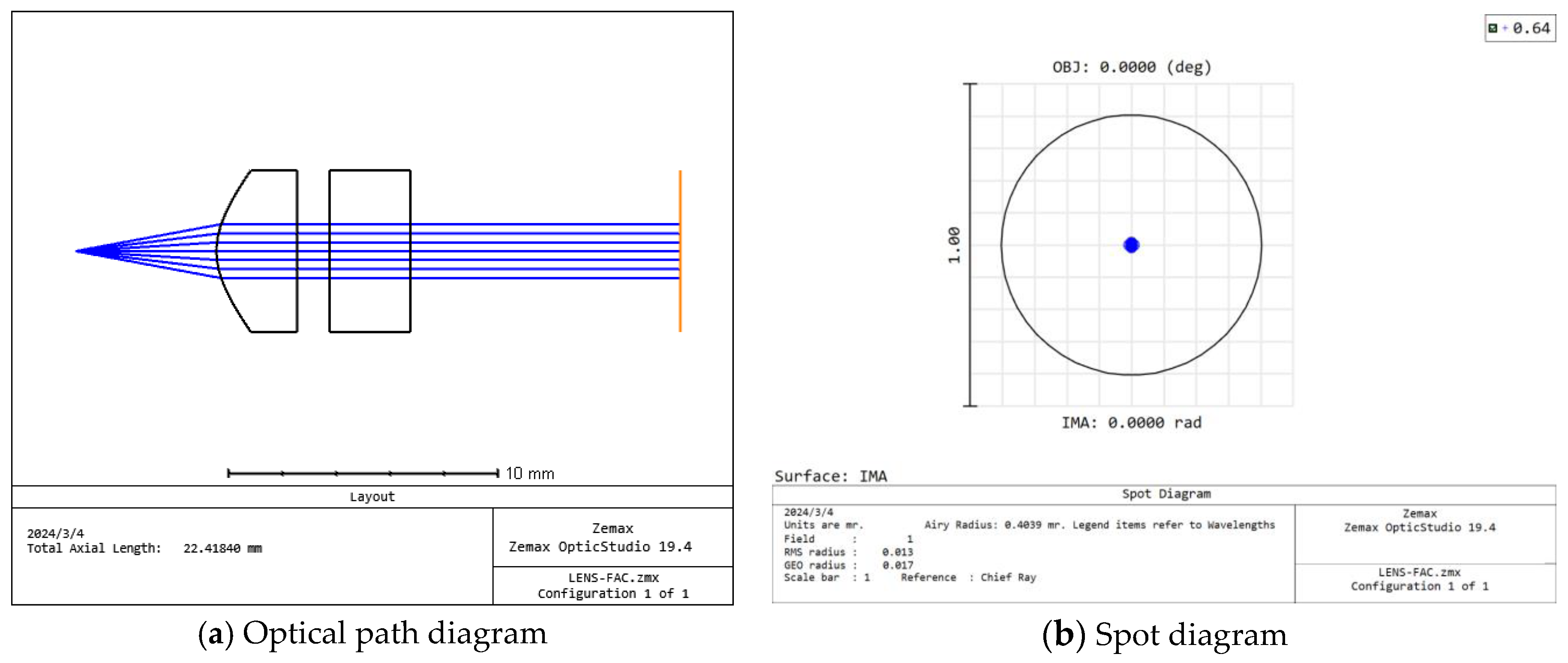
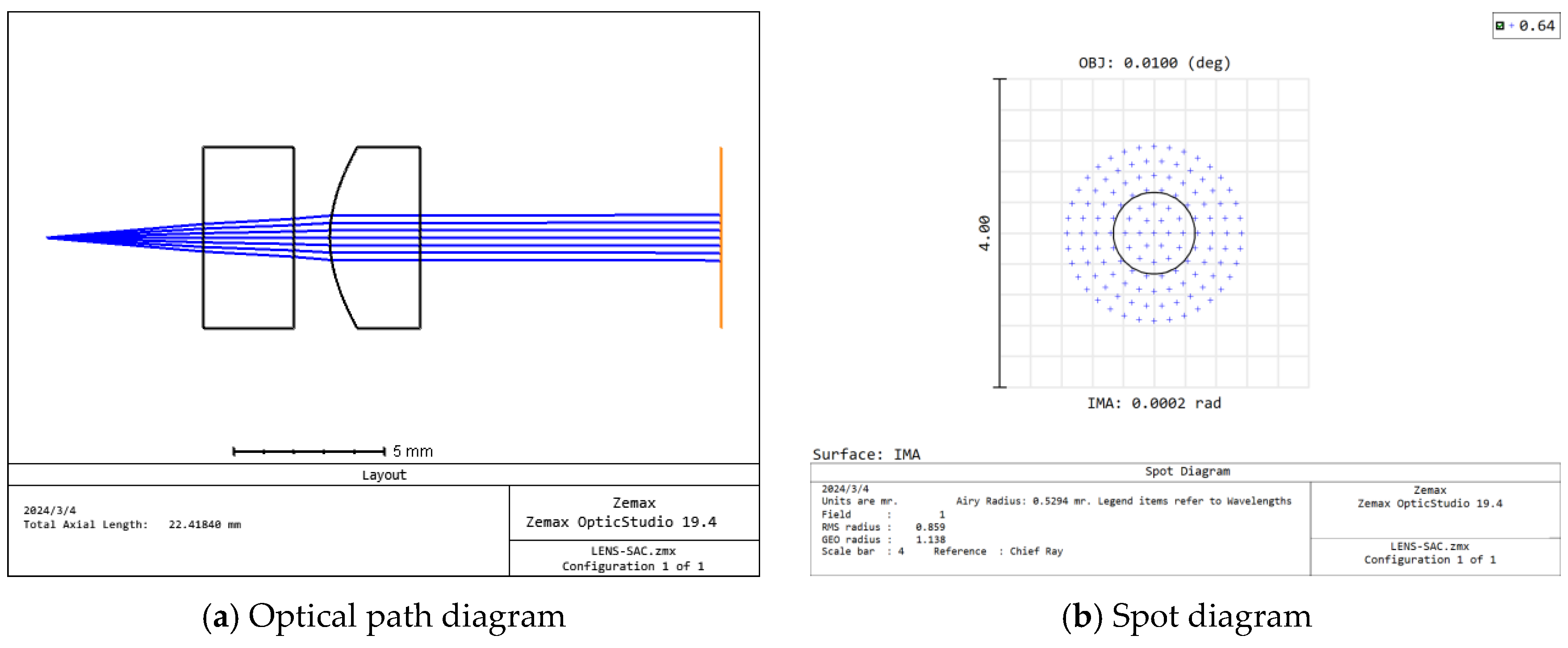
Table 2, the optical path was simulated by Zemax OpticStudio 19.4 software. In
Figure 10 and
Figure 11, after collimation, the divergence angles of the fast axis and slow axis are 0.013 mrad and 0.859 mrad, respectively. It can be seen from the point diagram that the RMS radius is less than or close to the radius of Airy spot, and the system has reached or is close to the diffraction limit.
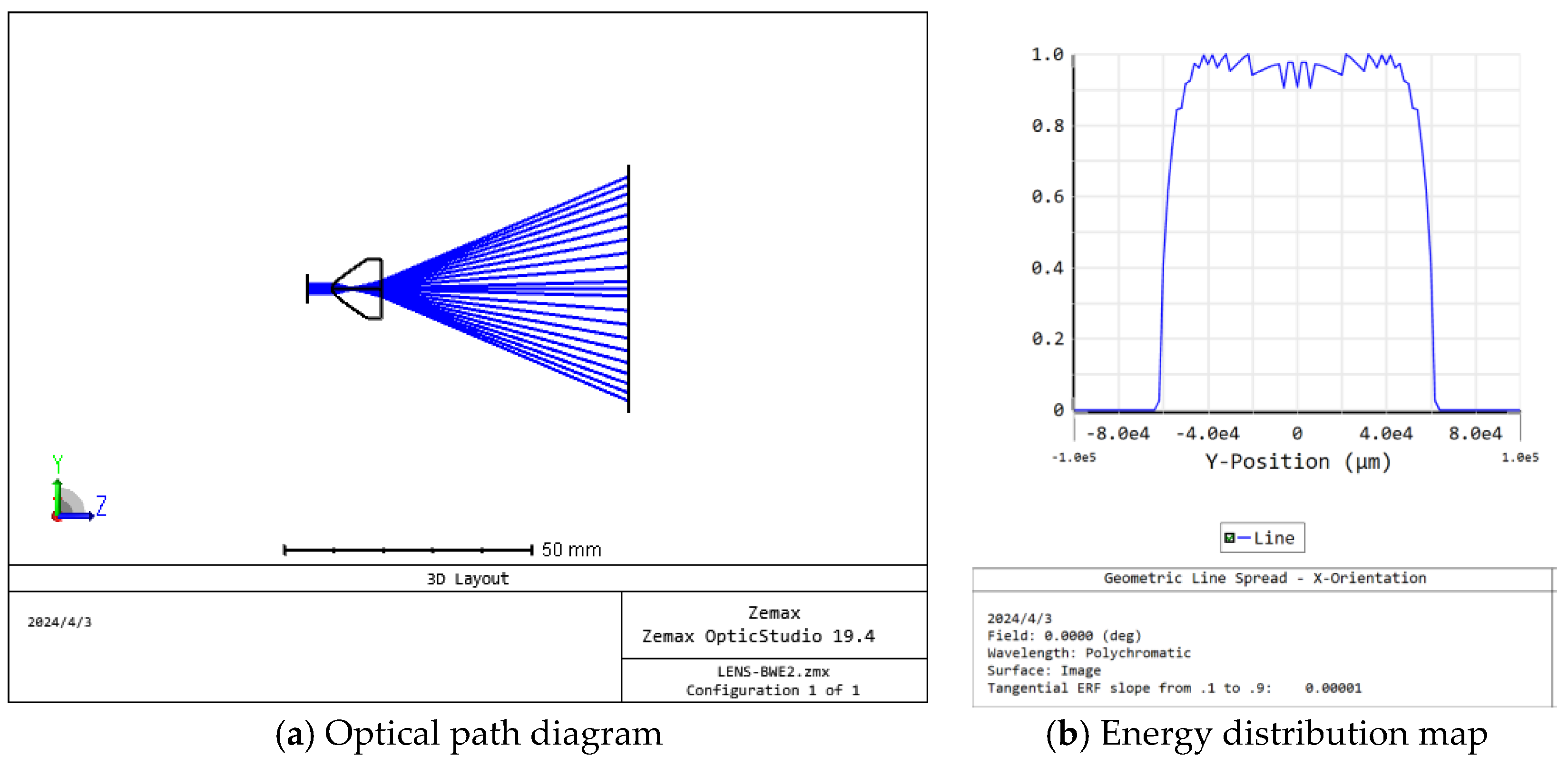
One of the main applications of the Powell prism is to transform the fundamental mode Gaussian beam into a linear light spot. In order to observe the shape and uniformity of the linear light spot, Zemax OpticStudio 19.4 software was used to simulate it in nonsequential mode. The 3D light path structure diagram is shown in
Figure 12a. After passing through the Powell prism, the light only diverges rapidly in the vertical direction but remains unchanged in the parallel direction, and the length of the light spot projected by a linear laser onto the photosensitive surface of the PSD is 12 mm. The light intensity distribution after shaping is shown in
Figure 12b. The incident light source is an oval spot with Gaussian distribution, which is shaped into an even one-line spot.
4. Encoder Test and Calibration
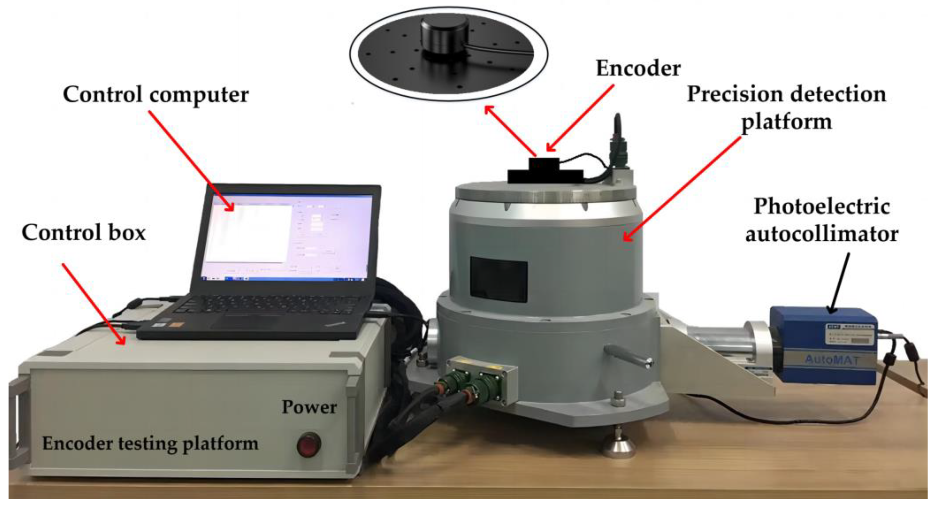
On the basis of the above principles and simulation analysis, a prototype of the encoder was designed and manufactured, with external dimensions as follows: Φ50 mm × 30 mm, with a resolution of 18 bits. The direct comparison method was used for accuracy detection; the principle is shown in
Figure 13. The autocollimator and the regular polyhedron are used to form an optical position closed loop as the angle reference; the fixed position optical reflection device is also installed to detect the signal drift of the autocollimator in the process. The performance of the testing equipment is ±360° continuous or compensated testing, and the internal and external biaxial structure is adopted. The positioning accuracy of the internal and external axis angular position is ±0.2″, the angular position stability is ±0.36″, the perpendicularity and axis rotation accuracy of the axis system is ≤±2″, and the angular positioning resolution is ≤0.36″. The detection equipment is composed of a rapid detection platform and a control box, which can transmit the collected data to the host for display within the displayed time period. The readings of the encoder and the detection equipment are directly compared to calculate the angle measurement error of the instrument, and some of the detection data are shown in
Table 3.
The angle measurement error can be used as standard deviation σ, and the standard deviation is calculated as follows:
where
is the measured value,
is the random error, and
is the arithmetic mean of measured values. According to Formula (29), the measurement error
of the photoelectric encoder is 0.78′, and the measurement accuracy of the photoelectric encoder is about 0.78′.
The errors are classified based on the sources of errors generated during the encoder design process. The encoder errors include theoretical errors, encoder disk engraving errors, PSD sensor measurement errors and shafting errors, and installation and debugging errors. The nonlinearity of the PSD often presents a slow gradient change and has the characteristics of uncertainty, which directly affects the measurement accuracy of the whole measurement system, so its nonlinear error must be corrected.
In the photoelectric encoder, the position error corresponding to the one-dimensional PSD in the X direction in
Figure 2 is linearly converted into the angular error of the encoder. Due to the non-uniformity of the PSD material, this position error will show a gradient change with a relatively slow change. Through the photoelectric encoder detection platform, a group of angle data (
) are measured, where
represents the measured value of the angle,
represents the actual value of the angle, and the angle error
, so a group of discrete photoelectric encoder angle error data (
) can be obtained. In order to study the variation character of the angle error at any angle, it is necessary to calculate the function according to this set of numbers, so that the function can pass through or approach all nodes A
i (
) as much as possible.
In order to correct the nonlinear error of the PSD sensor, this paper adopts the cubic spline interpolation method to compensate for the angle measurement value of the photoelectric encoder. Using the cubic spline function as an interpolation function will not cause the Runge phenomenon, and the interpolation effect is significantly better than using polynomial interpolation. In order to improve the accuracy of interpolation, when using the spline function as interpolation, we can use the method of adding interpolation nodes. When using a polynomial as an interpolation function, adding interpolation nodes will inevitably increase the degree of the polynomial, which often causes numerical instability.
The function of cubic spline interpolation is defined as follows:
Each node on the fixed interval [a, b], and function value , if s(x) meets the following:
- (1)
;
- (2)
S(x) is a polynomial of degree less than or equal to 3 in each interval ;
- (3)
S(x), S′(x), S″(x) is continuous on [a, b].
Then s(x) is called the cubic spline interpolation function of function f(x) with respect to nodes 0, 1, …, n.
Assuming that the angle is
, the second derivative
of the cubic spline function S(t) on the interval
is equal to
; because S(t) is a cubic polynomial on the interval
, then S″(t) is a linear function on the interval, which can be expressed as
where
is a pending parameter,
.
By integrating
twice, we can obtain
From the known condition
, we can determine the integral constant
,
:
Taking
into
and performing derivitization, we can obtain
Similarly, for
,
Then, according to the continuity of the first derivative, we can obtain
where
,
is the second-order difference quotient of
at point
. Equation (36) represents n − 1 equations containing n + 1 unknown parameters
(i = 0, 1, 2, … …, n). In order to solve
uniquely, the boundary condition
= 0 is supplemented. In this way,
can be obtained, and then the cubic spline function
on the interval
can be obtained.
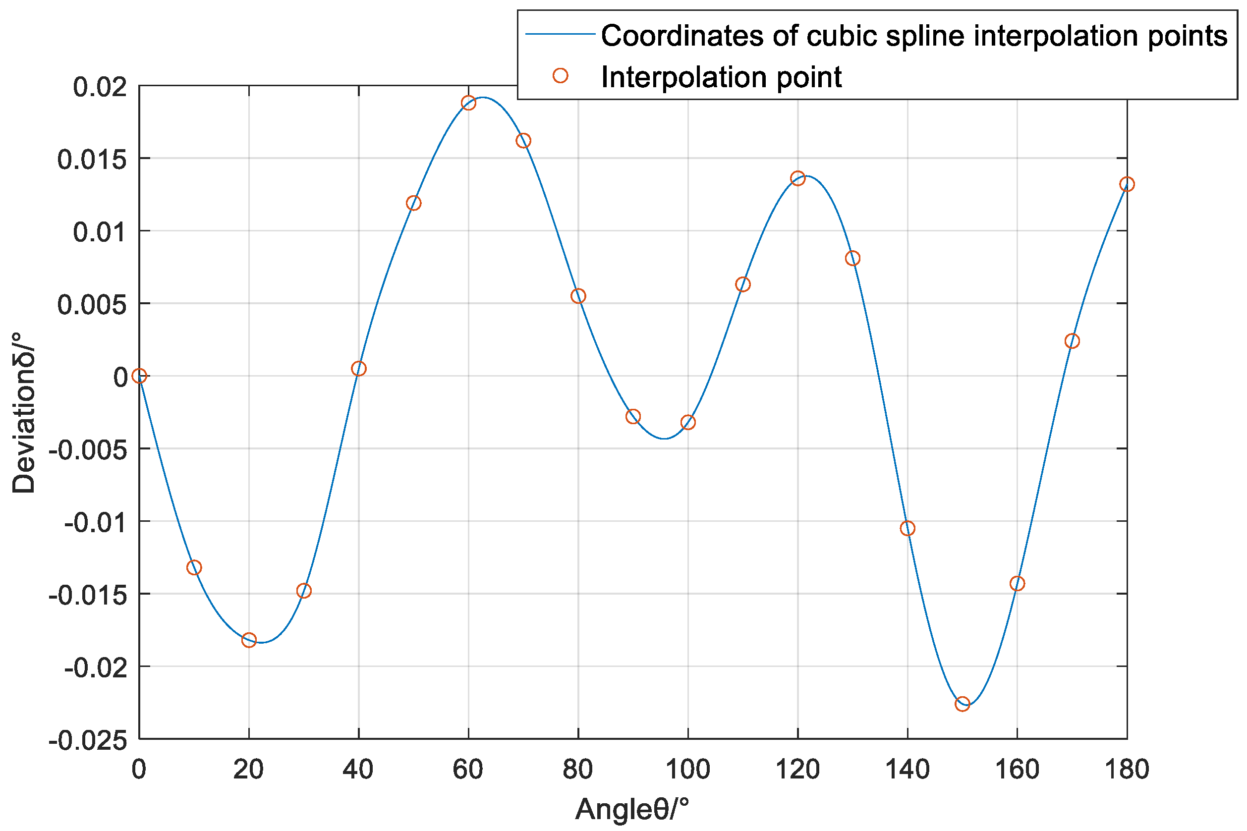
Based on the above principle, the PSD sensor was calibrated by Matlab R2021a software. According to the 19 groups of data (
) provided in
Table 3, taking the interval [0°, 180°] as an example, cubic spline interpolation is performed. The interpolation function image is shown in
Figure 14. The measurement error of the PSD sensor is the smallest in the middle area and gradually increases on both sides. The measurement error of each measurement point after the photoelectric encoder is calibrated by cubic spline interpolation compensation is shown in
Table 4. After calculation, the measurement accuracy of the photoelectric encoder is about 5.4″.
5. Conclusions and Prospect
Aiming at the industrialization and engineering problems of photoelectric encoders, a new type of absolute photoelectric encoder is proposed. The linear light source, encoding and decoding method, and calibration method of the encoder are designed. The designed encoder is tested, and the results show that the measurement accuracy can reach 5.4″ (1σ). Compared with the traditional photoelectric encoder, the measurement method is simple and easy to implement, which further shows that the principle and method proposed in this paper are feasible, which is of great significance for improving the measurement accuracy and industrialization of encoders.
The photoelectric rotary encoder is developing in the direction of changing the measurement method. With the maturity and application of relevant machine vision algorithms, the rotary encoder will further simplify the optical system and reduce the size of rotating parts in the mechanical system in the future. The core device will change from the code disk to the image sensor and subsequent circuits, and the measurement resolution and final accuracy will be more dependent on the quality of subsequent processing algorithms. At the same time, the response speed of the encoder not only depends on the complexity of the algorithm, but also is closely related to the conversion time of the high-speed AD converter.


