
Simple Modeling and Analysis of Total Ionizing Dose Effects on Radio-Frequency Low-Noise Amplifiers
 , , ,
, , ,
Abstract
:1. Introduction
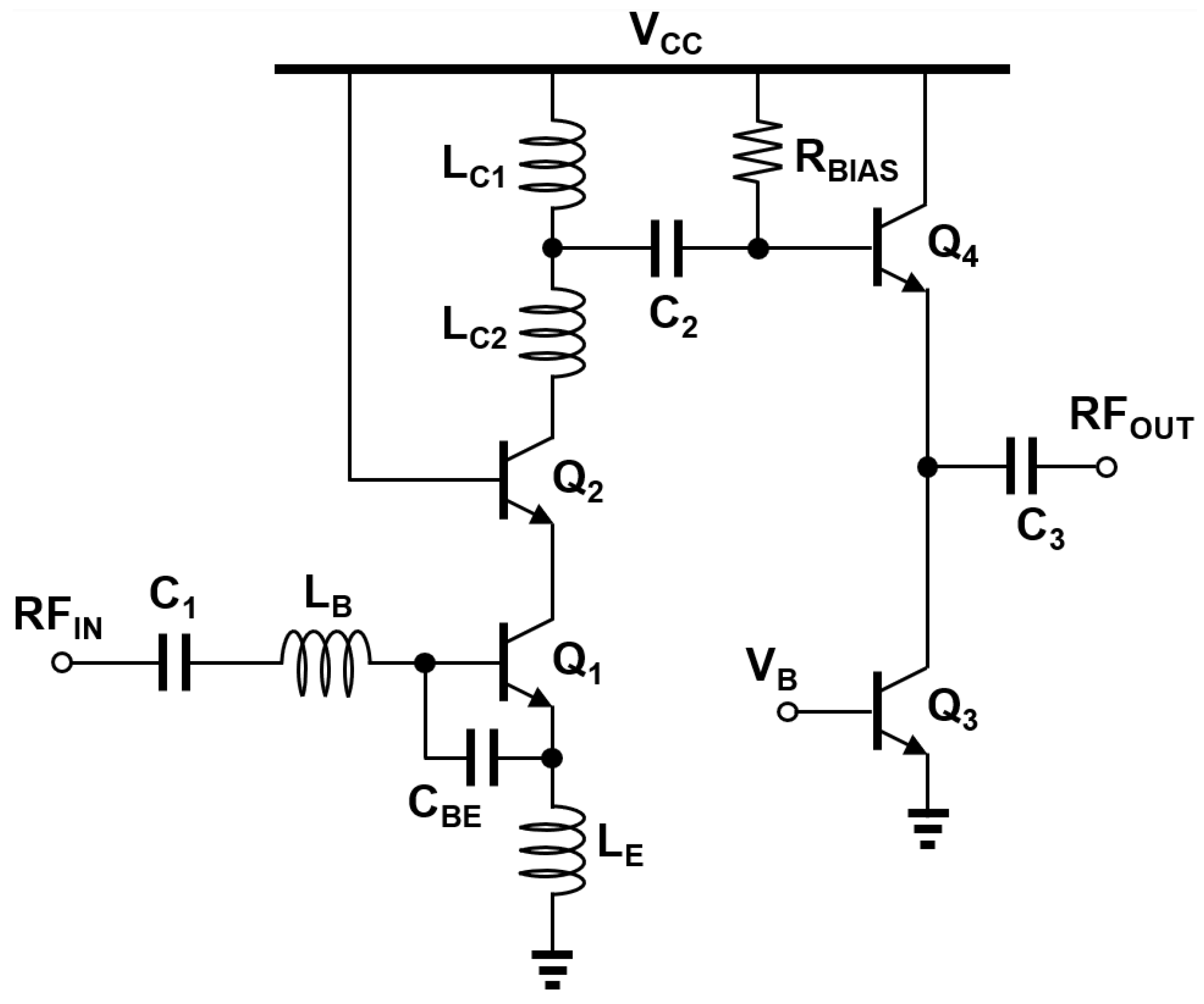
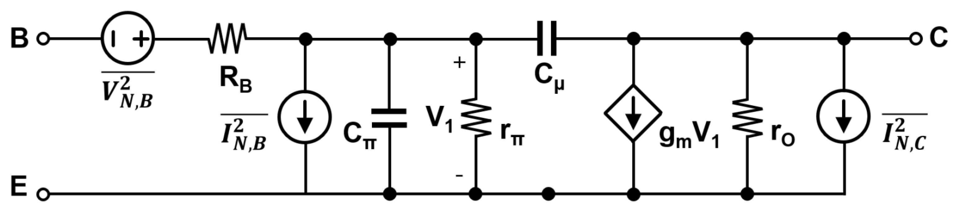
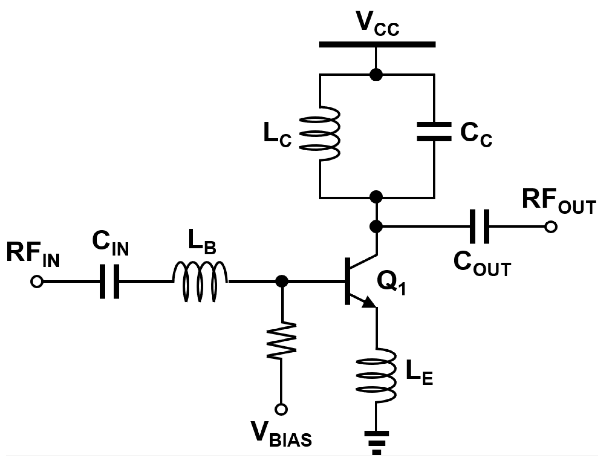
2. LNA Schematic and Device Modeling
3. Experimental Results
3.1. Test Setup for Performance Measurement
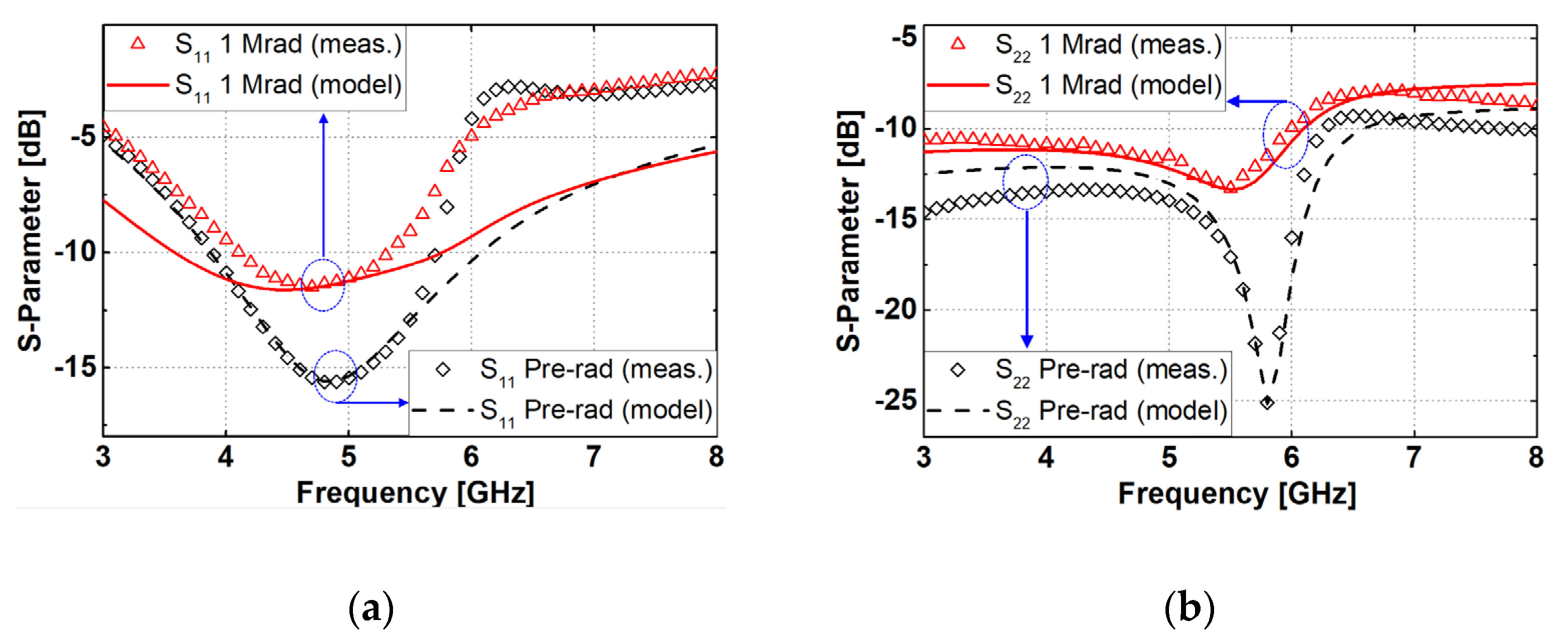
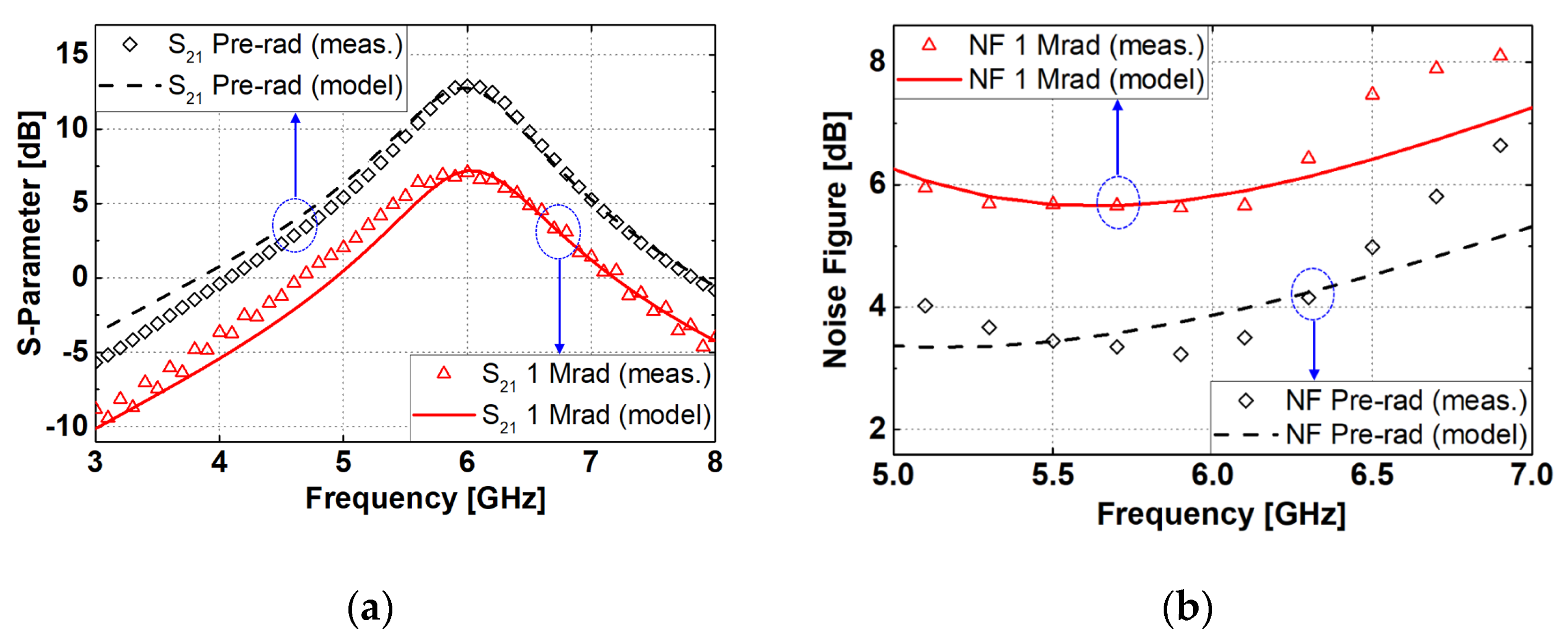
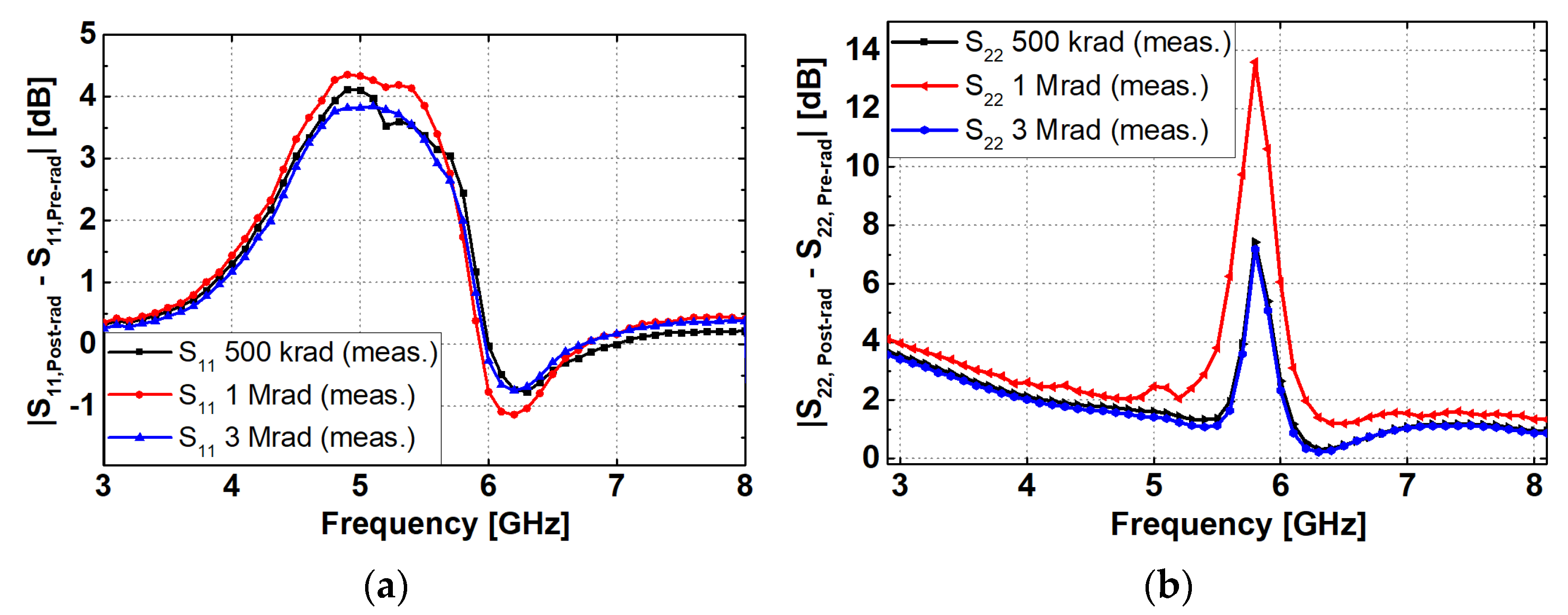
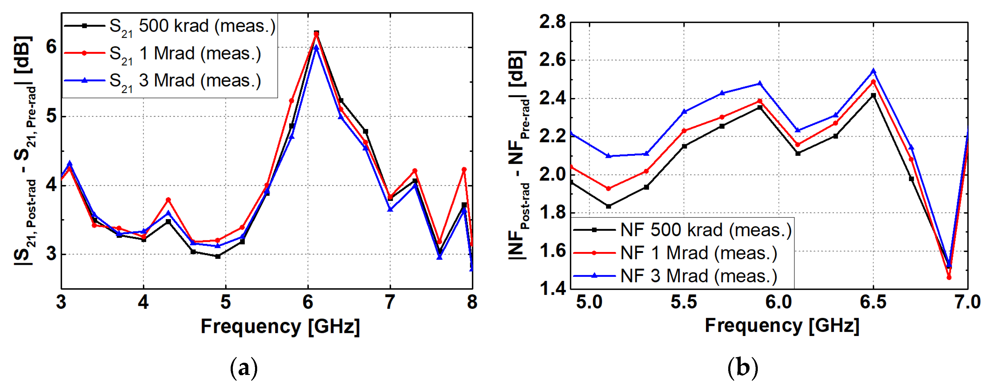
3.2. Performance Degradation and Small-Signal Modeling
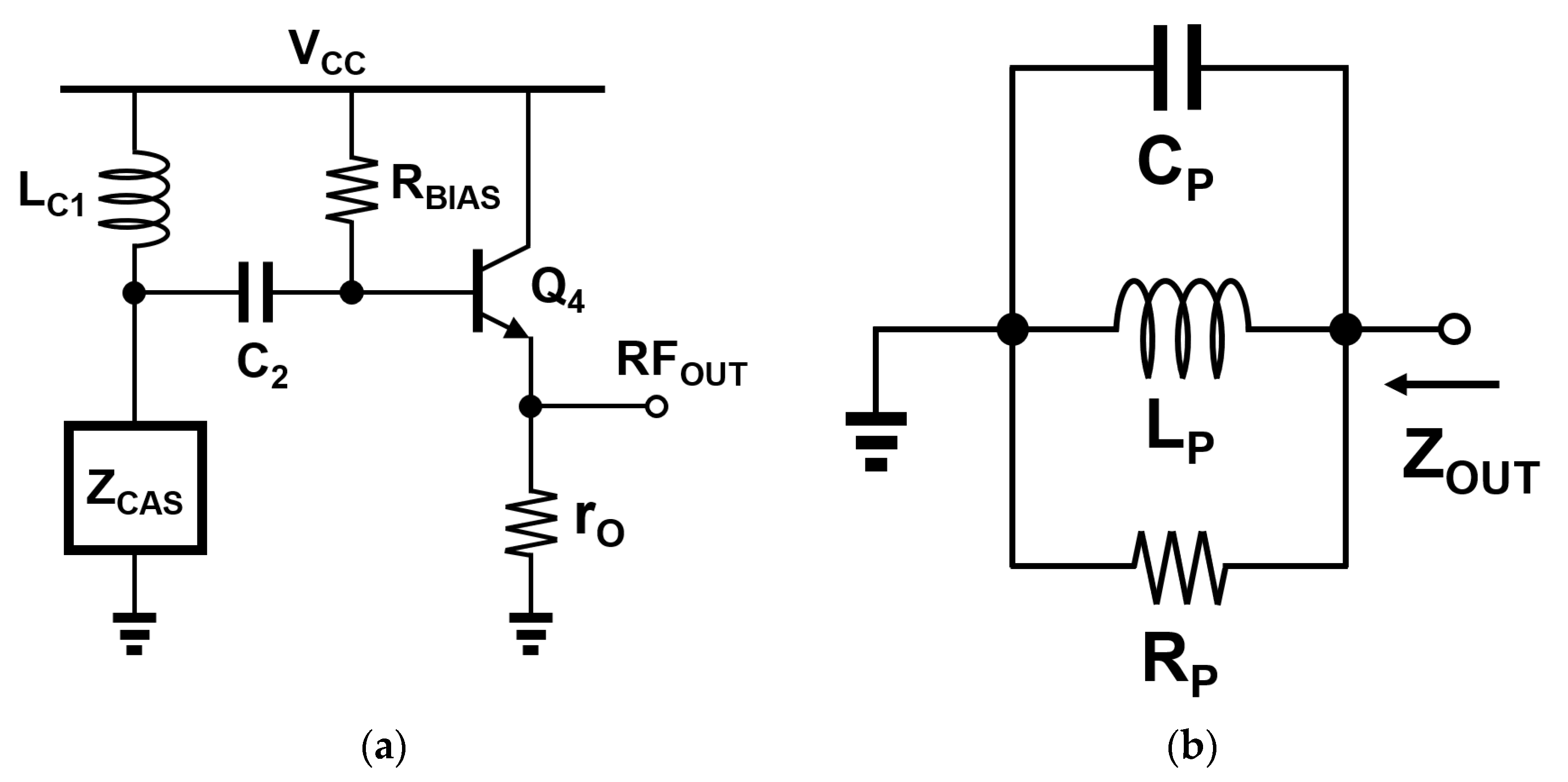
4. Degradation Modeling and Analysis
5. Application to Another LNA Example
6. Summary
Author Contributions
Funding
Data Availability Statement
Conflicts of Interest
References
- Kanar, T.; Rebeiz, G.M. X- and K-band SiGe HBT LNAs with 1.2- and 2.2-dB mean noise figures. IEEE Trans. Microw. Theory Tech. 2014, 62, 2381–2389. [Google Scholar] [CrossRef]
- Song, I.; Cardoso, A.S.; Ying, H.; Cho, M.-K.; Cressler, J.D. Cryogenic characterization of RF low-noise amplifiers utilizing inverse-mode SiGe HBTs for extreme environment applications. IEEE Trans. Device Mater. Reliab. 2018, 18, 613–619. [Google Scholar] [CrossRef]
- Cressler, J.D. Radiation Effects in SiGe Technology. IEEE Trans. Nucl. Sci. 2013, 60, 1992–2014. [Google Scholar] [CrossRef]
- Li, Z.; Liu, S.; Ren, X.; Adekoya, M.A.; Zhang, J.; Liu, S. Experimental investigation on the degradation of SiGe LNAs under different bias conditions induced by 3 MeV proton irradiation. Nucl. Eng. Technol. 2022, 54, 661–665. [Google Scholar] [CrossRef]
- Wei, J.; He, C.; Zhang, P.; Fu, X.; Guo, H.; Luo, T. Impact of Ge profile on TID susceptibility of SiGe HBTs. In Proceedings of the 2021 4th International Conference on Radiation Effects of Electronic Devices (ICREED), Xi’an, China, 26–29 May 2021. [Google Scholar] [CrossRef]
- Ullan, M.; Diez, S.; Campabadal, F.; Lozano, M.; Pellegrini, G.; Knoll, D.; Heinemann, B. Gamma radiation effects on different varieties of SiGe:C HBT technologies. IEEE Trans. Nucl. Sci. 2007, 54, 989–993. [Google Scholar] [CrossRef]
- Zhang, J.X.; Guo, Q.; Guo, H.-X.; Lu, W.; He, C.-H.; Wang, X.; Li, P.; Lin, W. Investigation of enhanced low dose rate sensitivity in SiGe HBTs by 60Co γ irradiation under different biases. Microelectron. Reliab. 2018, 84, 105–111. [Google Scholar] [CrossRef]
- Petrosyants, K.O.; Kozhukhov, M.V. Physical TCAD Model for Proton Radiation Effects in SiGe HBTs. IEEE Trans. Nucl. Sci. 2016, 63, 2016–2021. [Google Scholar] [CrossRef]
- Lerdworatawee, J.; Namgoong, W. Wide-band CMOS cascode low-noise amplifier design based on source degeneration topology. IEEE Trans. Circuits Syst. I Reg. Papers 2005, 52, 2327–2334. [Google Scholar] [CrossRef]
- Li, Z.; Liu, S.; Adekoya, M.A.; Ren, X.; Zhang, J.; Liu, S.; Li, L. Radiation response of SiGe low noise amplifier irradiated with different energy protons. Microelectron. Reliab. 2021, 127, 114396. [Google Scholar] [CrossRef]
- Sarker, M.A.R.; Jung, S.; Ildefonso, A.; Khachatrian, A.; Buchner, S.P.; McMorrow, D.; Paki, P.; Cressler, J.D.; Song, I. Mitigation of single-event effects in SiGe-HBT current-mode logic circuits. Sensors 2020, 20, 2581. [Google Scholar] [CrossRef] [PubMed]
- Zhang, J.; Guo, Q.; Guo, H.; Lu, W.; He, C.; Wang, X.; Li, P.; Liu, M. Impact of bias conditions on total ionizing dose effects of 60Coγ in SiGe HBT. IEEE Trans. Nucl. Sci. 2016, 63, 1251–1258. [Google Scholar] [CrossRef]
- Minko, F.S.; Stander, T. Effect of TID electronradiation on SiGe BiCMOS LNAs at V-band. Microelectron. Reliab. 2020, 112, 113750. [Google Scholar] [CrossRef]
- Mossawir, B.; Linscott, I.R.; Inan, U.S.; Roeder, J.L.; Osborn, J.V.; Witczak, S.C.; King, E.E.; LaLumondiere, S.D. A TID and SEE radiation-hardened, wideband, low-noise amplifier. IEEE Trans. Nucl. Sci. 2006, 53, 3439–3448. [Google Scholar] [CrossRef]
- Fu, X.; You, D.; Wang, X.; Wang, Y.; Mayeda, C.J.; Gao, Y.; Zhang, Y.; Sakamaki, J.; Fadila, A.A.; Li, Z.; et al. A low-power 256-element Ka-band CMOS phased-array receiver with on-chip distributed radiation sensors for small satellite constellations. IEEE J. Solid-State Circuits 2023, 58, 3380–3395. [Google Scholar] [CrossRef]
- Kobal, E.; Siriburanon, T.; Staszewski, R.B.; Zhu, A. A compact, low-power, low-NF, millimeter-wave cascode LNA with magnetic coupling feedback in 22-nm FD-SOI CMOS for 5G applications. IEEE Trans. Circuits Syst. II Exp. Briefs 2023, 70, 1331–1335. [Google Scholar] [CrossRef]
- Jia, X.; Niu, G. Impact of correlated RF noise on SiGe HBT noise parameters and LNA design implications. IEEE Trans. Electron Devices 2014, 61, 2324–2331. [Google Scholar] [CrossRef]
- Weinreb, S.; Bardin, J.C.; Mani, H. Design of cryogenic SiGe low-noise amplifiers. IEEE Trans. Microw. Theory Tech. 2007, 55, 2306–2312. [Google Scholar] [CrossRef]
- Fan, X.; Zhang, H.; Sánchez-Sinencio, E. A noise reduction and linearity improvement technique for a differential cascode LNA. IEEE J. Solid-State Circuits 2008, 43, 588–599. [Google Scholar] [CrossRef]
- Bimana, A.; Sinha, S. Impact of SiGe HBT parameters to the performance of LNAs for highly sensitive SKA receivers. In Proceedings of the 2013 23rd International Conference Radioelektronika (RADIOELEKTRONIKA), Pardubice, Czech Republic, 16–17 April 2013. [Google Scholar] [CrossRef]
- Shaeffer, D.K.; Lee, T.H. A 1.5-V, 1.5-GHz CMOS low noise amplifier. IEEE J. Solid-State Circuits 1997, 32, 745–759. [Google Scholar] [CrossRef]
- Song, I.; Ryu, G.; Jung, S.H.; Cressler, J.D.; Cho, M.-K. Wideband SiGe-HBT low-noise amplifier with resistive feedback and shunt peaking. Sensors 2023, 23, 6745. [Google Scholar] [CrossRef]
- Lee, S.; Ryum, B.R.; Kang, S.W. A new parameter extraction technique for small-signal equivalent circuit of polysilicon emitter bipolar transistors. IEEE Trans. Electron Devices 1994, 41, 233–238. [Google Scholar] [CrossRef]
- Sarker, M.A.R.; Song, I. Design and analysis of fT-doubler-based RF amplifiers in SiGe HBT technology. Electronics 2020, 9, 772. [Google Scholar] [CrossRef]
- Sun, Y.; Fu, J.; Wang, Y.; Zhou, W.; Zang, W.; Liu, J. Direct analytical parameter extraction for SiGe HBTs T-topology small-signal equivalent circuit. Superlattices Microstruct. 2016, 94, 223–230. [Google Scholar] [CrossRef]
- Lee, K.; Choi, K.; Kook, S.H.; Cho, D.H.; Park, K.W.; Kim, B. Direct parameter extraction of SiGe HBTs for the VBIC bipolar compact model. IEEE Trans. Electron Devices 2005, 52, 375–384. [Google Scholar] [CrossRef]
- SiGe Power Amplifier Platforms. Available online: http://gf.com/wp-content/uploads/2021/12/GF21-SiGe-PA-0705.pdf (accessed on 16 February 2024).
- Sirohi, S.; Sirohi, S.; Jain, V.; Raman, A.; Nukala, B.; Veeramani, E.; Adkisson, J.W.; Joseph, A. impact of emitter width scaling on performance and ruggedness of SiGe HBTs for PA applications. In Proceedings of the 2018 IEEE BiCMOS and Compound Semiconductor Integrated Circuits and Technology Symposium (BCICTS), San Diego, CA, USA, 15–17 October 2018. [Google Scholar] [CrossRef]
- Song, I.; Cho, M.K.; Lourenco, N.E.; Fleetwood, Z.E.; Jung, S.; Roche, N.J.-H.; Khachatrian, A.; Buchner, S.P.; McMorrow, D.; Paki, P.; et al. The use of inverse-mode SiGe HBTs as active gain stages in low-noise amplifiers for the mitigation of single-event transients. IEEE Trans. Nucl. Sci. 2017, 64, 359–366. [Google Scholar] [CrossRef]
- Gorchichko, M.; Cao, Y.; Zhang, E.X.; Yan, D.; Gong, H.; Zhao, S.E.; Wang, P.; Jiang, R.; Liang, C.; Fleetwood, D.M.; et al. Total-ionizing-dose effects and low-frequency noise in 30-nm gate-length bulk and SOI FinFETs With SiO2/HfO2 gate dielectrics. IEEE Trans. Nucl. Sci. 2020, 67, 245–252. [Google Scholar] [CrossRef]
- Lambert, D.; Gaillardin, M.; Raine, M.; Paillet, P.; Duhamel, O.; Marcandella, C.; Martinez, M.; Rostand, N.; Lagutère, T.; Aubert, D.; et al. TID effects induced by ARACOR, 60Co, and ORIATRON photon sources in MOS devices: Impact of geometry and materials. IEEE Trans. Nucl. Sci. 2021, 68, 991–1001. [Google Scholar] [CrossRef]
- Gaillardin, M.; Lambert, D.; Aubert, D.; Raine, M.; Marcandella, C.; Assaillit, G.; Auriel, G.; Martinez, M.; Duhamel, O.; Ribière, M.; et al. Investigations on spectral photon radiation sources to perform TID experiments in micro- and nano-electronic devices. IEEE Trans. Nucl. Sci. 2021, 68, 928–936. [Google Scholar] [CrossRef]
- Ullán, M.; Díez, S.; Campabadal, F.; Lozano, M.; Pellegrini, G.; Knoll, D.; Heinemann, B. Radiation hardness evaluation of SiGe HBT technologies for the front-end electronics of the ATLAS upgrade. Nucl. Instrum. Methods Phys. Res. A 2007, 579, 828–832. [Google Scholar] [CrossRef]
- Pons, J.-F.; Dehaese, N.; Bourdel, S.; Gaubert, J.; Paille, B. RF power gating: A low-power technique for adaptive radios. IEEE Trans. Very Large Scale Integr. (VLSI) Syst. 2016, 24, 1377–1390. [Google Scholar] [CrossRef]
- Bourdel, S.; Amor, I.B.; Pons, J.F.; Dehaese, N.; Vauché, R.; Gaubert, J. RF power gating techniques for ultra low power communication. In Proceedings of the 2014 10th Conference on Ph.D. Research in Microelectronics and Electronics (PRIME), Grenoble, France, 30 June–3 July 2014. [Google Scholar] [CrossRef]
- Sun, Y.; Liu, Z.; Fu, J.; Li, X.; Shi, Y. Investigation of total dose effects in SiGe HBTs under different exposure conditions. Radiat. Phys. Chem. 2018, 151, 84–89. [Google Scholar] [CrossRef]
- Habeenzu, B. Effect of electron radiation on small-signal parameters of NMOS devices at mm-wave frequencies. Microelectron. Reliab. 2020, 107, 113598. Available online: http://www.sciencedirect.com/science/article/pii/S0026271419306699 (accessed on 1 February 2024). [CrossRef]
- Prakash, A.P.G.; Pradeep, T.M.; Hegde, V.N.; Pushpa, N.; Bajpai, P.K.; Patel, S.P.; Trivedi, T.; Bhushan, K.G. Comparison of effect of 5 MeV proton and Co-60 gamma irradiation on silicon NPN RF power transistors and N–channel depletion MOSFETs. Radiat. Eff. Defect Solid 2017, 172, 952–963. [Google Scholar] [CrossRef]
- Alvin, J.; Ananth, S.; Shrinivas, P.; Mike, Z.; Vibhor, J.; Chaojiang, L.; James, A. High-resistivity SiGe BiCMOS for switch+LNA integration for WiFi front-end IC applications. In Proceedings of the 2016 13th IEEE International Conference on Solid-State and Integrated Circuit Technology (ICSICT), Hangzhou, China, 25–28 October 2016. [Google Scholar] [CrossRef]
- Sun, Y.; Liu, Z.; Fu, J.; Shi, Y.; Li, X. Degradation and annealing characteristics of NPN SiGe HBT exposed to heavy ions irradiation. Radiat. Phys. Chem. 2019, 165, 108433. [Google Scholar] [CrossRef]
- Sasso, G.; Rinaldi, N.; Fischer, G.G.; Heinemann, B. Degradation and recovery of high-speed SiGe HBTs under very high reverse EB stress conditions. In Proceedings of the 2014 IEEE Bipolar/BiCMOS Circuits and Technology Meeting (BCTM), Coronado, CA, USA, 28 September–1 October 2014. [Google Scholar] [CrossRef]
- Li, P.; He, C.; Guo, H.; Guo, Q.; Zhang, J.; Liu, M. An investigation of ELDRS in different SiGe processes. IEEE Trans. Nucl. Sci. 2017, 64, 1137–1141. [Google Scholar] [CrossRef]
- Li, Z.; Liu, S.; Song, C.; Han, N.; Adekoya, M.A. Experimental investigation of the effects of reactor neutron-gamma pulse irradiation on SiGe HBTs under different bias conditions. IEEE Access 2021, 9, 159105–159112. [Google Scholar] [CrossRef]


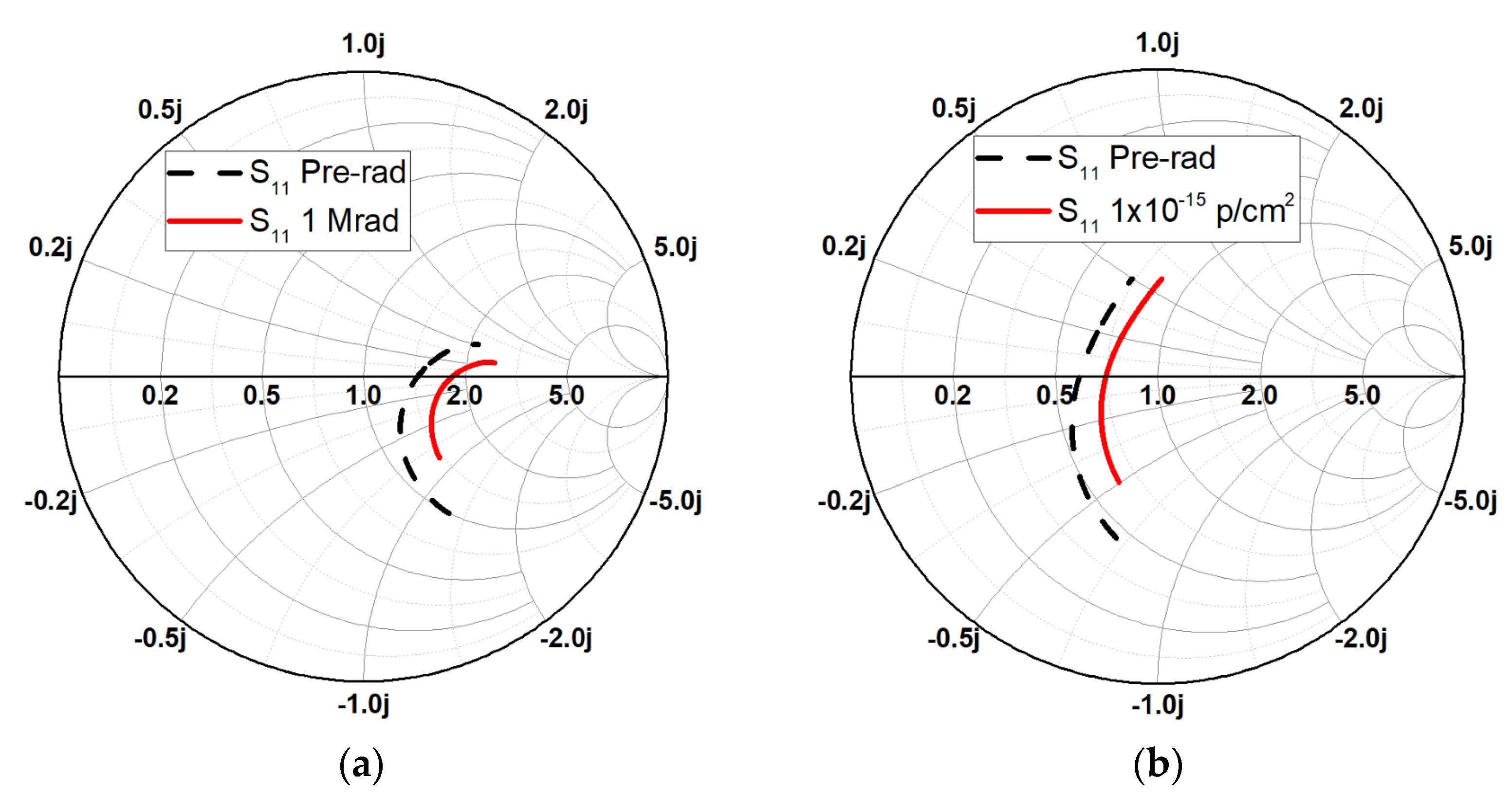
| Total Dose | S11 * | S22 * | S21 + | NF * |
|---|---|---|---|---|
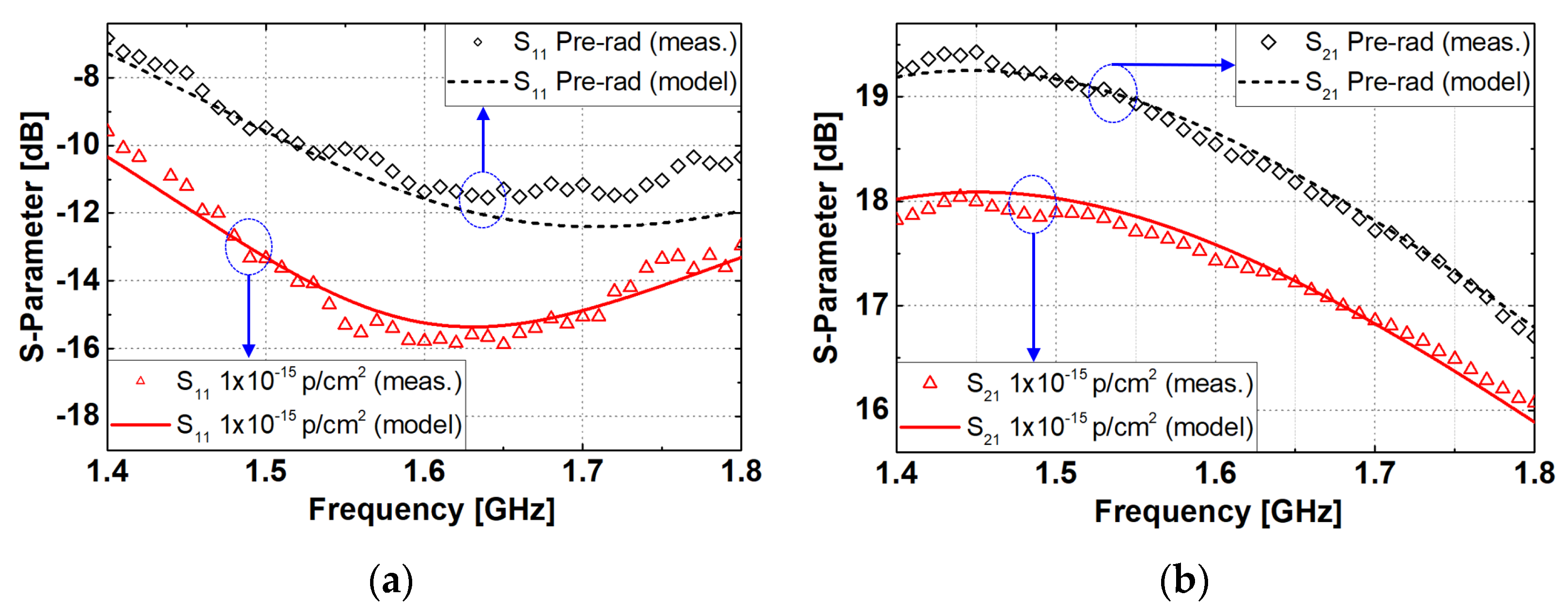
| Pre-irradiation | −15.62 dB | −23.66 dB | 12.89 dB | 3.45 dB |
| 500 krad | −11.52 dB | −17.11 dB | 7.34 dB | 5.6 dB |
| 1 Mrad | −11.27 dB | −11.19 dB | 7.14 dB | 5.66 dB |
| 3 Mrad | −11.79 dB | −17.36 dB | 7.55 dB | 5.78 dB |
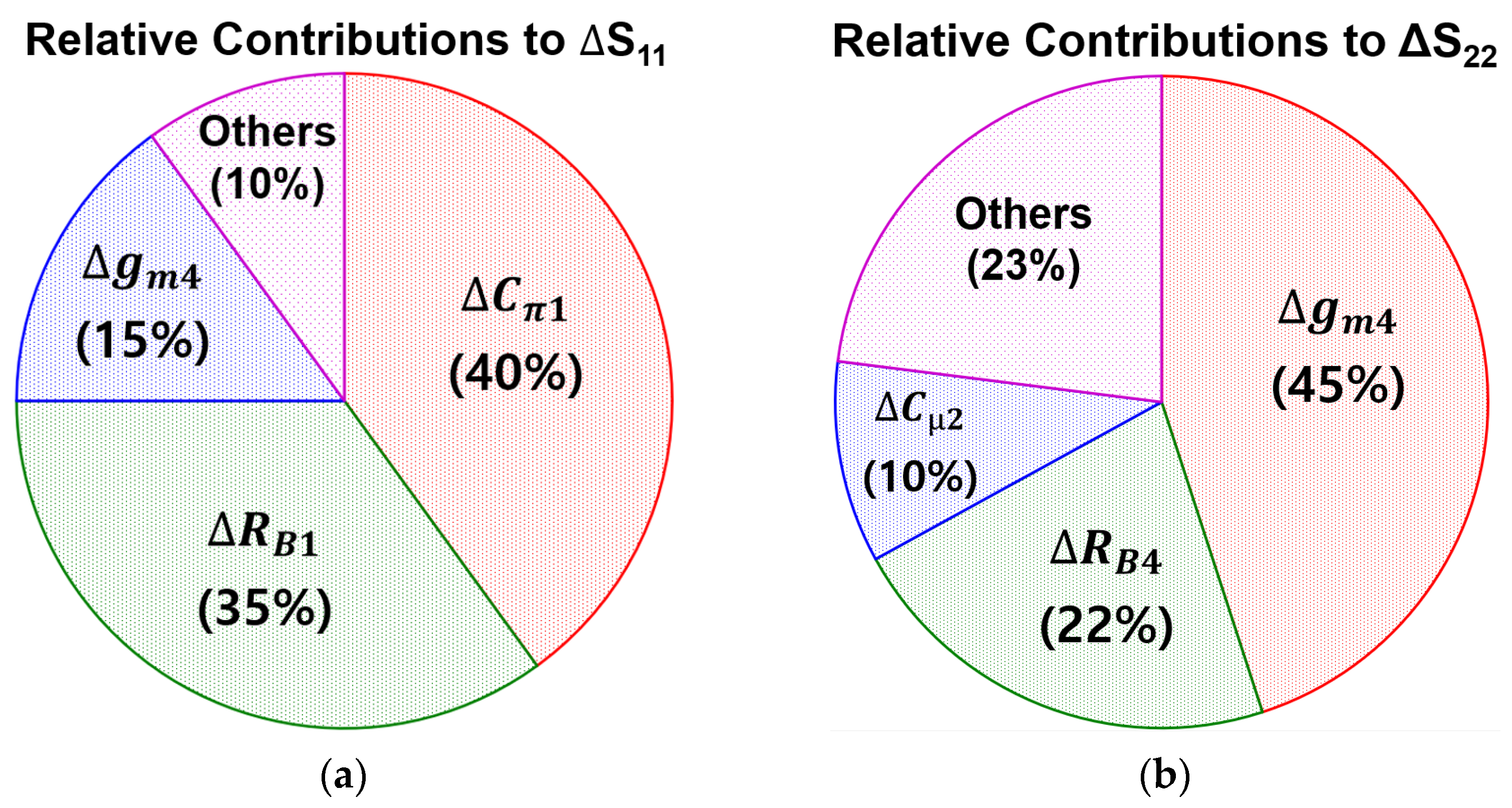
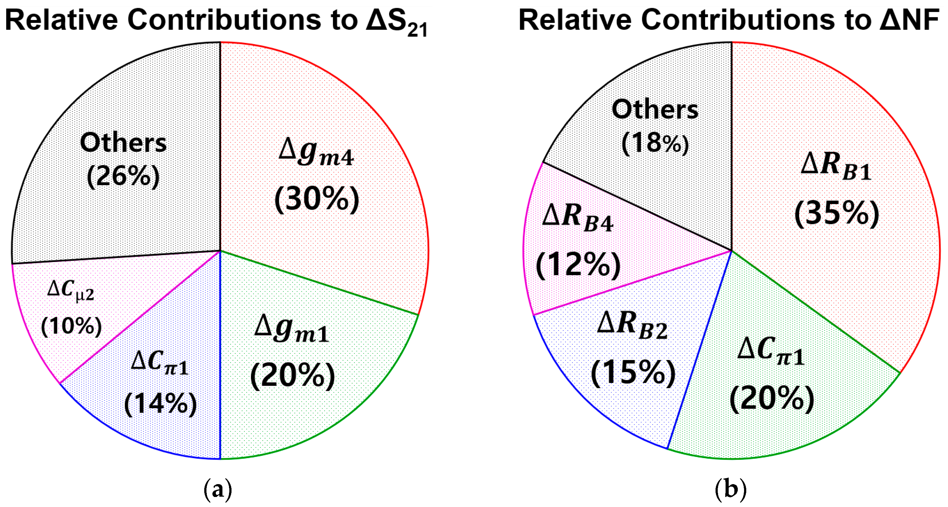
| Performance Metric | Contribution Rank #1 | Contribution Rank #2 | Contribution Rank #3 | Portion in the Total Degradation |
|---|---|---|---|---|
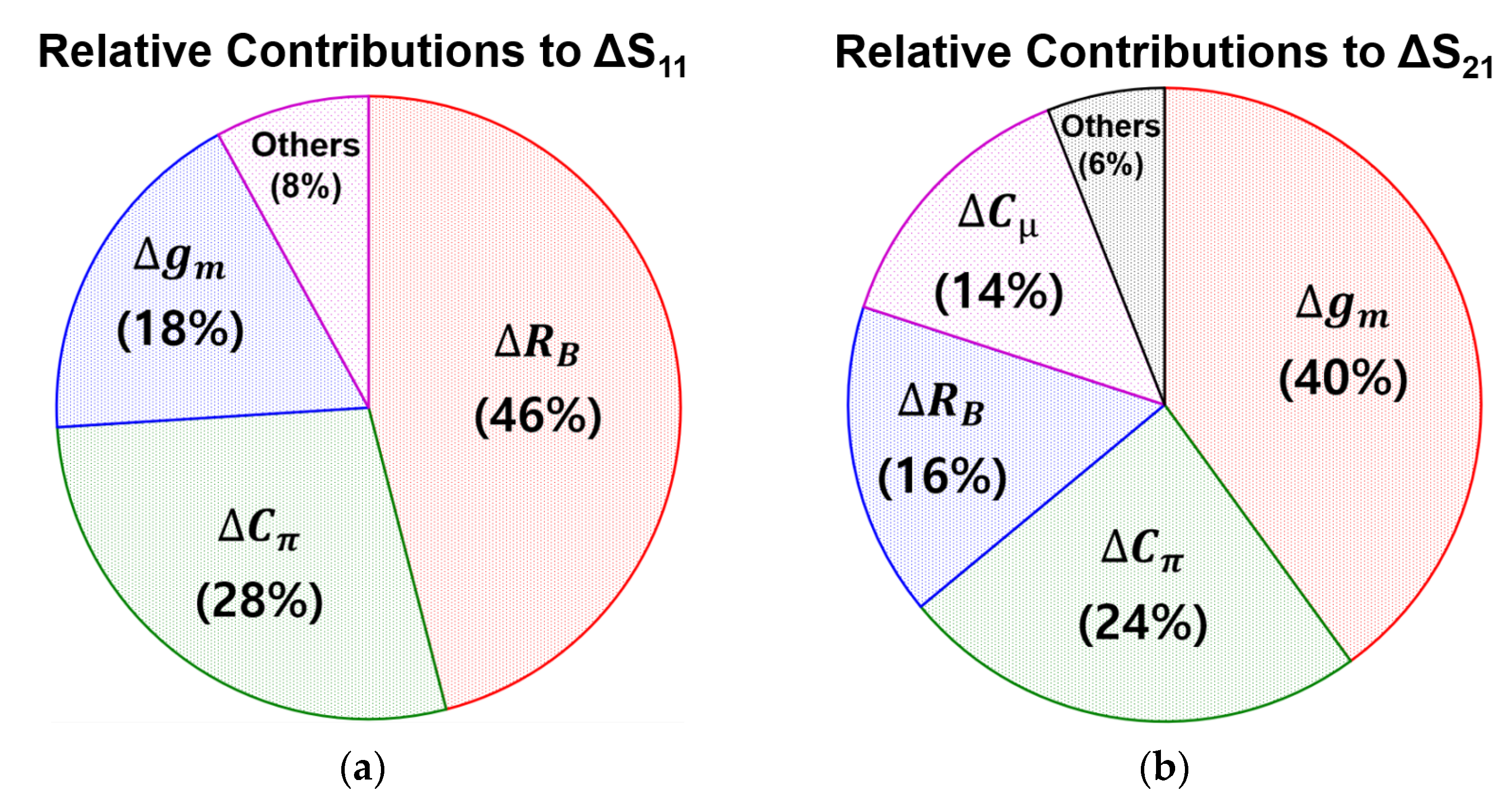
| ΔS11 | Cπ1 (40%) | RB1 (35%) | gm1 (15%) | 90% |
| ΔS22 | gm4 (45%) | RB4 (22%) | Cμ2 (10%) | 77% |
| ΔS21 | gm4 (30%) | gm1 (20%) | Cπ1 (14%) | 64% |
| ΔNF | RB1 (35%) | Cπ1 (20%) | RB2 (15%) | 70% |
| Parameter | Unit | Pre-Irradiation | Post-Irradiation (1 Mrad) |
|---|---|---|---|
| Cπ1, Cπ2 | fF | 250 | 475 |
| Cπ4 | fF | 240 | 430 |
| Cμ1, Cμ2 | fF | 15 | 28 |
| Cμ3, Cμ4 | fF | 13 | 25 |
| gm1, gm2 | mS | 45 | 38 |
| gm4 | mS | 17 | 13 |
| RB1, RB2 | Ω | 100 | 120 |
| RB4 | Ω | 90 | 110 |
Disclaimer/Publisher’s Note: The statements, opinions and data contained in all publications are solely those of the individual author(s) and contributor(s) and not of MDPI and/or the editor(s). MDPI and/or the editor(s) disclaim responsibility for any injury to people or property resulting from any ideas, methods, instructions or products referred to in the content. |
© 2024 by the authors. Licensee MDPI, Basel, Switzerland. This article is an open access article distributed under the terms and conditions of the Creative Commons Attribution (CC BY) license (https://creativecommons.org/licenses/by/4.0/).
Share and Cite
Kim, T.; Ryu, G.; Lee, J.; Cho, M.-K.; Fleetwood, D.M.; Cressler, J.D.; Song, I. Simple Modeling and Analysis of Total Ionizing Dose Effects on Radio-Frequency Low-Noise Amplifiers. Electronics 2024, 13, 1445. https://doi.org/10.3390/electronics13081445
Kim T, Ryu G, Lee J, Cho M-K, Fleetwood DM, Cressler JD, Song I. Simple Modeling and Analysis of Total Ionizing Dose Effects on Radio-Frequency Low-Noise Amplifiers. Electronics. 2024; 13(8):1445. https://doi.org/10.3390/electronics13081445
Chicago/Turabian StyleKim, Taeyeong, Gyungtae Ryu, Jongho Lee, Moon-Kyu Cho, Daniel M. Fleetwood, John. D. Cressler, and Ickhyun Song. 2024. "Simple Modeling and Analysis of Total Ionizing Dose Effects on Radio-Frequency Low-Noise Amplifiers" Electronics 13, no. 8: 1445. https://doi.org/10.3390/electronics13081445