Article

Improving Low-Frequency Digital Control in the Voltage Source Inverter for the UPS System

by
Zbigniew Rymarski
Department of Electronics, Electrical Engineering and Microelectronics, Faculty of Automatic Control, Electronics and Computer Science, Silesian University of Technology, Akademicka 16, 44-100 Gliwice, Poland
Electronics 2024, 13(8), 1469; https://doi.org/10.3390/electronics13081469
Submission received: 18 March 2024 / Revised: 4 April 2024 / Accepted: 10 April 2024 / Published: 12 April 2024

Abstract

:
Today voltage source inverters (VSIs) operate with high switching frequencies (let us assume higher than 50 kHz) owing to the fast Si (Silicon) or SiC (Silicon Carbide) switching transistors. However, there are some applications, e.g., with slower switches (e.g., IGBT—Isolated Gate Bipolar Transistor) or when lower dynamic power losses are required when the switching frequency is low (let us assume about 10 kHz). The resonant frequency of the output filter is usually below 1 kHz. The measurements of Bode plots of the measurement traces of various microprocessor-controlled VSIs show that in this frequency range, the characteristics of these channels can be simply approximated through two or three switching periods delay. For the high switching frequency, it is not noticeable, but for the low frequency it can cause some oscillations in the output voltage. One of the solutions can be to use the predictor of the measured state variables based on the full-state Luenberger observer or the linear Kalman filter. Both solutions will be simulated in MATLAB/Simulink and the chosen one will be tested in the experimental VSI. The research aims to omit delays in the measurement channels for the low switching frequency by using the predictions for the measured state variables and finally increasing the gains of the controller to decrease the output voltage distortions.

1. Introduction

The standard single-phase voltage source inverter (VSI) consists of the H-bridge (Si, SiC MOS-transistors, GaN hybrid transistors or IGBT transistors) and the output LC filter. The most important load for low-power voltage source inverters (<3 kW) is the nonlinear rectifier RC load according to the IEC 62040 standard [1] for UPS systems [1]. It defines that this load should have a power factor PF = 0.7 (calculated using Budeanu theory [2]). This load causes distortions of the output voltage that should be decreased by the control loop to the required total harmonic distortion (THD) level [1,3].
The approach to the control presented in this paper should be easily applicable in the microprocessor-controlled loops. There are many solutions for the control of the nonlinear plants (e.g., the inverter). The nonlinear control function can be approximated by a Fourier series [4] or the nonlinear inverter can be modelled using the Hammerstein approach [5]. However, modelling the inverter as a linear system for small increments around the operating point has been successfully practiced for many years [6] and is much easier in microprocessor implementation when the output voltage distortions are sufficiently low.
Every conventional control requires a model of the plant. The easiest continuous model is simply the transfer function of the output LC filter (1) and the transfer function of the PWM modulator, H(s) = exp(−sTs), a simple one switching-period delay (in the current switching-period delay we store the width of the next period pulse) for the resistive RLOAD. The equivalent series resistance (ESR) RC (Figure 1) of the filter MKP capacitor CF is neglected. The serial equivalent resistance RL is a sum of all of the serial resistances in the VSI including the result of the power loss in the core of the filter coil. More sophisticated is the quasi-continuous transfer function of the inverter (2), taking into account the Zero-Order-Hold method (in the discrete control) and the delay Ts of the PWM modulator [7].
K C T R L ( s ) = V O U T ( s ) V C T R L ( s ) e s T s 1 L F C F s 2 + ( R L L F + 1 R L O A D C F ) s + ( 1 + R L R L O A D ) 1 L F C F
K C T R L ( s ) = ( 1 s T s 2 ) 1 s T s 2 1 + s T s 2 1 L F C F s 2 + ( R L L F + 1 R L O A D C F ) s + ( 1 + R L R L O A D ) 1 L F C F
In both approaches of modelling, (1) and (2), the load resistance RLOAD is a model component. It means that the inverter model depends on the load. The solution is to measure the load current and treat it as an independent disturbance or the state variable [8,9,10,11,12,13]. The disadvantage of such a solution is losing the dependence between the output voltage and the output current. However, it is the most commonly used approach to inverter modelling.
Today the control is only digital, using microprocessors or FPGA. We need a discrete model [14,15,16,17] of the inverter where the output voltage, the inductor current and the output current are state variables and the output voltage is an output variable of the inverter model.
The design of the output LC filter depends on the demands of damping the output ripple voltage in the steady state and decreasing overvoltage during dynamic load changes (mainly step decreasing the load).
The control loop can be a single-input single-output (SISO) type when only the output voltage is measured and controlled or a multi-input single-output (MISO) when the measured output voltage, output current and the output filter inductor current are inputs of the controller and the output voltage is controlled [16,17]. MISO control is more effective [15] because in SISO control, the output current is the unmeasured disturbance. One of the MISO control systems that seems to be predicted for power systems is passivity-based control [18,19,20,21,22,23,24,25]. This is based on the idea that the stable system should be passive (energy stored is less than energy supplied). The idea of this control is to “inject” appropriate damping (resistance) to get the passivity of the system. The energy of the system is presented as the Hamiltonian function.
The last problem is the transfer function of the measurement and control traces. The PWM modulator has one switching-period delay. The currents and voltage measurement traces are a kind of low-pass filter. The output filter transfer function usually has a resonant frequency below 1 kHz. As a result, the transfer function of the measurement traces is important below this frequency. All three measurement traces are the same except for the first isolation stage. Current traces have LEM transducers, and the voltage trace has an isolation amplifier. It is possible to assume that all three traces have the same transfer function in the frequency range up to 1 kHz. It will be shown that in this frequency range, this transfer function can be modelled by the two or three switching periods delay, which means that the transfer function depends more on the digital sampling and data conversion than on the analogue properties of the trace.
We consider two switching frequencies: 12,800 Hz assumed as the low switching frequency and 51,200 Hz as the high switching frequency. For the high switching frequency, the delay is so low that it does not matter in control [17]. For the low switching frequency, the control can cause an oscillation component in the output sinusoidal voltage. Sometimes the preferable operation is the one with a low switching frequency that requires higher LC filter values but has lower switching losses (particularly for IGBT transistors in H-bridge).
There are many solutions for control in systems with delay [26,27,28,29,30]. One of the most common solutions is the Smith Predictor [28]. However, we want to solve the problem in a simplified way—to design an MISO PBC controller for the system without delay in the measurement traces and implement it in the system with delays using the prediction of the measured state variables. This approach was shown in [17] where the simplified Luenberger observer was used for prediction. Only output voltage was used as the output variable in this prediction. The result of the control with this prediction was promising [17]. However, in this paper the Luenberger observer with all the three measured variables treated as outputs in the prediction will be used, giving lower distortions of the output voltage. For comparison, the Kalman filter was used for the prediction, but its implementation in the standard microprocessor can be troublesome. The simulation of the system with the Kalman filter as a predictor will be shown to compare it with the Luenberger observer.
Section 2 presents the design of VSI, Section 3 presents the discrete model of VSI, Section 4 presents the Bode plots of the measuring traces (channels), Section 5 presents the design of the MISO PBC controller, Section 6 presents the design of the predictor with the full-state Luenberger observer, Section 7 presents the simulation of the low switching frequency VSI control with the linear Kalman filter, Section 8 presents the comparison of the results of the simulations and the choice of the predictor, Section 9 presents the experimental verification of the simulations, Section 10 presents the description of the general results of the simulations and breadboard verification, Section 11 presents discussion on the advantages of predictor usage and Section 12 presents a short conclusion.

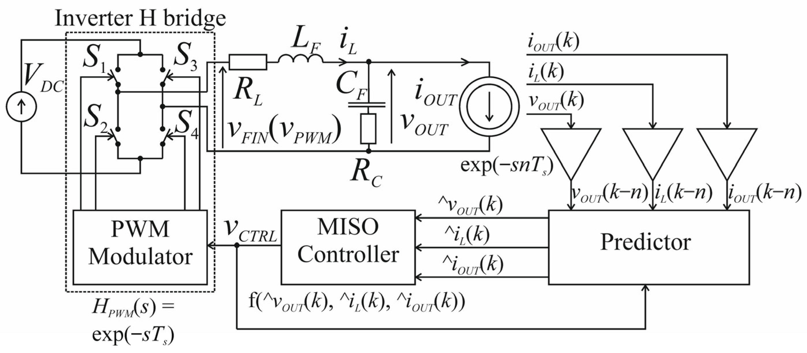
2. Design of the VSI
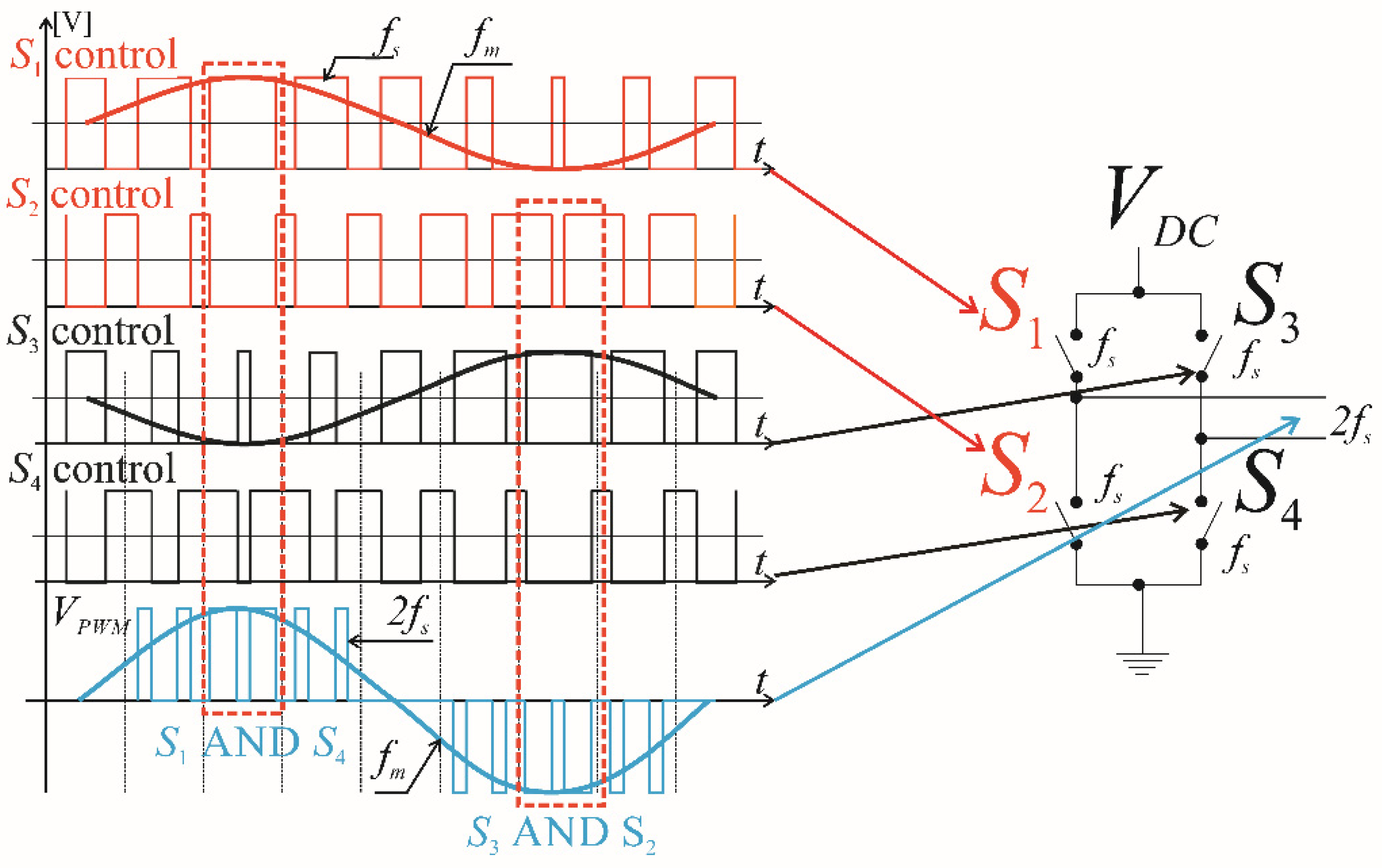
2.1. PWM Scheme

Figure 2 presents the idea of the so-called 1-scheme of 3-level modulation [31]. The upper H-bridge transistors of both bridge legs (S1 and S3) are driven with the pulse series shifted with half of the fundamental period. Both waveforms are sinusoidal summed with a constant value equal to half of their amplitude. The characteristic feature of this PWM scheme is the double switching frequency 2fs in the output.

2.2. The Output Filter Design

The fundamental problem of VSI design is to calculate the values of the output filter inductor and capacitor (the whole model of VSI depends on them). Fundamental frequency fm = 50 Hz. The idea presented in [32] and further in [14] was to calculate the LFCF product to restrict output voltage ripple (an approximately parabolic waveform that has switching frequency fs equal to fs or 2 fs depending on the modulation scheme) amplitude hnmax (fs) to 3% of the fundamental amplitude (IEEE-519 [3]). Then the cost function, which is the sum of modules of reactive powers in the inductor and capacitor, is created. It was shown that the output impedance of the VSI depends mainly on the inductance of the filter coil in the low-frequency range (below the resonant frequency of the output filter). Some authors [33,34] multiply the module of the reactive power in the inductor by the coefficient over unity. In the presented Equations (3) and (4) there were no coefficients. These dependencies are calculated for the 3-level PWM modulation [14].
L F 1 f s V O U T r m s I O U T r m s = 1 f s R O U T n o m
C F 1 f s 1 V O U T r m s / I O U T r m s = 1 f s 1 R O U T n o m
Let us assume fs = 12,800 Hz, and that for the 1-scheme of modulation the output filters operate at fs’ = 2fs = 25,600 Hz. For RLOAD = 50 Ω, the calculated values of LF = 2 mH, CF = 0.8 μF and LFCF = 1.6 × 10⁻⁹ s2 are suitable for the static load.
The feedback does not respond during one switching period Ts (the pulse width data are calculated and stored in one switching period and set the pulse width in the next switching period) and we can treat the filter inductor LF as the current source in one switching period. For the step load current decrease, e.g., ΔiOUT = −5 A, the overvoltage pulse will be TsΔiOUT/CF = 500 V. When the value of the CF capacitor was increased to 50 μF, the overvoltage was 7.8 V. The value of LF can be decreased to 1 mH. The resonant frequency of the filter is 712 Hz. The capacitor is an MKP type with a low ESR [35,36]. The coil LF requires a low power loss core. Ferrites (MnZn or NiZn) have low saturation flux density. It seems that the best choice would be an alloy-powder material [37,38] with low power losses [39], allowing the almost constant inductance value of the filter coil in the wide switching frequency range.

2.3. The H-Bridge

The H-bridge has MOSFET IRFP360LC switches driven by IR2184 circuits. The serial drain-source on-state resistance is 0.2 Ω. An STM32V407VG microprocessor controls the VSI. The highest frequency fCOMP on the input of the comparator in the PWM unit is 84 MHz. For fs = 12,800 Hz, we can set fCOMP/fs = 6562 signal levels. This means that the resolution of the generated sinusoidal signal (amplitude of the reference waveform is 3281), equal to 0.000305, is almost equal to the smallest change 0.000301 of the exact sinusoidal waveform during one switching period, close to π/2 or 3π/2 (the worst case). In the case of fs = 25,600 Hz, we can set fCOMP/fs = 3281 signal levels (1640 per amplitude). This means that the resolution of the generated signal, equal to 0.00061, causes the clustering of some of 512 pulses per fundamental period. However, this kind of error for fCOMP = 84 MHz is negligible.
The DC serial resistance of the filter coil (with Super-MSS core [37]) is 0.2 Ω but the power losses [39] cause its increase for the AC magnetising current (with fs switching frequency) [38]. A serial equivalent resistance for the used switching frequencies was assumed, for the load current range RL = 1 Ω. The used drivers introduced 0.5 μs of dead time Tdt. Dead time decreases the PWM pulse width by the constant value. It makes the short pulses vanish. For the 3-level PWM, the absolute value of the output voltage is decreased when the output current changes its sign. This effect increases the output voltage distortion (total harmonic distortion THD) proportionally to the switching frequency for the simulated PWM voltage. THD is calculated to the 15 harmonics (750 Hz) because it will be the resonant frequency of the output LC filter. It is presented in Figure 3 for the modulation index M = 0.8, neglecting the output filter impact. With Tdt = 0.5 μs, for fs = 12,800 Hz, ΔTHD = 0.46%; for fs = 25,600 Hz, ΔTHD = 0.93%; and for fs = 51,200 Hz, ΔTHD = 1.90%. There are some solutions to decrease the influence of dead time, e.g., properly shaping the reference voltage but this is not a subject of this paper. The higher the switching frequency, the higher the additional distortions.

3. The Discrete Model of VSI

The continuous description of the VSI using state equations is simple. For the state-space variables x = [vOUT iLF iOUT]T, input variable u = vFIN (Figure 1) and output variable y = vOUT, the state equations (for RC = 0) are (5) and (6).
x ˙ = A x + B u ,   y = C x
where
A = 0 1 C F 1 C F 1 L F R L L F 0 0 0 0 ,   B = 0 1 L F 0 , C = 1 0 0
The state-space equations can be solved in the switching period [6]. The solution is the exponential function of TON time, which depends on the PWM modulation type. For 3-level, double-edge modulation the exponential matrix can be approximated
e A T O N k / 2 = I + A T O N k / 2 + A 2 T O N k 2 / 4 I + A T O N k / 2
The final linearized discrete state-space equations [14] are (8) where vCTRL is the input of the PWM modulator.
x ( k + 1 ) = A D x ( k ) + G D T O N ( k ) = A D x ( k ) + G D T s V D C v C T R L ( k )
y ( k + 1 ) = C D x ( k )
where the matrixes are (9).
A D = Φ ( T s ) = ϕ 11 ϕ 12 ϕ 13 ϕ 21 ϕ 22 ϕ 23 ϕ 31 ϕ 32 ϕ 33 , G D = g 11 g 21 g 31 , C D = C
ω F 0 = 1 C F L F ,   ξ F = 1 2 R L F e C F L F ,   E φ = exp ( ξ F ω F 0 T s ) ,   E g = exp ( ξ F ω F 0 T s / 2 ) ,
ϕ 11 = [ cos ω F 0 T s + ξ F sin ω F 0 T s ] E φ ,   ϕ 12 = 1 ω F 0 C F sin ( ω F 0 T s ) E φ ,   φ 13 = φ 12 + R L ( φ 11 1 )
ϕ 21 = C F L F φ 12 ,   ϕ 22 = [ cos ( ω F 0 T s ) ξ F sin ( ω F 0 T s ) ] E φ ,   ϕ 23 = 1 φ 11 ,
ϕ 31 = 0 ,   ϕ 32 = 0 ,   ϕ 33 = 1 ,
g 11 = V D C ω F 0 sin ( ω F 0 T s / 2 ) E g ,   g 21 = V D C L F [ cos ( ω F 0 T s / 2 ) ξ F sin ( ω F 0 T s / 2 ) ] E g ,   g 31 = 0 .
The presented (8) discrete state-space equations enable the design of the controller and predictor presented in Figure 1.

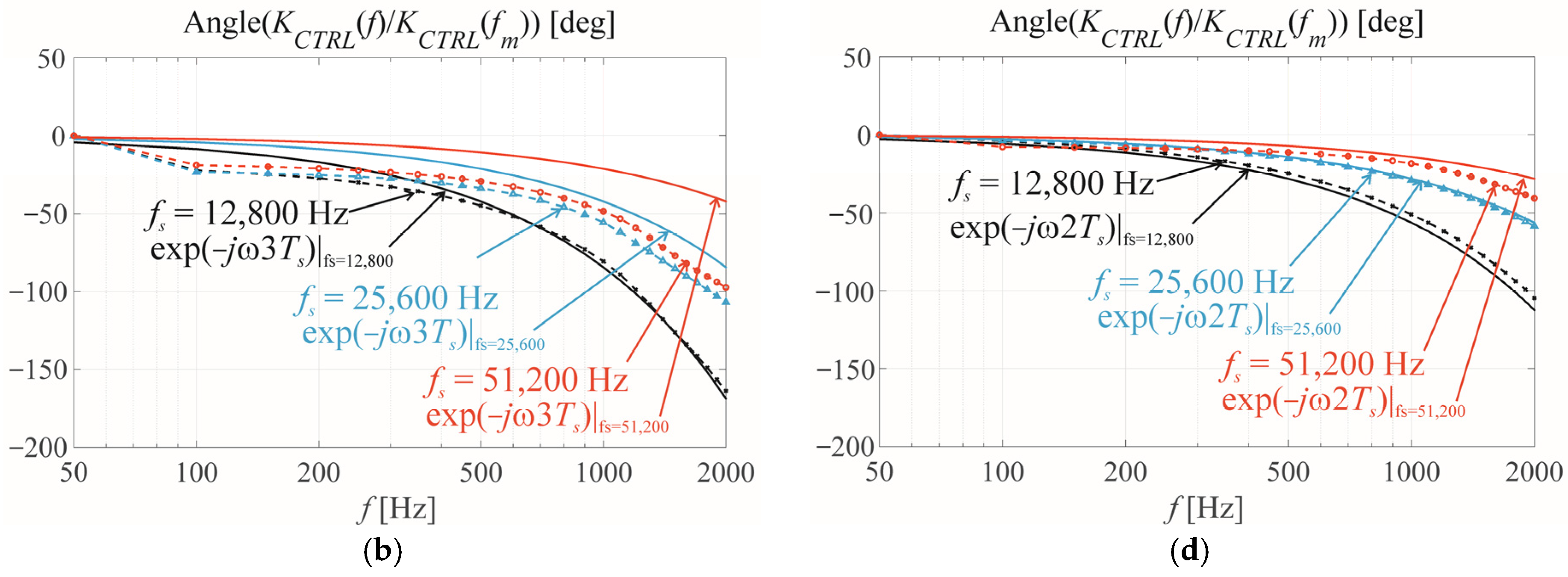
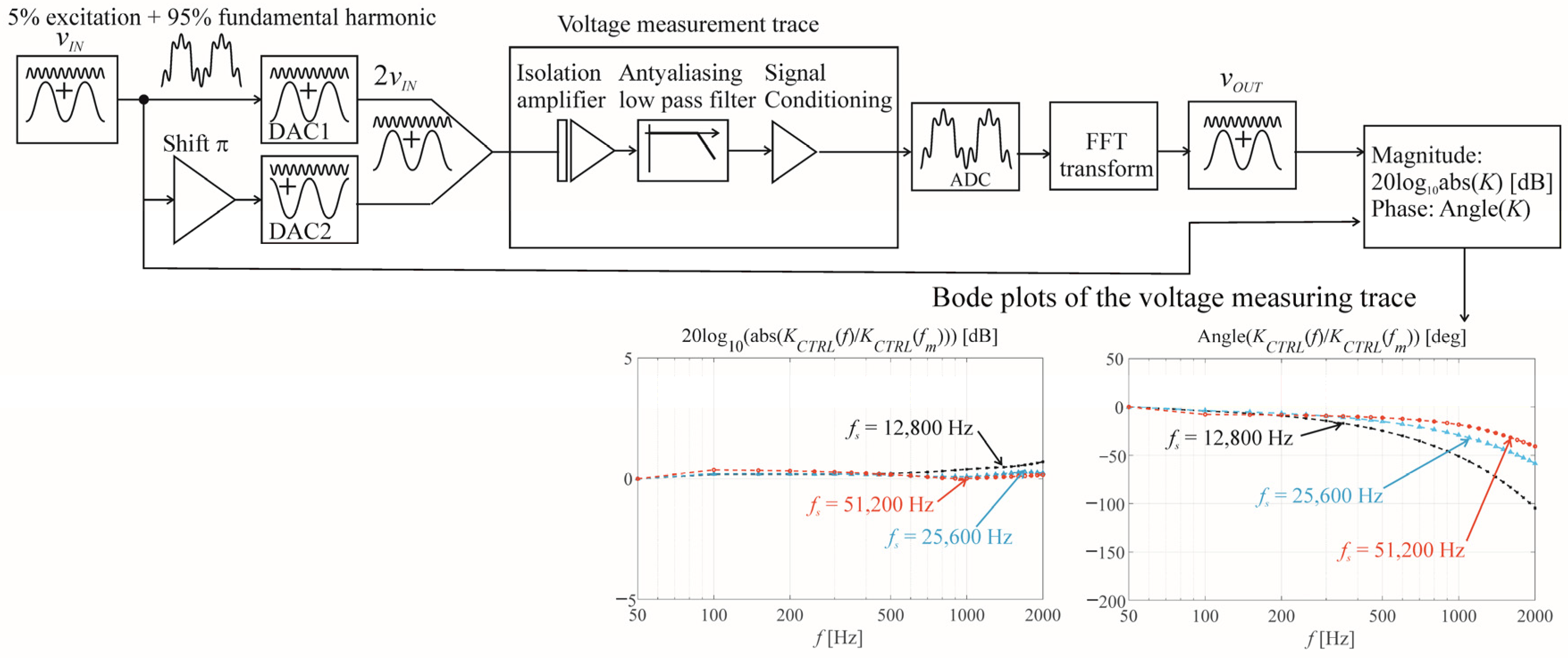
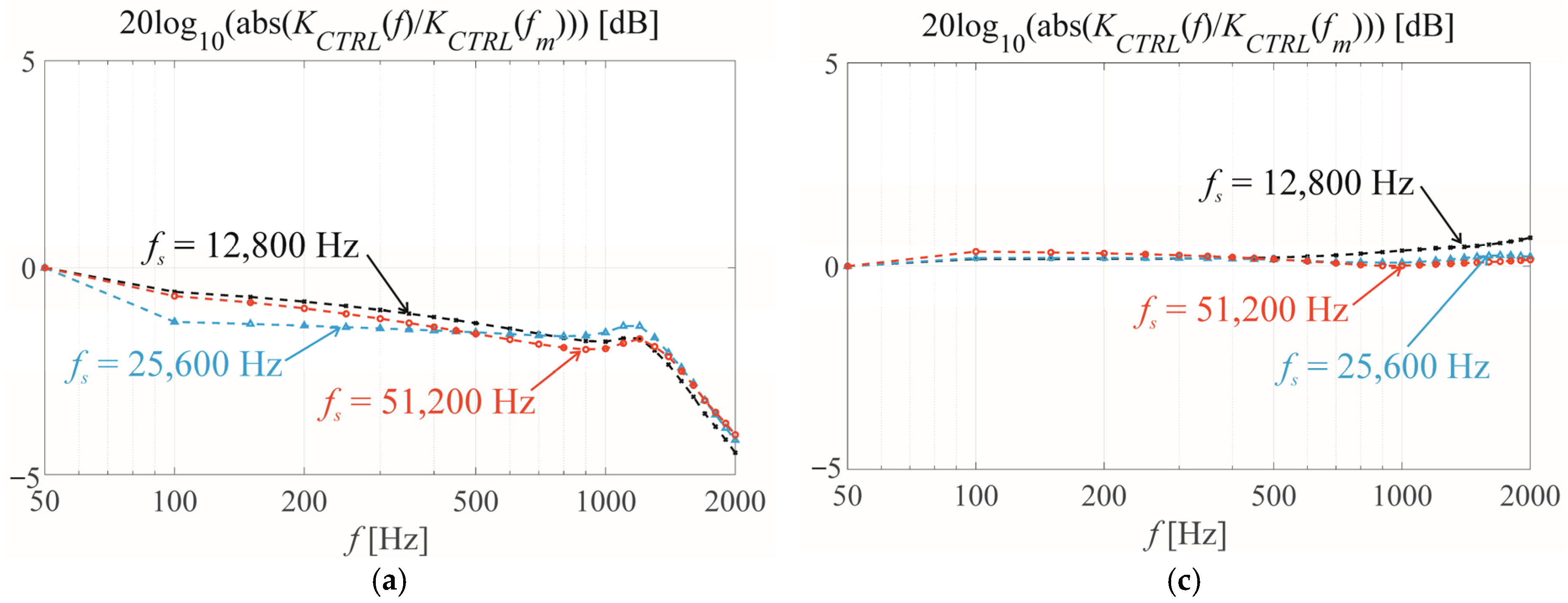
4. Bode Plots of the Measuring Traces

There are two current and one voltage measuring traces. All of them have similar designs except the input. The fast transducers are in the current traces and the isolation amplifier is in the voltage trace. In the measured frequency range of 50–5000 Hz, their frequency-dependent characteristics do not notably make a difference in the whole-trace Bode plots. As a result, Bode plots of one voltage measuring channel will be shown. The idea of measuring Bode plots of the voltage channel in the VSI is shown in Figure 4. In the experimental VSI, the PWM signal and this signal shifted with half of the fundamental period are driving two digital-to-analogue converters (internal DAC1 and DAC2 from STM32F407VG), and the difference between their outputs was connected to the input of the voltage measuring trace. The output signal of the trace was measured. There are different units for the input signal, volts, and the output measured using analogue-to-digital converter ADC, units of the 13-bit converter (12-bits and the sign, −4095 to 4095). As a result, it is not possible to compare the output signal in units and the input signal in volts. The solution presented in [40] for measuring the real parameters of VSI is the “relative” way of measuring. The quotient of the ratios of excitation and the fundamental waveform in the output and input were measured (Figure 4). The assumption was that the fundamental waveform was not suppressed or shifted. However, in this way, it is not possible to measure the “proportional gain” (Figure 5). In the real VSI, this gain was adjusted to get the amplitude of the measured signal to about ¾ of the full scale of the ADC for the nominal load. Adjusting the channel gain is called scaling and is described in [41].
For k = 1 to fs/fm, the amplitude of the fundamental harmonic A was set to 0.95 and the amplitude of kfm excitation was 1 − A (10).
V C T R L ( k ) = r o u n d ( M · f l o o r 1 2 f C O M P f s ( A sin ( k 2 π f s / f m ) + ( 1 A ) sin ( n k 2 π f s / f m ) ) )
The magnitude Bode plot is as in (11).
K I N V ( n f n ) = 20 log V O U T ( n f m ) / V O U T ( f m ) V C T R L ( n f n ) / V C T R L ( f m )
The phase Bode plot is as in (12).
arg ( n f m ) = [ arg ( V O U T ( n f m ) ) arg ( V O U T ( f m ) ) ] [ arg ( V C T R L ( n f m ) ) arg ( V C T R L ( f m ) ) ]
Finally, it was shown in Figure 5 that for the low and middle switching frequencies (fs = 12,800 Hz and fs = 25,600 Hz), the Bode plots in the frequency range below 1000 Hz can be approximated by the simple delay exp(−jωnTs), where n = 2 or 3. This demonstrates that the Bode plots in this frequency range depend much more on the digital signal processing in the microprocessor than on the analogue properties of the measuring channel.

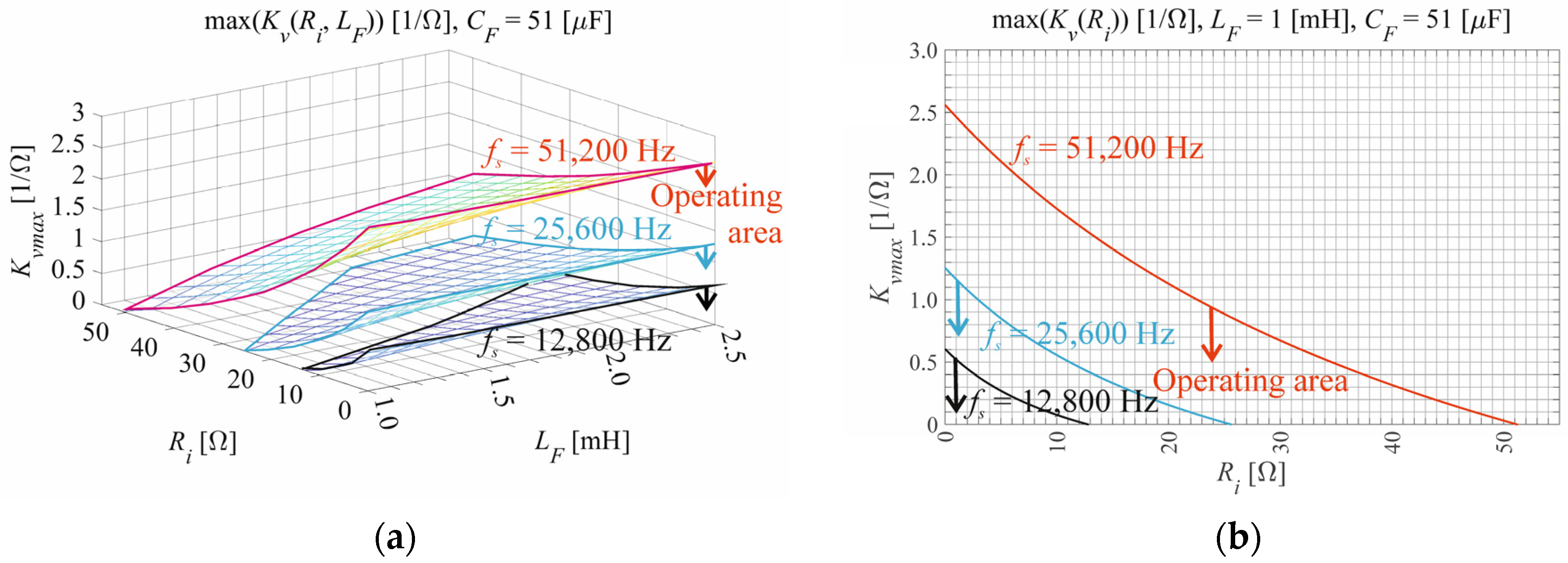
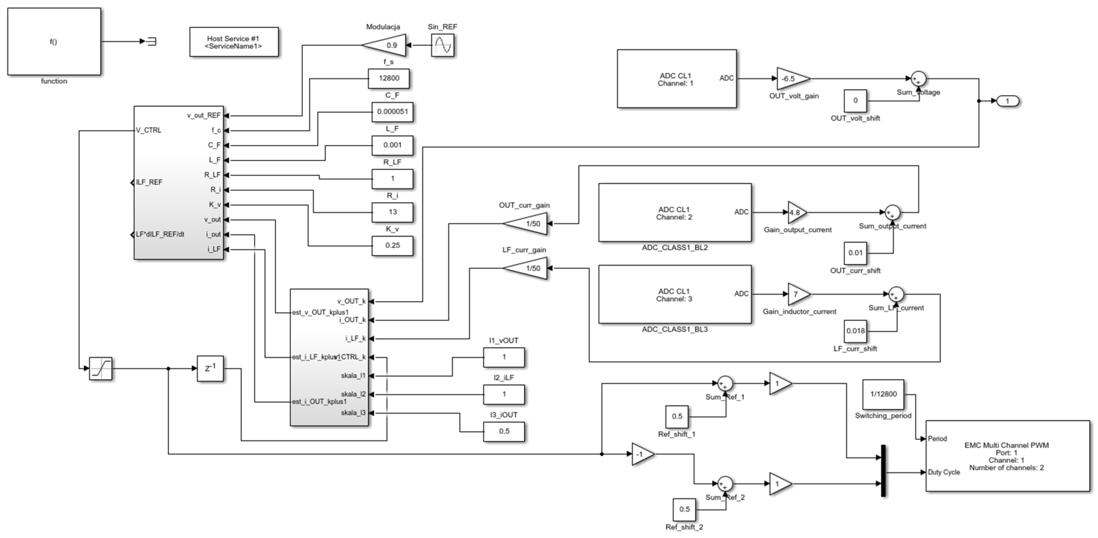
5. The MISO PBC Controller

The passivity-based control [18,19,20,21,22,23,24,25] considers the energy stored in the system (considering Hamiltonian function (13), similar to the Lyapunov function [23]) that should be lower than the energy delivered to the system. The basic solution was only “injecting” the additional “resistance” (treated as the current error gain) into the system. The output voltage was relatively controlled. The newer solution [23,24] was the direct implementation of the output voltage error gain to the control system.
H ( x ) = 1 2 ( L F i L F 2 + C F v O U T 2 )
The discrete control laws of PBC [16,17] according to Figure 1 where we consider the predicted state variables  x ^ , are (14) and (15).
v ^ C T R L ( k ) = R i i ^ L F ( k ) + ( R i + R L F ) i ^ L F r e f ( k ) + L F i ^ L F r e f ( k ) i ^ L F r e f ( k 1 ) T c + v O U T r e f ( k )
i ^ L F r e f ( k ) = K v [ v O U T r e f ( k ) v ^ O U T ( k ) ] + C F v O U T r e f ( k ) v O U T r e f ( k 1 ) T c + i ^ O U T ( k )
In the control law, there are two gains—basic current gain Ri (“injected” damping) and the additional voltage gain Kv. It was shown for the continuous version of PBC that for RL + Ri > 0 and Kv > 0, the roots of the characteristic equation of the closed loop system with PBC are always in the left half-plane s and the system is stable. For positive values of gains, this condition is always met. However, the discrete 3-level modulation PWM modulator has a limit for the output voltage increase in speed of VDC/Ts. The increase in the control voltage from (14) cannot be faster than the modulator possibility [16,17,41]. This means that Equation (16) should be filled.
d v C T R L ( k T s ) d t V D C T s
The restriction [16,17,41] calculated from (14) and (15) for the worst case of the inverter load RLOAD = ∞ is (17).
K v [ L F + ( R i + R L ) T s ] 1 L F C F + R i L F < f s
It is obvious from (17) that the product RiKv is restricted and its tolerable maximum value is proportional to the switching frequency. The convergence of error is faster for the higher values of error gains. However, the higher values of the gains cause the saturation of the PWM modulator and can cause oscillations. The conclusion is that the PBC control results in lower distortions of the output voltage for the standard loads for the higher switching frequency. Figure 6 presents the results of Equation (17)—the possible operating areas of PBC as a function of gains Ri and Kv. However, a serious approximation was made when creating (17) and we can treat its result as the initial adjustment to make fine adjustments in the experimental model.

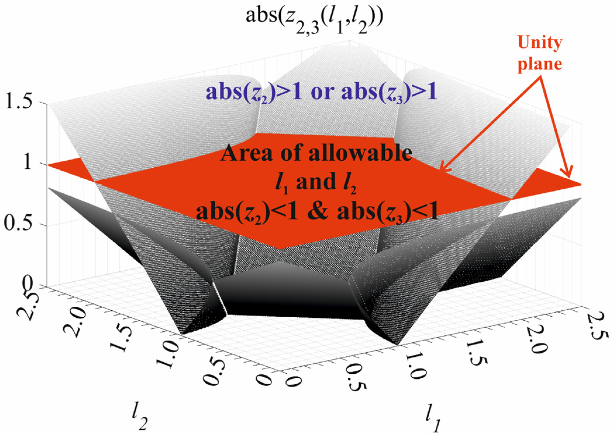
6. Predictor with the Luenberger Observer

The predictor should predict the state variables of the model in future switching periods using the state-space equations with the correction component. The full-order state Luenberger observer [42,43,44,45,46,47,48] or linear Kalman filter (MATLAB/Simulink) will be used. It will be shown in the simulation and experimental verification that prediction is important for the low switching frequency (it was assumed fs = 12,800 Hz) and is useless for the high switching frequency (it was assumed fs = 51,200 Hz) when a delay is low.
The state equations are described in (5)–(9). The difference of the current study from [17] is that 3 measured outputs (18) are assumed (previously only one: vOUT).
y = x, CD = eye(3)
The predicted state variables using the Luenberger observer are described in (19).
x ^ ( k + 1 ) = A D x ^ ( k ) + G D T O N ( k ) + L [ y ( k ) C D x ^ ( k ) ]
The error system is described by Equation (20).
e ( k + 1 ) = ( A D L C D ) [ x ( k ) x ^ ( k ) ] = ( A D L C D ) e ( k )
where for 3 measured outputs and 3 state variables the matrix of Luenberger gains is (21).
L = l 1 0 0 0 l 2 0 0 0 l 3
The characteristic equation of the full-state Luenberger observer is (22).
det ( z e y e ( 3 ) A D + L C D ) = 0
The roots of the characteristic equation of the observer (22) are independent of the closed-feedback-loop control system. This is the “separation theorem” [45]. The observer eigenvalues should enable a faster convergence to zero of the observation error than that of other transient processes in a closed-loop system. Better observer dynamics are obtained if the roots of their characteristic Equation (22 are closer to zero on the z-plane (their absolute value is lower) than the roots of the characteristic equation without estimation  det ( z 1 A D ) = 0 . Different examples demonstrate this assumption. The observer poles are selected to be closer to the origin than the open-loop poles at the same phase angle. In [45], the Luenberger observer was designed with its dynamics three times faster than the fastest pole of the plant. In [46,47,48] there is a similar approach in that the choice of observer gains should be a compromise between the bandwidth and noise elimination while the dynamics of the observer should be much faster than the open loop dynamics of the system.
The characteristic Equation (22) of the full-state Luenberger observer is shown in (23) and (24).
det z φ 11 + l 1 φ 12 φ 13 φ 21 z φ 22 + l 2 φ 23 0 0 z 1 + l 3 = 0
( z 1 + l 3 ) [ ( z φ 11 + l 1 ) ( z φ 22 + l 2 ) φ 12 φ 21 ]
The aim is to find the l1, l2 and l3 gains for which the system (20) is stable and possibly fast. There are 3 roots of characteristic Equation (24). All roots zi should be inside the unity circle in the z-plane (25).
z i < 1
The first root is z1 (26).
z 1 = 1 l 3
The second z2 and the third z3 roots will be calculated from (27).
z 2 + z ( l 1 + l 2 φ 11 φ 22 ) + ( l 1 l 2 φ 22 l 1 φ 11 l 2 + φ 11 φ 22 φ 12 φ 21 ) = 0
The roots z2 and z3 are described by Equation (28).
z 2 , 3 = [ ± [ ( l 1 l 2 ) + ( φ 22 φ 11 ) ] 2 + 4 φ 12 φ 21 ( l 1 + l 2 φ 11 φ 22 ) ] / 2
Figure 7 presents the area in which (25) is filled for z2 and z3 using (28) for fs =12,800 Hz, LF = 1 mH and CF = 51 μF.
The presented analysis shows that it can initially be assumed that l1 = 1, l2 = 1 and l3 = 0.5. Figure 8 presents the MATLAB/Simulink model of the low switching frequency VSI with prediction with Luenberger observer realising Equation (19).

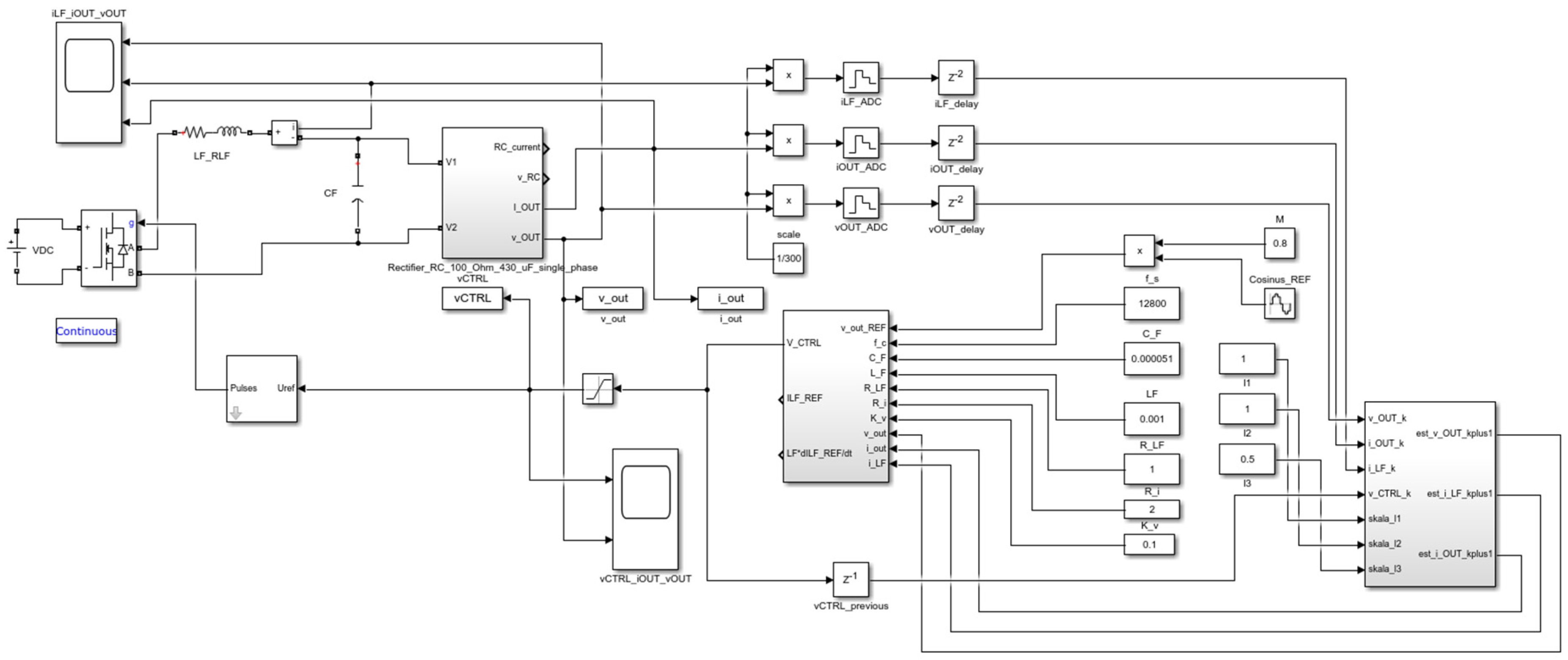
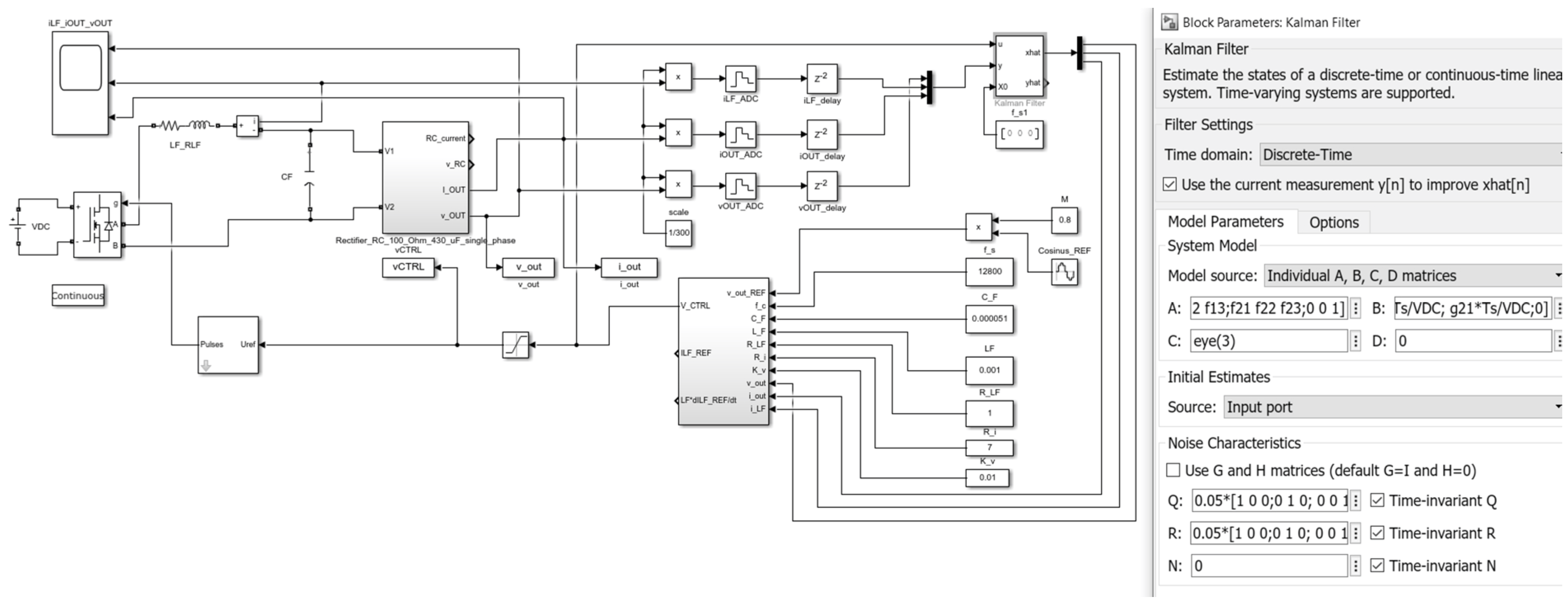
7. Simulation of the Low Switching Frequency VSI Control with the Linear Kalman Filter

The Kalman recursive filter [45,49,50,51,52,53,54] in its basic linear version can be used for the prediction of the state variables. In the state equation vk represents discretized process noise (29).
x k + 1 = A D x k + G D u k + v k
The measurement model with measurement noise is (30). Hk is the measurement matrix and wk is the measurement noise at the current k time step (30).
z k = H x k + w k
The prediction process is the first stage of the recursive algorithm of filtering. At the beginning of the filtering process, there is the state, x0/0, and the assumed state covariance, P0/0. The Kalman filter proceeds to the next steps in the closed loop. It will begin the “a priori” estimate (31) where the k + 1 step is propagated from the previous step k, which is notated as subscription k + 1/k.
x k + 1 / k = A D x k / k + G D T O N k
The covariance matrix P is propagated in a similar way (Q—process noise covariance matrix) (32).
P k + 1 / k = A D P k / k A D T + Q
The measurement vector is predicted for the next k + 1 period (33).
z k + 1 / k ( k ) = H x k + 1 / k
The correction process proceeds in a closed loop of filtering to correct the predicted values of state variables. The measurement prediction covariance is now computed (R—measurement noise covariance matrix) (34).
S k + 1 = H P k + 1 / k H T + R
The Kalman gain is computed (35).
K k + 1 = P k + 1 / k H T S k + 1 1
The difference between the actual measurement zk+1 and the predicted measurement zk+1/k is used to correct the state variables in the next period. The estimation after correction uses the subscript notation, k + 1|k + 1. The corrected state is called the “a posteriori” estimate.
x k + 1 / k + 1 = x k + 1 / k + K k + 1 ( z k + 1 z k + 1 / k )
The state covariance matrix is now corrected:
P k + 1 / k + 1 = P k + 1 / k K k + 1 S k + 1 K k + 1 T
Comparing the computed measurement based on the corrected state and the actual measurement it is possible to estimate the performance of the filter. Now the processes of prediction/correction are repeated. The initial conditions can be x0/0 = [0 0 0] and P0/0 = p*eye(3) (p is adjusted). The selection of coefficient values of covariance matrices Q and R of the Kalman filter is problematic [52]. A Simulink Kalman filter block was used with Q and R matrices equal to 0.05*eye(3) (Figure 9).
The basic steps of the computational procedure for the discrete-time Kalman estimator were as follows:
  • Compute Pk+1/k using Pk/k, ADk and Qk (32).
  • Compute Kk+1 using Pk+1/k (computed in step 1), Hk+1, and Rk+1 (34) and (35).
  • Compute Pk+1/k+1 using Kk+1 (computed in step 2) and Pk+1/k (from step 1), (37).
  • Compute successive values of xk+1/k+1 recursively using (36) the computed values of Kk+1 (from step 3), the given initial estimate x0 and the input data zk+1.

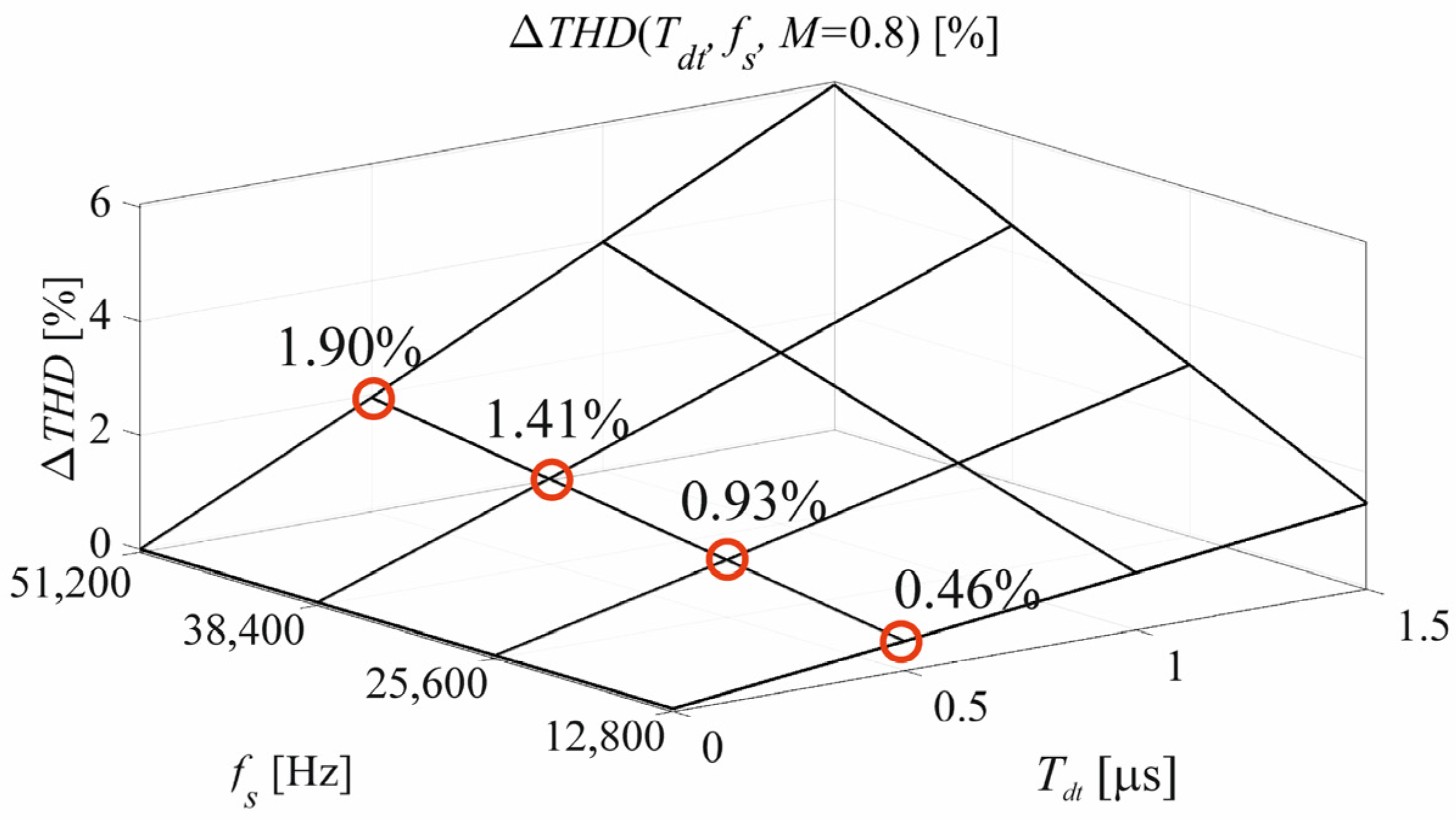
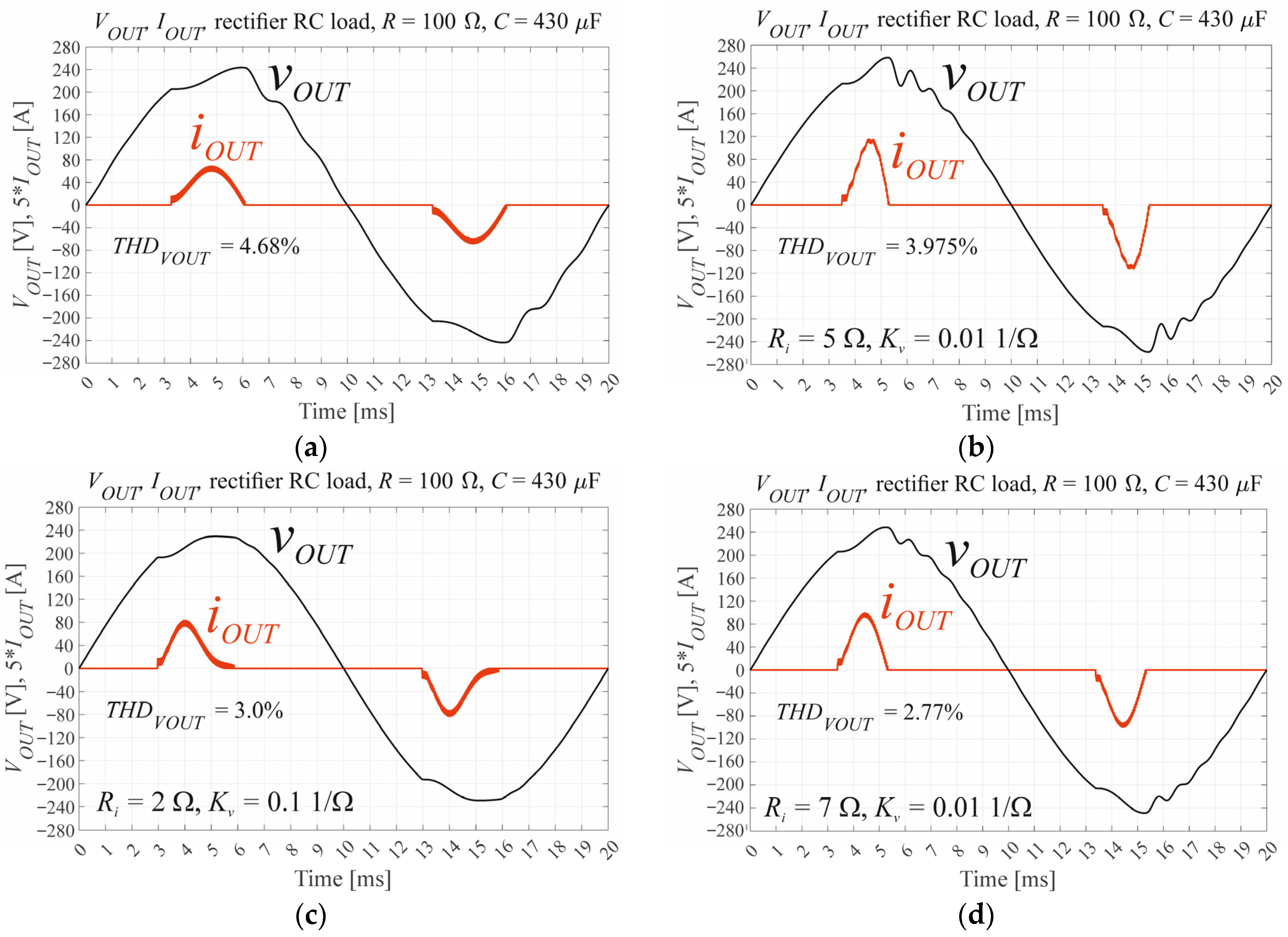
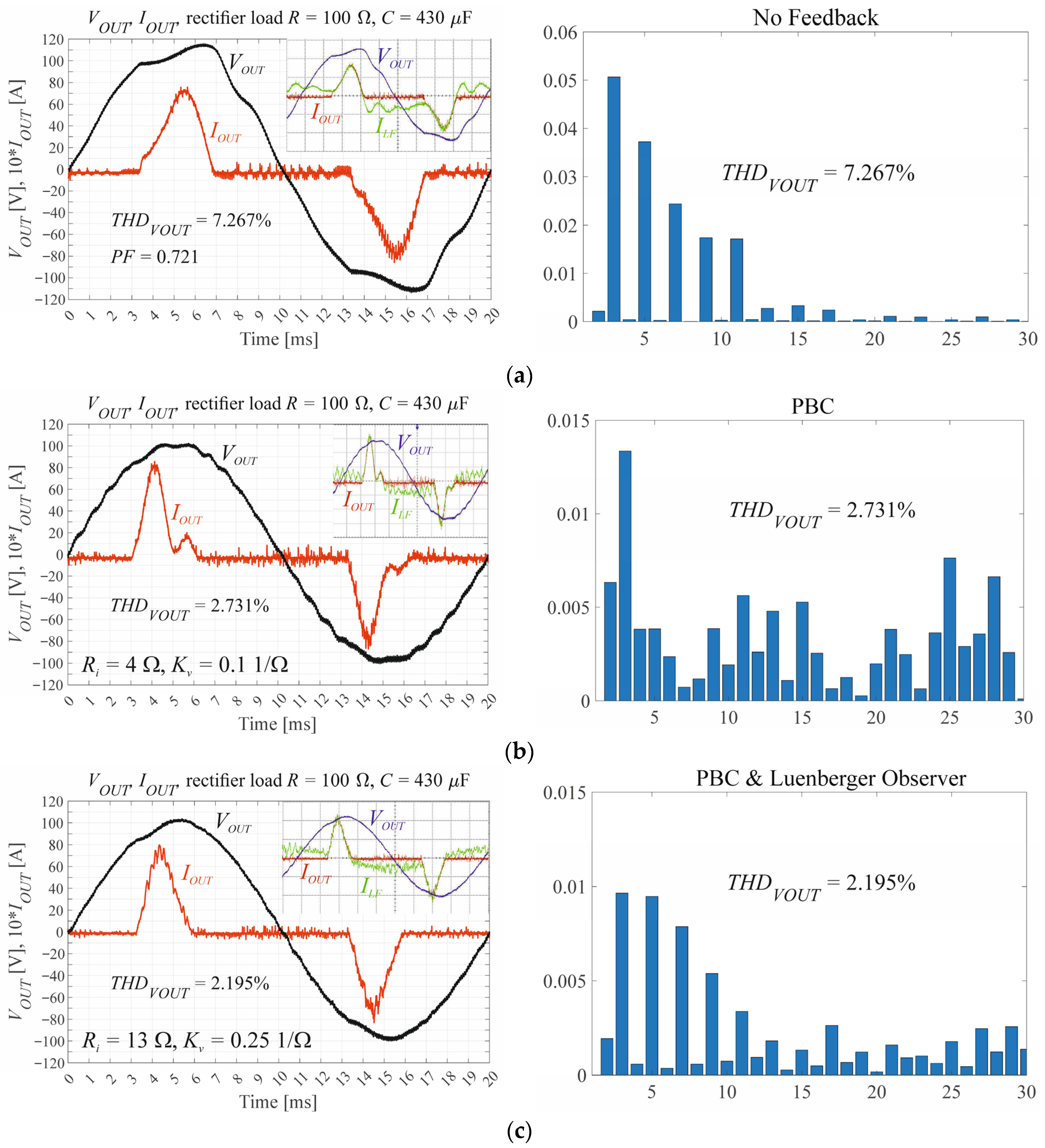
8. Comparison of the Simulation Results

Figure 10 presents the results of the prediction in the control of the low switching frequency VSI. The results of using the Luenberger observer and the linear Kalman filter are almost the same. In both cases, the gains of controller Ri and Kv were adjusted to get the lowest output voltage distortions defined by the THD coefficient. The final decision was to use the Luenberger observer because it is much easier to realise in microprocessor software than the recursive Kalman filter where there are a lot of matrix operations.

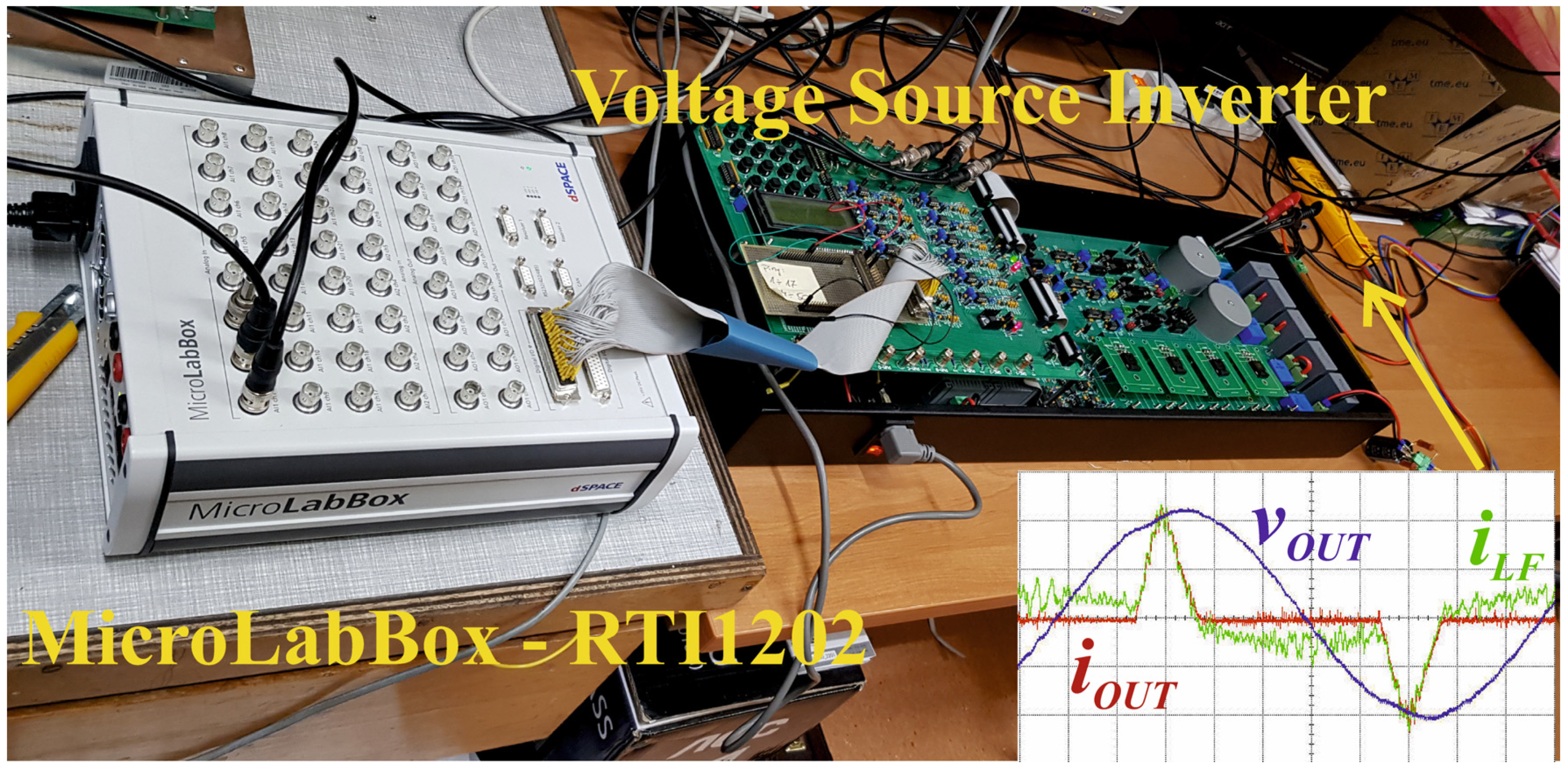
9. Breadboard Verifications of the Simulations

The presented problem of PBC control for the low switching frequency was experimentally checked. The example of control for the high switching frequency (51,200 Hz) where no prediction was necessary was presented in [17]. In all the cases, the maximum (without oscillations) gains Ri and Kv were set after initial adjustment based on Figure 6. It was noticed that the area of the stable operation is as in Figure 6 but the voltage gain Kv requires additional restriction. The fastest way to conduct the experimental verification was to use the Real Time Interface for MATLAB/Simulink 2021b, e.g., RTI1202 MicroLabBox with dSpace libraries for Simulink [17,41]. Scaling the gain of the measurement traces is a very important but often neglected problem [41]. In the case of RTI1202, it is easy to use dSpace Control Panel 7.5. For the open loop, for the nominal output voltage and the assigned resistive load, we set the gains in Simulink to get equal amplitude values for all of the voltage and current waveforms. Further, both current values were divided by the value of the existing resistive load (Figure 11). Each of the 3 independent ADCs were triggered by PWM events. The first ADC channel 1 interruption, when data are ready, calls the whole function block, which is seen in Figure 11. The PBC controller directly realises control laws (14) and (15). The predictor from Figure 11 realises Equation (19). The modulation scheme is from Figure 2. The compiled file is transmitted to MicroLabBox which measures the output voltage, output current and inductor current signals and drives two legs of the H-bridge described in Section 2.3.
The experimental VSI output voltage and harmonics spectrum without control (Figure 12a), with PBC control without prediction (Figure 12b) and with PBC control and prediction with the full state Luenberger observer (Figure 12c) are presented. The gains Ri and Kv for the PBC controller without predictor were adjusted to 4 and 0.1, respectively, to get the lowest distortion of the output voltage without oscillations. The higher values of the gains caused output voltage oscillations. For the system with a predictor, it was possible to increase the gains Ri and Kv to 13 and 0.25, respectively, without oscillations. The Luenberger observer l1, l2 and l3 gains were set to 1, 1 and 0.5, respectively. The laboratory VSI controlled with the MicroLabBox is shown in Figure 13.

10. Results

The results of the simulated and experimental research are presented in Table 1. The linear Kalman filter was only simulated because the distortions of the output voltage were very similar to the results of using the full-state Luenberger observer while the complexity of the calculations is much higher (the matrix operations). For the open loop, the THDVOUT of the experimental inverter was higher than in simulations because the additional output voltage ripple was included in the calculations. In the case of PBC feedback with or without a predictor, THDVOUT was lower for the experimental VSI because the real delay can be slightly lower than assigned in simulations. The current Ri and voltage gains Kv were, in each case, set to the maximum values that resulted in the lowest output voltage distortions without noticeable oscillations.

11. Discussion

The presented simulations and measurements of the experimental model controlled by the RTI1202 (MicroLabBox) showed that the measurement traces can be modelled as the simple delay and using the prediction can decrease the output voltage distortions. In this research, the full-state Luenberger observer of the measured output voltage, output current and inductor current was used and compared in simulations with the linear Kalman filter, used for state variables prediction. With almost the same results, the Luenberger observer was chosen for the experimental verification. The output voltage waveforms are presented in Figure 10 and Figure 12. The results of the simulation and experimental verification were compared in Table 1. An additional estimation for the solutions used can be performed based on the harmonics spectrum for each case from Figure 12. The PBC controller with the Luenberger observer reduces harmonics four to five times (Figure 12c vs. Figure 12a). The PBC controller without predictor reduced some low-frequency harmonics but increased some of the harmonics, including the particularly disadvantageous even harmonics that change the symmetry of the waveform in the fundamental period.
The current and voltage maximum gains (without output voltage oscillations) were possibly highest for the usage of the Luenberger observer, which reduces the distortions in this case. However, all of their sets are from the operating area presented in Figure 6. The strong restriction of the voltage gain (the higher Kv causes oscillations) can be an aim of further discussion but it can possibly be a result of the scaling of the measurement traces.
The gains of the Luenberger observer were chosen from the allowable area presented in Figure 7 and Equation (26). The low output voltage distortions seen with the use of the Luenberger observer testify that the observer has faster dynamics than the inverter.

12. Conclusions

The presented research showed the utility of using the full-state Luenberger observer to predict the state variables when a simple delay can model the measurement traces in the case of a low switching frequency (e.g., 12,800 Hz). Using the Kalman filter requires very complex matrix calculations and the output voltage distortions are almost the same as for the Luenberger observer. In the previous research in [17], it was shown that the state variable predictions have no utility for the high switching frequency (e.g., 51,200 Hz). Now, all of the three state variable measurements were used in the predictor and as a result of this, the gains of the Luenberger observer could be higher, resulting in the possibly faster dynamics of the Luenberger observer than the dynamics of the plant (the inverter). The presented research should help in the design of the low switching frequency VSI controlled by the microprocessor system when measurement traces can be modelled as a simple delay in the low-frequency range. The delays of the measurement channels in the control without the prediction can cause an asymmetry of the fundamental period owing to the existing even harmonics in the spectrum of the output voltage (Figure 12b). The prediction of the state variables enables an increase in the gains of the PBC controller (Table 1), approximately up to the border of the stable area (Figure 6) for the used switching frequency, and seriously decreases the distortions of the VSI output voltage for the standard (IEC 62040 [3]) load.

Funding

The author was supported by a pro-quality grant from the Rector of the Silesian University of Technology, Zbigniew Rymarski, grant number: 02/140/RGJ24/0033. This research was partially supported by the Polish Ministry of Education and Science funding for statutory activities (BK-250/RAU11/2024).

Data Availability Statement

All data files with results of simulations and measurements, the software for VSI simulation and control of the experimental inverter are in the private possession of the author.

Acknowledgments

The author would like to thank Andrzej Tutaj, of Technika Obliczeniowa sp. z o. o. (www.tobl.com.pl) (accessed on 10 March 2024) for his support in the utilization of MicroLabBox, and Krzysztof Bernacki, Department of Electronics, Electrical Engineering and Microelectronics, Faculty of Automatic Control, Electronics and Computer Science, Silesian University of Technology, Gliwice, Poland, for his previous cooperation in inverter control research and his participation in the power electronics laboratory creation.

Conflicts of Interest

The author declares no conflicts of interest.

References

  1. IEC 62040-3:2021; Uninterruptible Power Systems (UPS)—Part 3: Method of Specifying the Performance and Test Requirements. IEC: Geneva, Switzerland, 2021.
  2. Akagi, H.; Watanabe, E.H.; Aredes, M. Instantaneous Power Theory and Applications to Power Conditioning; Wiley-IEEE Press: New York, NY, USA, 2007. [Google Scholar]
  3. IEEE 519-2022; IEEE Standard for Harmonic Control in Electric Power Systems. IEEE: New York, NY, USA, 2022.
  4. Cheng, X.; Chen, Y.; Chen, X.; Zhang, B.; Qiu, D. An extended analytical approach for obtaining the steady-state periodic solutions of SPWM single-phase inverters. In Proceedings of the IEEE Energy Conversion Congress and Exposition (ECCE), Cincinnati, OH, USA, 24 August 2017; pp. 1311–1316. [Google Scholar] [CrossRef]
  5. Cheng, Y.; Zha, X.; Liu, Y. Nonlinear modeling of inverter using the Hammerstein’s approach. In Proceedings of the INTELEC 2009—31st International Telecommunications Energy Conference, Incheon, Republic of Korea, 18–22 October 2009; pp. 1–4. [Google Scholar] [CrossRef]
  6. Kawamura, A.; Chuarayapratip, R.; Haneyoshi, T. Deadbeat control of PWM inverter with modified pulse patterns for uninterruptible power supply. IEEE Trans. Ind. Electron. 1988, 35, 295–300. [Google Scholar] [CrossRef]
  7. Blachuta, M.; Rymarski, Z.; Bieda, R.; Bernacki, K.; Grygiel, R. Continuous-time approach to discrete-time PID Control for UPS inverters—A case study. In Proceedings of the Asian Conference on Intelligent Information and Database Systems (ACIIDS), Phuket, Thailand, 23–26 March 2020; pp. 1–12. [Google Scholar]
  8. Ben-Brahim, L.; Yokoyama, T.; Kawamura, A. Digital control for UPS inverters. In Proceedings of the Fifth International Conference on Power Electronics and Drive Systems (PEDS 2003), Singapore, 17–20 November 2003; Volume 2, pp. 1252–1257. [Google Scholar]
  9. Deng, H.; Srinivasan, D.; Oruganti, R. Modeling and control of single-phase UPS inverters: A survey. In Proceedings of the International Conference on Power Electronics and Drives Systems (PEDS 2005), Kuala Lumpur, Malaysia, 28 November–1 December 2005; pp. 848–853. [Google Scholar]
  10. Dou, X.; Yang, K.; Quan, X.; Hu, Q.; Wu, Z.; Zhao, B.; Li, P.; Zhang, S.; Jiao, Y. An Optimal PR Control Strategy with Load Current Observer for a Three-Phase Voltage Source Inverter. Energies 2015, 8, 7542–7562. [Google Scholar] [CrossRef]
  11. Borsalani, J.; Dastfan, A. Decoupled phase voltages control of three phase four-leg voltage source inverter via state feedback. In Proceedings of the 2012 2nd International eConference on Computer and Knowledge Engineering (ICCKE), Mashhad, Iran, 18–19 October 2012; pp. 71–76. [Google Scholar] [CrossRef]
  12. Moon, S.; Choe, J.M.; Lai, J.S. Design of a state-space controller employing a deadbeat state observer for ups inverters. In Proceedings of the 2017 Asian Conference on Energy, Power and Transportation Electrification (ACEPT), Singapore, 24–26 October 2017; pp. 1–6. [Google Scholar] [CrossRef]
  13. Hu, C.; Wang, Y.; Luo, S.; Zhang, F. State-space model of an inverter-based micro-grid. In Proceedings of the 2018 3rd International Conference on Intelligent Green Building and Smart Grid (IGBSG), Yilan, Taiwan, 22–25 April 2018; pp. 1–7. [Google Scholar] [CrossRef]
  14. Rymarski, Z. The discrete model of the power stage of the voltage source inverter for UPS. Int. J. Electron. 2011, 98, 1291–1304. [Google Scholar] [CrossRef]
  15. Rymarski, Z.; Bernacki, K. Different approaches to modelling single-phase voltage source inverters for uninterruptible power supply systems. IET Power Electron. 2016, 9, 1513–1520. [Google Scholar] [CrossRef]
  16. Rymarski, Z.; Bernacki, K. Different Features of Control Systems for Single-Phase Voltage Source Inverters. Energies 2020, 13, 4100. [Google Scholar] [CrossRef]
  17. Rymarski, Z. Simple Discrete Control of a Single-Phase Voltage Source Inverter in a UPS System for Low Switching Frequency. Energies 2023, 16, 5717. [Google Scholar] [CrossRef]
  18. Ortega, R.; Perez, J.A.L.; Nicklasson, P.J.; Sira-Ramirez, H. Passivity-Based Control of Euler-Lagrange Systems: Mechanical, Electrical and Electromechanical Applications (Communications and Control Engineering); Springer: London, UK, 1998. [Google Scholar]
  19. Wang, Z.; Goldsmith, P. Modified energy-balancing-based control for the tracking problem. IET Control Theory Appl. 2008, 2, 310–312. [Google Scholar] [CrossRef]
  20. Ortega, R.; Garcia-Canseco, E. Interconnection and Damping Assignment Passivity-Based Control: A Survey. Eur. J. Control 2004, 5, 432–450. [Google Scholar] [CrossRef]
  21. Ortega, R.; Garcia-Canseco, E. Interconnection and Damping Assignment Passivity-Based Control: Towards a Constructive Procedure—Part I. In Proceedings of the 43rd IEEE Conference on Decision and Control, Nassau, Bahamas, 14–17 December 2004; pp. 3412–3417. [Google Scholar] [CrossRef]
  22. Ortega, R.; Espinosa-Perez, G. Passivity-based control with simultaneous energy-shaping and damping injection: The induction motor case study. IFAC Proc. Vol. 2005, 38, 477–482. [Google Scholar] [CrossRef]
  23. Komurcugil, H. Improved passivity-based control method and its robustness analysis for single-phase uninterruptible power supply inverters. IET Power Electron. 2015, 8, 1558–1570. [Google Scholar] [CrossRef]
  24. Serra, F.M.; De Angelo, C.H.; Forchetti, D.G. IDA-PBC control of a DC-AC converter for sinusoidal three-phase voltage generation. Int. J. Electron. 2017, 104, 93–110. [Google Scholar] [CrossRef]
  25. Khefifi, N.; Houari, A.; Ait-Ahmed, M.; Machmoum, M.; Ghanes, M. Robust IDA-PBC based Load Voltage Controller for Power Quality Enhancement of Standalone Microgrids. In Proceedings of the IEEE IECON 2018—44th Annual Conference of the IEEE Industrial Electronics Society, Washington, DC, USA, 21–23 October 2018; pp. 249–254. [Google Scholar] [CrossRef]
  26. Ali, M.S.; Hou, Z.K.; Noori, M.N. Stability and performance of feedback control systems with time delays. Comput. Struct. 1998, 66, 241–248. [Google Scholar] [CrossRef]
  27. Mousa-Abadian, M.; Momeni-Masuleh, S.H.; Haeri, M. Stabilization of linear time-delayed systems by delayed feedback. Comput. Methods Differ. Equ. 2019, 7, 302–318. Available online: https://cmde.tabrizu.ac.ir/article_8553.html (accessed on 9 April 2024).
  28. Deng, Y.; Léchappé, V.; Moulay, E.; Chen, Z.; Liang, B.; Plestan, F.; Han, Q.L. Predictor-based control of time-delay systems: A survey. Int. J. Syst. Sci. 2022, 53, 2496–2534. [Google Scholar] [CrossRef]
  29. Gomez, M.; You, S.; Murray, R.M.; Time-Delayed Feedback Channel Design: Discrete Time H∞ Approach. 2014 American Control Conference (ACC). Available online: http://www.cds.caltech.edu/~murray/papers/gym14-acc.html (accessed on 10 March 2024).
  30. Sipahi, R.; Niculescu, S.I.; Abdallah, C.; Michiels, W.; Gu, K. Stability and Stabilization of Systems with Time Delay. IEEE Control Syst. Mag. 2011, 31, 38–65. [Google Scholar] [CrossRef]
  31. Van der Broeck, H.W.; Miller, M. Harmonics in DC to AC converters of single-phase uninterruptible power supplies. In Proceedings of the 17th International Telecommunications Energy Conference 1995 (INTELEC’ 95), The Hague, The Netherlands, 29 October–1 November 1995; pp. 653–658. [Google Scholar]
  32. Dahono, P.A.; Purwadi, A.; Qamaruzzaman. An LC filter design method for single-phase PWM inverters. In Proceedings of the International Conference on Power Electronics and Drive System, Singapore, 21–24 February 1995; Volume 2, pp. 571–576. [Google Scholar]
  33. Kim, J.; Choi, J.; Hong, H. Output LC filter design of voltage source inverter considering the performance of controller. In Proceedings of the International Conference on Power System Technology, Perth, WA, Australia, 4–7 December 2000; Volume 3, pp. 1659–1664. [Google Scholar]
  34. Ryu, B.; Kim, J.; Choi, J.; Choi, C. Design and analysis of output filter for 3-phase UPS inverter. In Proceedings of the Power Conversion Conference, Osaka, Japan, 2–5 April 2002; Volume 3, pp. 941–946. [Google Scholar]
  35. Film Capacitors, General Technical Information, June 2018, TDK. Available online: https://www.tdk-electronics.tdk.com/download/530754/480aeb04c789e45ef5bb9681513474ba/pdf-generaltechnicalinformation.pdf (accessed on 10 March 2024).
  36. Film Capacitors, Metallized Polypropylene Film Capacitors (MKP), June 2018, TDK. Available online: https://www.tdk-electronics.tdk.com/download/530784/62611300653ac1ee6053a0b5b4b5c37c/pdf-mkpoverview.pdf (accessed on 10 March 2024).
  37. Micrometals Alloy Powder Core Catalog. 2021. Available online: https://www.micrometals.com/design-and-applications/literature/ (accessed on 10 March 2024).
  38. Bernacki, K.; Rymarski, Z.; Dyga, Ł. Selecting the coil core powder material for the output filter of a voltage source inverter. Electron. Lett. 2017, 53, 1068–1069. [Google Scholar] [CrossRef]
  39. Bertotti, G. General properties of power losses in soft ferromagnetic materials. IEEE Trans. Magn. 1988, 24, 621–630. [Google Scholar] [CrossRef]
  40. Rymarski, Z. Measuring the real parameters of single-phase voltage source inverters for UPS systems. Int. J. Electron. 2017, 104, 1020–1033. [Google Scholar] [CrossRef]
  41. Bernacki, K.; Rymarski, Z. A Contemporary Design Process for Single-Phase Voltage Source Inverter Control Systems. Sensors 2022, 22, 7211. [Google Scholar] [CrossRef]
  42. Luenberger, D.G. Observing the state of a linear system. IEEE Trans. Mil. Electron. 1964, 8, 74–80. [Google Scholar] [CrossRef]
  43. Luenberger, D.G. An introduction to observers. IEEE Trans. Autom. Control 1971, 16, 596–602. [Google Scholar] [CrossRef]
  44. Davis, J.H. Luenberger Observers. In Foundations of Deterministic and Stochastic Control. Systems & Control: Foundations & Applications; Birkhäuser: Boston, MA, USA, 2002; pp. 245–254. [Google Scholar] [CrossRef]
  45. Montagner, V.F.; Carati, E.G.; Grundling, H.A. An adaptive linear quadratic regulator with repetitive controller applied to uninterruptible power supplies. In Proceedings of the Industry Applications Conference 2000, Rome, Italy, 8–12 October 2000; Volume 4, pp. 2231–2236. [Google Scholar]
  46. Saoudi, M.; Hani, B.; Aissa, C. Efficient Deadbeat Control of Single-Phase Inverter with Observer for High Performance Applications. Prz. Elektrotechniczny 2023, 99, 237. [Google Scholar] [CrossRef]
  47. Fan, H.; Li, Z.; Rodriguez, J.; Wang, B. Model Free Predictive Current Control for Voltage Source Inverter using Luenberger Observer. In Proceedings of the 2023 IEEE International Conference on Predictive Control of Electrical Drives and Power Electronics (PRECEDE), Wuhan, China, 16–19 June 2023; pp. 1–6. [Google Scholar] [CrossRef]
  48. Heydaridoostabad, H.; Ghazi, R. A new approach to design an observer for load current of UPS based on Fourier series theory in model predictive control system. Int. J. Electr. Power Energy Syst. 2018, 104, 898–909. [Google Scholar] [CrossRef]
  49. Kalman, R.E. New methods and results in linear prediction and filtering theory. In Proceedings of the Symposium on Engineering Applications of Random Function Theory and Probability; Bogdanoff, J.L., Kozin, F., Eds.; Wiley: New York, NY, USA, 1961; pp. 270–388. [Google Scholar]
  50. Grewal, M.S.; Andrews, A.P. Kalman Filtering. Theory and Practice Using MATLAB; John Wiley & Sons, Inc.: Hoboken, NJ, USA, 2008. [Google Scholar]
  51. Franklin, G.F.; Powell, J.D.; Workman, M.L. Digital Control of Dynamic Systems, 2nd ed.; Addison-Wesley: New York, NY, USA, 1990. [Google Scholar]
  52. Dróżdż, K. Identification of mechanical parameters of the two-mass system using fuzzy Kalman filter. In Scientific Papers of The Institute of Electrical Machines, Drives and Measurements of the Wrocław University of Science and Technology Series: Studies and Research; Wrocław University of Science and Technology: Wrocław, Poland, 2013; Volume 69, pp. 156–169. ISSN 1733-0718. [Google Scholar]
  53. Chen, B.; Wu, W.; NGao Yao, Z.; Chung, H.; Blaabjerg, F. Kalman-Filter-Estimation Based Sliding Mode Control of Three-Phase LCL-Filtered Grid-Tied Inverter Using only Grid-Injected Current Sensors. In Proceedings of the 2020 IEEE 9th International Power Electronics and Motion Control Conference (IPEMC2020-ECCE Asia), Nanjing, China, 29 November–2 December 2020; pp. 2368–2373. [Google Scholar] [CrossRef]
  54. Gao, C. A New Control Method with Simplified Model and Kalman Filter Estimator for Grid-Tied Inverter with Asymmetric LCL Filter. Authorea 2023. [Google Scholar] [CrossRef]
Figure 1. Single-phase MISO VSI control described in the paper.
Electronics 13 01469 g001
Figure 2. The idea of driving H-bridge transistors in the 1-scheme of PWM.
Electronics 13 01469 g002
Figure 3. The increase in the simulated PWM output voltage THD caused by dead time.
Electronics 13 01469 g003
Figure 4. Measuring the Bode plots of the output voltage channel.
Electronics 13 01469 g004
Figure 5. The Bode plots of two VSIs’ measurement traces and their approximation. (a,b) The first VSI, approximation function: exp(−jω3Ts). (c,d) The second VSI, approximation function: exp(−jω2Ts).
Electronics 13 01469 g005aElectronics 13 01469 g005b
Figure 6. Operating area of PBC (a) for different switching frequencies and filter induction LF and (b) for the assigned output filter parameters.
Electronics 13 01469 g006
Figure 7. The allowable values of l1 and l2 for fs =12,800 Hz, LF = 1 mH and CF = 51 μF.
Electronics 13 01469 g007
Figure 8. The MATLAB/Simulink model of the low switching frequency VSI with prediction with the Luenberger observer and modelled delays in the measurement traces.
Electronics 13 01469 g008
Figure 9. The MATLAB/Simulink model of the low switching frequency VSI with prediction with the linear Kalman filter. The Q, R and N matrixes of the Kalman filter and the VSI discrete model matrixes A, B and C are in the right side of the figure.
Electronics 13 01469 g009
Figure 10. Comparison between distortions of the output voltage (a) for an open loop; (b) for the PBC without prediction; (c) for the PBC and the Luenberger prediction and (d) for the PBC and the linear Kalman filter.
Electronics 13 01469 g010
Figure 11. The schema of the control system transmitted to the MicroLabBox (version with the predictor). The PBC controller and the predictor are grey (assembled from standard Simulink blocks). Multichannel PWM and ADC blocks are from dSpace library.
Electronics 13 01469 g011
Figure 12. The VSI output voltage and current for fs = 12,800 Hz, RL = 1 Ω, LF = 1 mH, CF = 51 μF, rectifier load R = 100 Ω, C = 430 μF, (a) for the open loop, (b) for PBC controller without prediction and (c) for PBC controller with prediction.
Electronics 13 01469 g012
Figure 13. The experimental laboratory VSI.
Electronics 13 01469 g013
Table 1. THDVOUT of the output voltage of the simulated and experimental VSI for fs = 12,800 Hz, RL = 1 Ω, LF = 1 mH, CF = 51 μF, rectifier load R = 100 Ω, C = 430 μF. There was not experimental verification of the prediction with the Kalman filter.
Simulation VSI
Rimax, Kvmax
Simulation VSI THDVOUTExperimental
Rimax, Kvmax
Experimental VSI THDVOUT
No feedbacknone4.68%none7.27%
PBC controllerRimax = 5, Kvmax = 0.013.98%Rimax = 4, Kvmax = 0.12.73%
PBC controller with the full-state Luenberger observerRimax = 2, Kvmax = 0.1,
l1 = 1, l2 = 1, l3 = 0.5
3.0%Rimax = 13, Kvmax = 0.25,
l1 = 1, l2 = 1, l3 = 0.5
2.20%
PBC controller with the linear Kalman filterRimax = 7, Kvmax = 0.012.77%not usednot checked
Disclaimer/Publisher’s Note: The statements, opinions and data contained in all publications are solely those of the individual author(s) and contributor(s) and not of MDPI and/or the editor(s). MDPI and/or the editor(s) disclaim responsibility for any injury to people or property resulting from any ideas, methods, instructions or products referred to in the content.

