Article

A 2.25 ppm/°C High-Order Temperature-Segmented Compensation Bandgap Reference

1
School of Integrated Circuits, University of Chinese Academy of Sciences, Beijing 101408, China
2
Institute of Microelectronics of the Chinese Academy of Sciences, Beijing 100029, China
*
Author to whom correspondence should be addressed.
Electronics 2024, 13(8), 1499; https://doi.org/10.3390/electronics13081499
Submission received: 6 January 2024 / Revised: 8 February 2024 / Accepted: 13 February 2024 / Published: 15 April 2024

Abstract

:
This paper presents a bandgap reference (BGR) with high-order temperature-segmented compensation. The compensation signal is generated using the voltage difference between two bipolar junction transistor (BJT) emitter bases, each of which individually loads a proportional-to-absolute temperature (PTAT) current and a zero-to-absolute temperature (ZTAT) current. The proposed BGR achieves a low-temperature coefficient (TC) over a wide temperature range. Simulations using the 0.18 μm Bipolar-CMOS-DMOS process show a typical TC of 2.25 ppm/°C from −40 °C to 125 °C. With an active area of 0.07986 mm2, it consumes 36 μW power under an operating voltage of 1 V. The integrated output noise from 0.1 Hz to 10 Hz is 81.1 μV.

1. Introduction

Bandgap reference (BGR) is an essential component in many analog, digital and mixed-signal integrated circuits. The output voltage of the traditional voltage-mode BGR is 1.25 V, which is approximately equal to the semiconductor material’s extrapolated energy bandgap voltage [1]. Due to the fixed output voltage, the minimum supply voltage for the traditional voltage-mode BGR would be around 1.5 V. Consequently, the traditional voltage-mode BGR [2,3] is not suitable for low-voltage applications. It is important to have a low-voltage and low-power PVT-insensitive reference circuit for battery-operated portable devices such as hearables and wearables. The current-mode BGR transforms the proportional-to-absolute temperature (PTAT) voltage and the complementary-to-absolute temperature (CTAT) voltage to a temperature-independent current to produce a temperature-independent bandgap voltage reference under 1.2 V, as proposed by H. Banba [4]. The minimum supply voltage for the current-mode BGR can be lower than 1.2 V. Current-mode BGRs are more flexible in output voltages [5], and various compensation methods for current-mode BGRs have been proposed.
Traditional bipolar junction transistor (BJT)-based BGRs with the first-order temperature compensation have typical temperature coefficients ranging from 20 ppm/°C to 100 ppm/°C [6]. To achieve high accuracy and stability over a wide temperature range, the high-order temperature compensation is used to eliminate the nonlinear component of the PN junction voltage. Various curvature compensation methods were proposed to enhance the accuracy and stability of low-voltage BGRs. For instance, Bill Ma and Fengqi Yu used metal oxide semiconductor (MOS) transistors operating in the weak inverse region, which have a positive second-order temperature coefficient opposite to BJTs [7], to compensate for high-order nonlinearity. In [8], a method based on multistage currents with different temperature thresholds was proposed to compensate for the temperature-dependent nonlinearity term. The scheme using the voltage difference between Veb at a PTAT current and Veb at a zero-to-absolute temperature (ZTAT) current was implemented to compensate for the high-order nonlinear term in Vbe [9]. However, this approach introduced additional high-order nonlinear currents. But the minimum supply voltage of BJT-based voltage reference cannot be lower than 0.7 V due to the presence of the BJT. To obtain a lower supply voltage, metal oxide semiconductor field effect transistors (MOSFETs) that operate in the subthreshold region are used instead of BJTs. Veb and ΔVeb are replaced by VGS and ΔVGS, respectively. Current-mode BGRs and current references (CRs) consisting only of MOSFETs were proposed [10,11,12]. A current reference based on a minimum current search principle implemented current compensation, which is similar to piecewise compensation, to improve the temperature coefficient [13]. Different topologies of MOSFET threshold-based voltage references are shown [14]. Although the threshold voltage-based reference can be used at lower supply voltages, it is more susceptible to variations in the CMOS fabrication process than the BJT-based reference [14]. In order to obtain a lower supply voltage, the low-threshold-voltage (LVT) or zero-threshold-voltage (ZVT) MOSFET was introduced [15].
In this paper, we present a low-voltage current-mode BGR with standard-threshold-voltage (SVT) MOSFETs implementing high-order temperature-segmented compensation. Two BJTs operating at PTAT currents and ZTAT currents, respectively, jointly generate a compensation signal. Unlike previous works, our design avoids additional high-order nonlinear currents when the ZTAT current flows into Veb. Additionally, our approach achieves the segmented compensation of the temperature curve.
The remainder of this paper is organized as follows: Section 2 explains the principle of high-order temperature compensation for the proposed BGR. Section 3 discusses the startup circuit. Section 4 presents the trimming and simulation results. Finally, Section 5 provides the conclusion.

2. Principle of High-Order Temperature Compensation

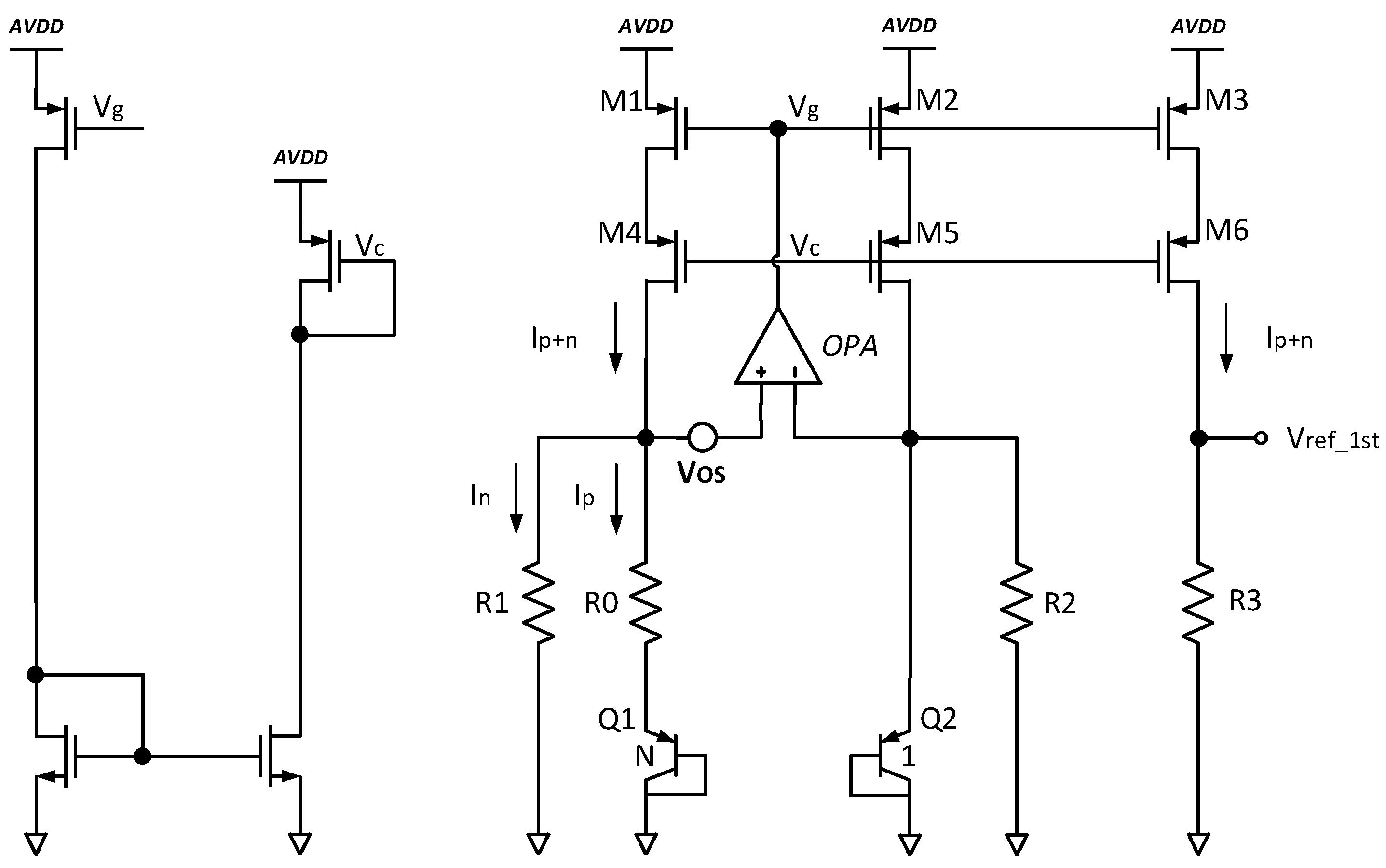
2.1. Traditional Low-Voltage BGR

The traditional low-voltage BGR achieves first-order temperature compensation by utilizing two components with opposite first-order temperature coefficients. On the one hand, the positive first-order temperature coefficient is provided by the voltage difference of two emitter-bases, ΔVeb, which both load PTAT currents. On the other hand, the negative first-order temperature coefficient is usually generated by the emitter-base voltage Veb. The traditional low-voltage current-mode BGR is shown in Figure 1. The PTAT voltage, ΔVeb, is converted into the PTAT current, Ip, by dividing the resistor R0. The CTAT voltage, Veb, is converted into the CTAT current, In, by dividing the resistor R1. The resistance of R2 is equal to R1. The current Ip+n, which is the sum of Ip and In, achieves first-order temperature compensation. Ip+n is multiplied by resistance, R3, and is converted to a reference voltage Vref_1st with first-order temperature compensation. The temperature characteristics are derived as follows.
The PTAT current Ip can be written as
  I p = V e b R 0 = V T ln N R 0 = k T ln N q R 0
where N is the ratio of emitter area of Q1 to Q2.
The CTAT current In can be written as
  I n = V e b Q 2 R 1
The temperature model of Veb can be expressed as the following expression:
V e b T = V g ( T ) V g ( T R ) V e b ( T R ) T T R η α V T ln T T R
where TR is the specified reference temperature, Vg(TR) is the bandgap voltage at TR, Veb(TR) is the emitter-base voltage at TR and η is a process-dependent constant around 4 [16]. α is equal to 1 when the BJT loads the PTAT current and equal to 0 when the BJT loads ZTAT current. Vg(T) is the bandgap voltage as a function of temperature.
  V g T = V g 0 b T c T 2
where Vg0 is 1.17885 V to 1.20595 V, b is 9.025 × 10⁻⁵ V/K to 2.7325 × 10⁻⁴ V/K and c is 3.05 × 10⁻⁷ V/K2 to 0 if the temperature is between 150 K and 400 K [17].
Therefore, the expression of Ip+n can be obtained.
I p + n = V T ln N R 0 + V e b Q 2 R 1
The expression of Vref_1st is formulated as
V r e f _ 1 s t = V T ln N R 0 + V e b Q 2 R 1 × R 3 = R 3 R 1 V g 0 + R 3 R 1 R 1 R 0 kln N q V g T R V e b Q 2 T R T R b T R 3 R 1 [ c T 2 + η α V T ln T T R ]
where VebQ2(TR) is the emitter-base voltage VebQ2 at TR.
Obviously, the traditional low-voltage BGR can achieve the first-order temperature compensation by eliminating the second term in (6). Therefore, the first-order temperature term can be easily eliminated by adjusting the ratio of the resistor R1 to R0 and the value of N to satisfy (7).
  R 1 R 0 l n N = q k ( V g T R V e b Q 2 T R T R + b )
Typically, Vref_1st presents a second-order parabola going downwards due to the presence of the third term in (6). Taking into account the trade-off between power consumption and the area of the circuit, the value of N is 13 in this work. In order to improve the power supply rejection ratio (PSRR) of the traditional low-voltage current-mode BGR, cascode current mirrors are used [18].

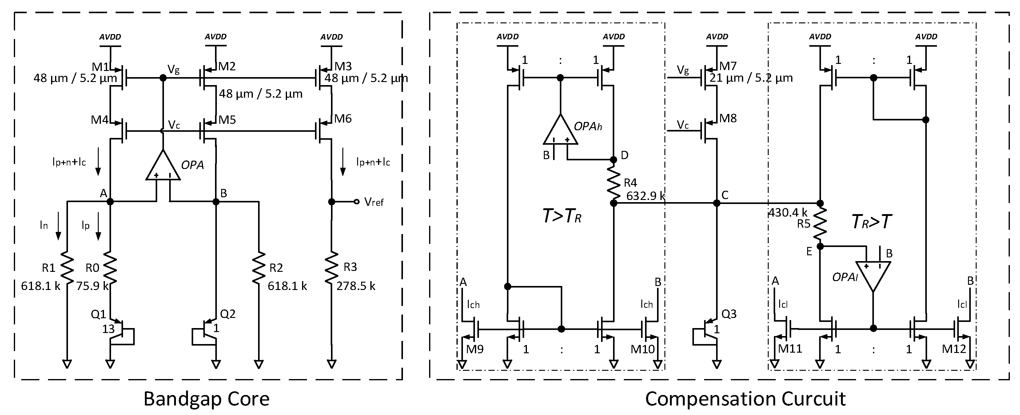
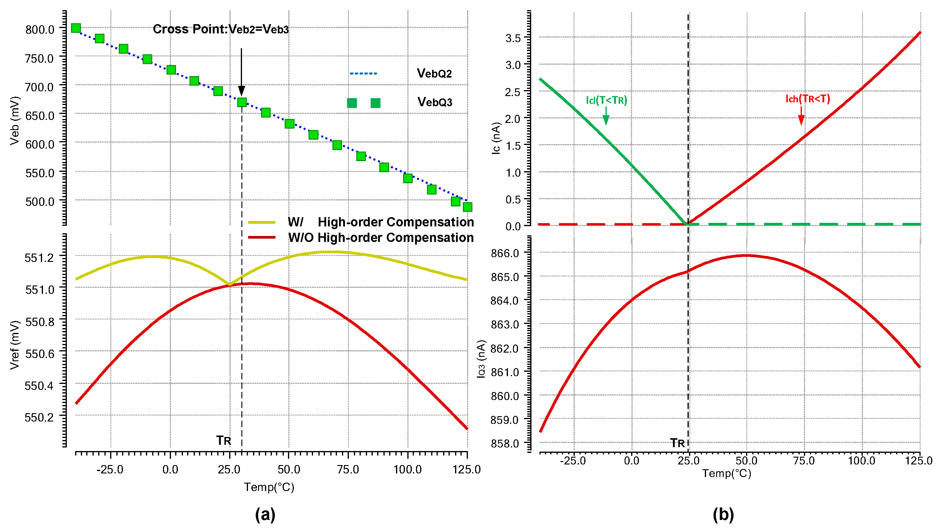
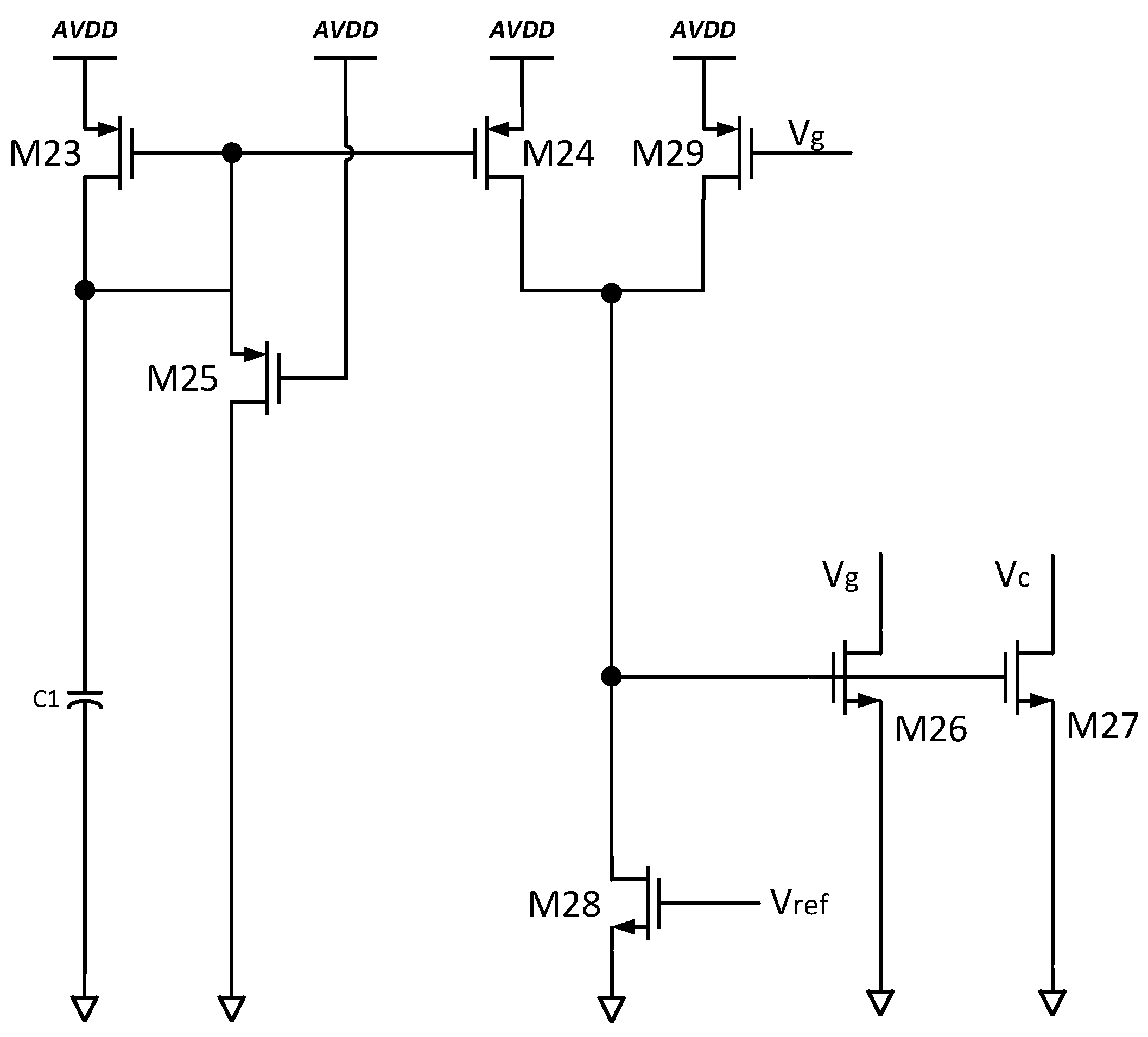
2.2. The Proposed Low-Voltage BGR

The curvature compensation method depicted in Figure 1 can realize the first-order temperature compensation. However, the presence of the third term in Equation (6) still causes Vref_1st to vary across the whole temperature range. In order to obtain a more stable reference voltage, it is necessary to suppress the influence of the nonlinear term in Equation (6). Various methods were proposed [19,20,21] to correct the nonlinear term. The basic ideas in [22,23] can be used in this scheme, as depicted in Figure 2.
Even without the presence of the high-order compensation circuit, the current through M7 mirrored from Ip+n is still a first-order temperature-compensated current. When the compensation circuit operates, the compensation current, Ic, is usually small in order to cancel the high-order nonlinear terms. Compared to the PTAT current or the CTAT current, Ip+n + Ic cannot change much with varying temperatures. To simplify calculations, the load current of Q3, IQ3, mirrored from M1 or M2, Ip+n + Ic, can be approximately regarded as a ZTAT current. The curve of IQ3 with varying temperatures is shown in Figure 3b. Therefore, the emitter-base voltage, VebQ3, of Q3 can be expressed by the following formula:
  V e b Q 3 T = V g ( T ) V g ( T R ) V e b Q 3 ( T R ) T T R η V T ln T T R
where VebQ3(TR) is the emitter-base voltage VebQ3 at TR.
The load current of Q2 is a PTAT current. Thus, the emitter-base voltage, VebQ2, of Q2 can be expressed as
  V e b Q 2 T = V g ( T ) V g ( T R ) V e b Q 2 ( T R ) T T R η 1 V T ln T T R
The expression of the compensation signal can be obtained by (8) and (9).
  V e b Q 2 T V e b Q 3 T = ( V e b Q 2 ( T R ) V e b 3 ( T R ) ) T T R + V T ln T T R
The second term in Equation (10) has the same expression form as the high-order nonlinear term in Equation (6). The first item in Equation (10) is the first-order term. Therefore, to achieve better compensation, the first item in Equation (10) will be eliminated. The following expression needs to be satisfied by adjusting the collector currents of Q3 and Q2.
  V e b Q 2 ( T R ) = V e b Q 3 ( T R )
Combining Equations (9) and (10), the intersection of VebQ3 and VebQ2 is obviously at TR. Curvature compensation is implemented, making the cross point of VebQ3 and VebQ2 located in the stationary point of the curve of Vref_1st, with the varying temperatures in Figure 3a.
When the temperature is higher than TR, VebQ2 is larger than VebQ3 in Figure 3a. In Figure 2, the right half of the circuit is the compensation circuit. VB = VebQ2 and VC = VebQ3 can be obtained. So, when the temperature is higher than TR, VB is larger than VC. And if the OPAl is working properly under such conditions, VE will be equal to VB. This will result in an unreasonable result where VE is greater than VC. Therefore, there is no current flowing through R5, resulting in VE being equal to VC. Since the positive input voltage of the OPAl is lower than the negative input voltage, the output voltage of the OPAl is low, resulting in zero load current flowing M11 and M12. However, the OPAh can work properly when the temperature is higher than TR. It can be obtained that VB = VD when OPAh can operate properly. The high-order compensation signal voltage, VTln(T/TR), is converted into a current through the resistor R4. Transistors M9 and M10 produce curvature compensation current Ich.
  I c h = k 4 V T ln T T R R 4
where k4 is the compensation current gain at high temperature. The higher the temperature, the greater the compensation current. In this work, the default value of k4 is 0.2.
When the temperature is lower than TR, the output voltage of the OPAh is high. The load current of M9 and M10 is zero. OPAl can work properly under low temperatures, and it can be obtained that VB = VE. The high-order compensation signal voltage, −VTln(T/TR), is converted into a current through the resistor R5. Therefore, when the temperature becomes lower than TR, transistors M11 and M12 produce a curvature compensation current Icl.
  I c l = k 5 V T ln T T R R 5
where k5 is the compensation current gain in a low-temperature scenario. The lower the temperature, the greater the compensation current. In this work, the default value of k5 is 0.25.
Vref_1st without high-order compensation presents a second-order parabola going downwards whose vertex is around TR, as shown in Figure 3a. As the temperature moves further away from TR, the voltage drops more. When the compensation circuit is active, the compensation current, Ic, which is the sum of Icl and Ich, appears as shown in Figure 3b. As the temperature moves further away from TR, the compensation current, Ic, increases more. The compensating current, Ic, flows through the resistor, R3, to cause a positive ΔVref and, thus, suppress the drop of Vref_1st. The smaller the Vref_1st, the larger the compensation current Ic. Therefore, the compensation curve for Vref displays a segmented compensation pattern, as shown in Figure 3a. Consequently, the segmented compensation has been successfully realized in this work. When Vref_1st is heavily affected by process and mismatch, Vref_1st may resemble a diagonal line. In such situations, TR needs to be set outside the temperature range, and Vref will exhibit a second-order parabolic behavior.

2.3. The Design of OPA
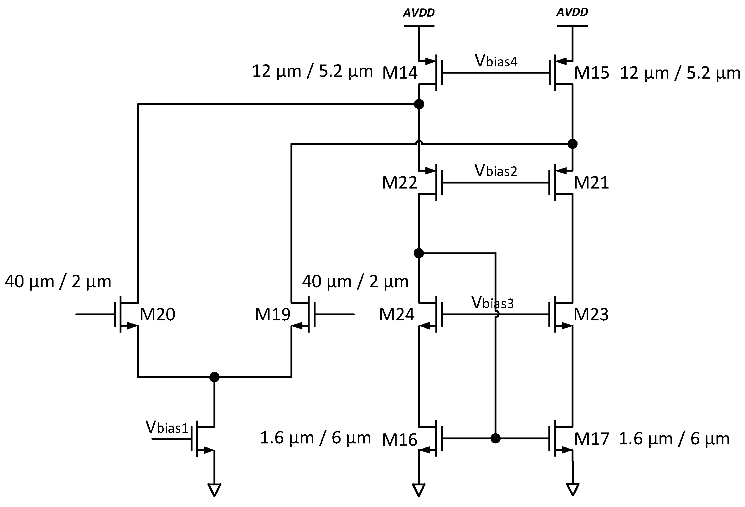
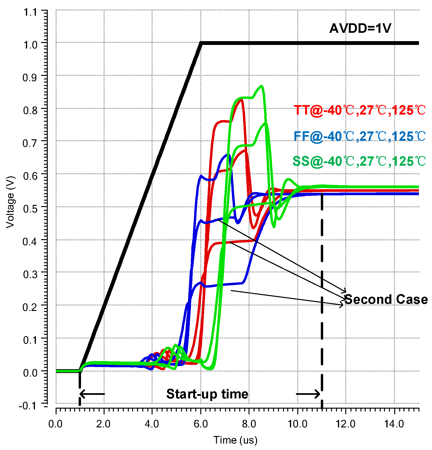
The operational amplifier (OPA) plays a crucial role in the proposed low-voltage BGR. One important parameter of the OPA is offset. The input offset of an OPA includes both systematic offset and random offset. Systemic offset arises due to the limited gain of the OPA. The higher gain in the OPA results in a smaller systematic input offset. Random offset, on the other hand, is caused by device mismatch. Increasing the chip area can help reduce mismatch, but this involves a trade-off between chip area and performance, as mentioned in reference [24].
It is evident that the input common-mode voltage of the OPA is Veb, which is between 800 mV and 500 mV from −40 °C to 125 °C. If PMOS differential input stages are used, the minimum supply voltage must meet the following formula: AVDDmin > |Vthp | + VDSp + Vebmax. As the supply voltage is approximately 1 V, the NMOS differential input stage is chosen instead of the PMOS differential input stage, and the minimum supply voltage is AVDDmin = 2VDSp + Vebmax ≈ 950 mV < 1 V, which is suitable for our design. 2VDSp, which is approximately 150 mV, represents the sum of the VDS of M2 and the VDS of M5 in Figure 2. In our process, the threshold voltage of the NMOS varies from 258 mV to 415 mV when W/L = 10 μm/10 μm and from 366 mV to 514 mV when W/L = 10 μm/0.18 μm, which satisfies the design requirements. The implementation of the OPA is illustrated in Figure 4.

3. Start-Up Circuit

The start-up circuit shown in Figure 5 is an important component of the BGR circuit. The BGR core circuit, depicted in Figure 1, can exist in three possible stable states. The first state occurs when the two arms of the BGR core circuit carry zero current. The currents Ip and In in Figure 1 are zero under the first state. The second state is characterized by a very small current flowing through R1 and R2, with Q1 and Q2 remaining inactive. Only the current Ip in Figure 1 is zero under the second state. The third state represents the desired operating state when the current in the two arms of the BGR core circuit matches the design value [25].
Upon powering on, the BGR core circuit initially enters the first state. Vref is zero, and transistor M28 is turned off. At this stage, transistor M23 begins to charge C1; meanwhile, transistor M24 charges the gate of transistors M26 and M27. Consequently, M26 and M27 turn on, resulting in Vg and Vc being pulled down. Currents begin to flow in the two arms of the BGR core circuit. Subsequently, the BGR core circuit may transition to the second state, where Vref is between the desired value and zero. Additionally, M28 turns on. To ensure the BGR core circuit exits the second state and reaches the expected stable state, M26 and M27 cannot be turned off. Therefore, it becomes necessary to introduce transistor M29 to continue charging the gates of M26 and M27. Once the circuit is functioning properly, Vref becomes sufficiently large to drive M28 into the linear region. Finally, M26 and M27 remain off. During power-off, transistor M25 is utilized to discharge the charge stored in C1. Figure 6 illustrates the simulated start-up waveforms of the proposed BGR.

4. Trimming and Simulation Results
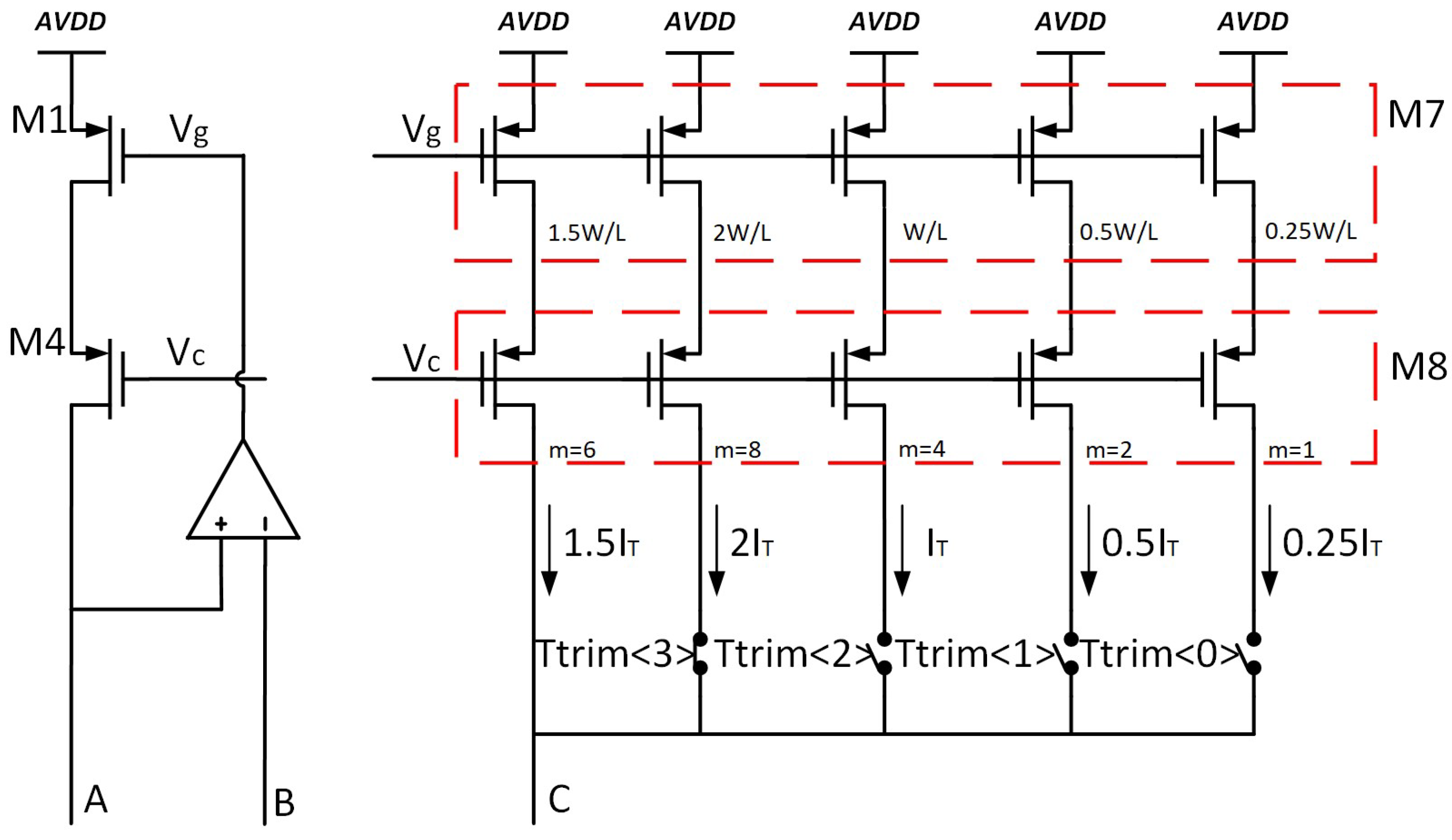
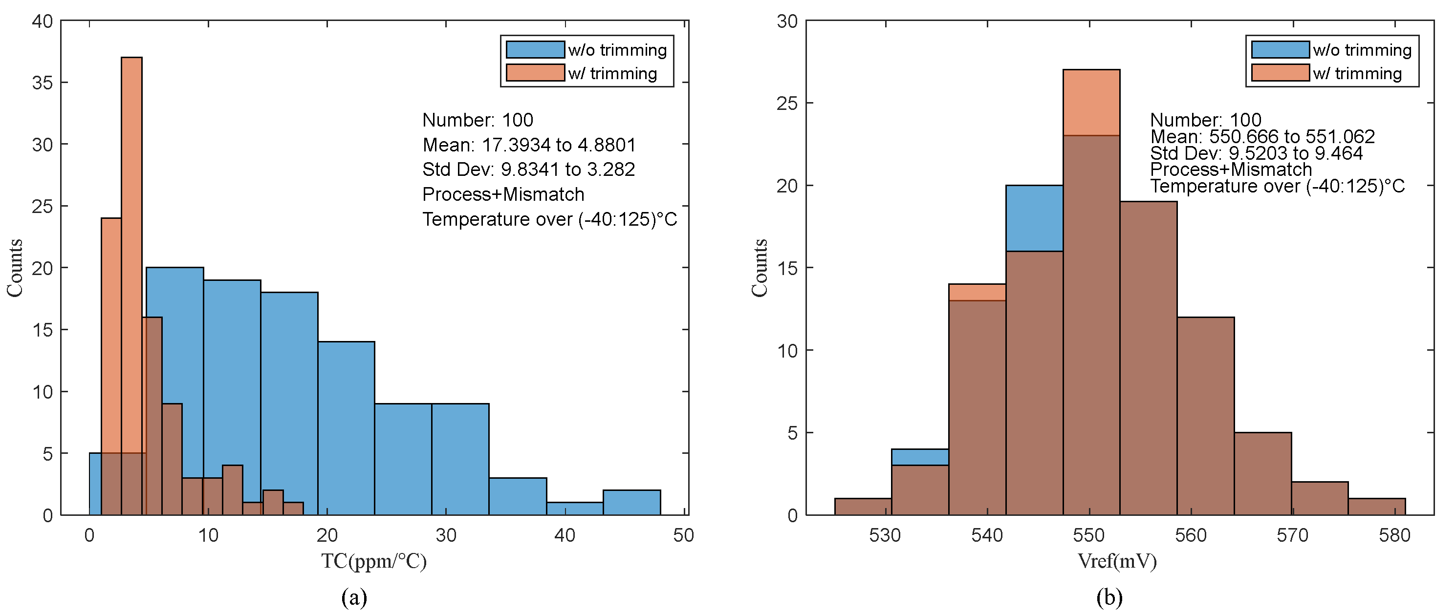
4.1. Trimming

Trimming at the wafer level is primarily designed to overcome process extensibility and random device variation during circuit manufacturing. The temperature trimming of the proposed BGR is mainly a high-order temperature trimming technique to achieve better temperature coefficient performance.
To realize high-order temperature compensation, (W/L)M7 should be adjusted so that the cross point of VebQ3 and VebQ2 is adjustable. As shown in Figure 7, the control word Ttrim<3:0> decides (W/L)M7, which changes the load current of Q3. The range of current variation is from −2IT to 1.75IT.
For high-order temperature trimming, the coefficients k4 and k5 are adjusted, as determined by Formulas (12) and (13). Similar to (W/L)M7, (W/L)M9–12 is used to adjust k4 and k5. In this work, K4trim<4:0> and K5trim<4:0> are utilized to adjust k4 and k5, respectively.

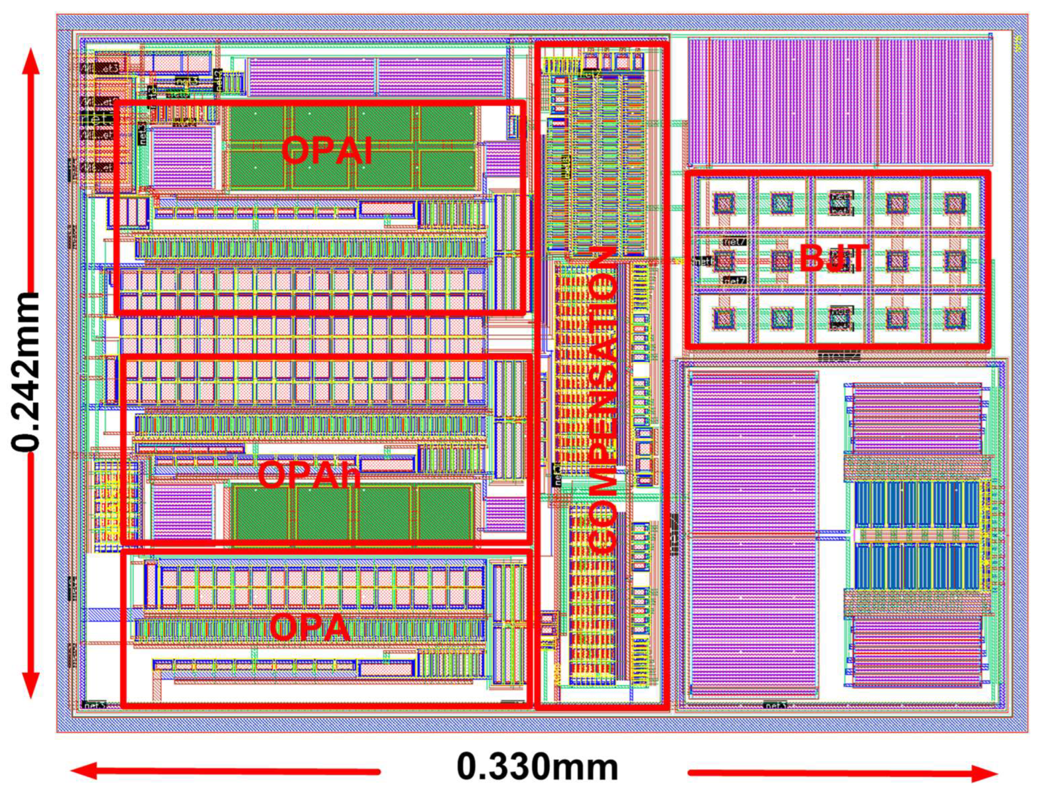
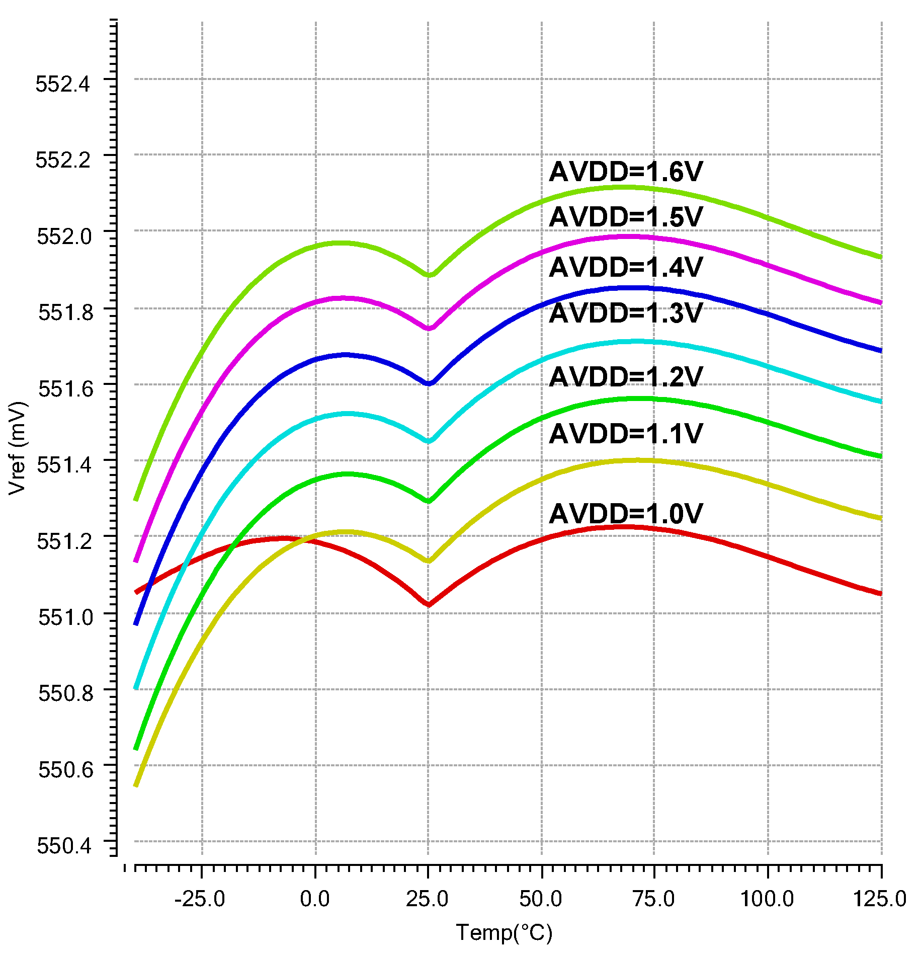
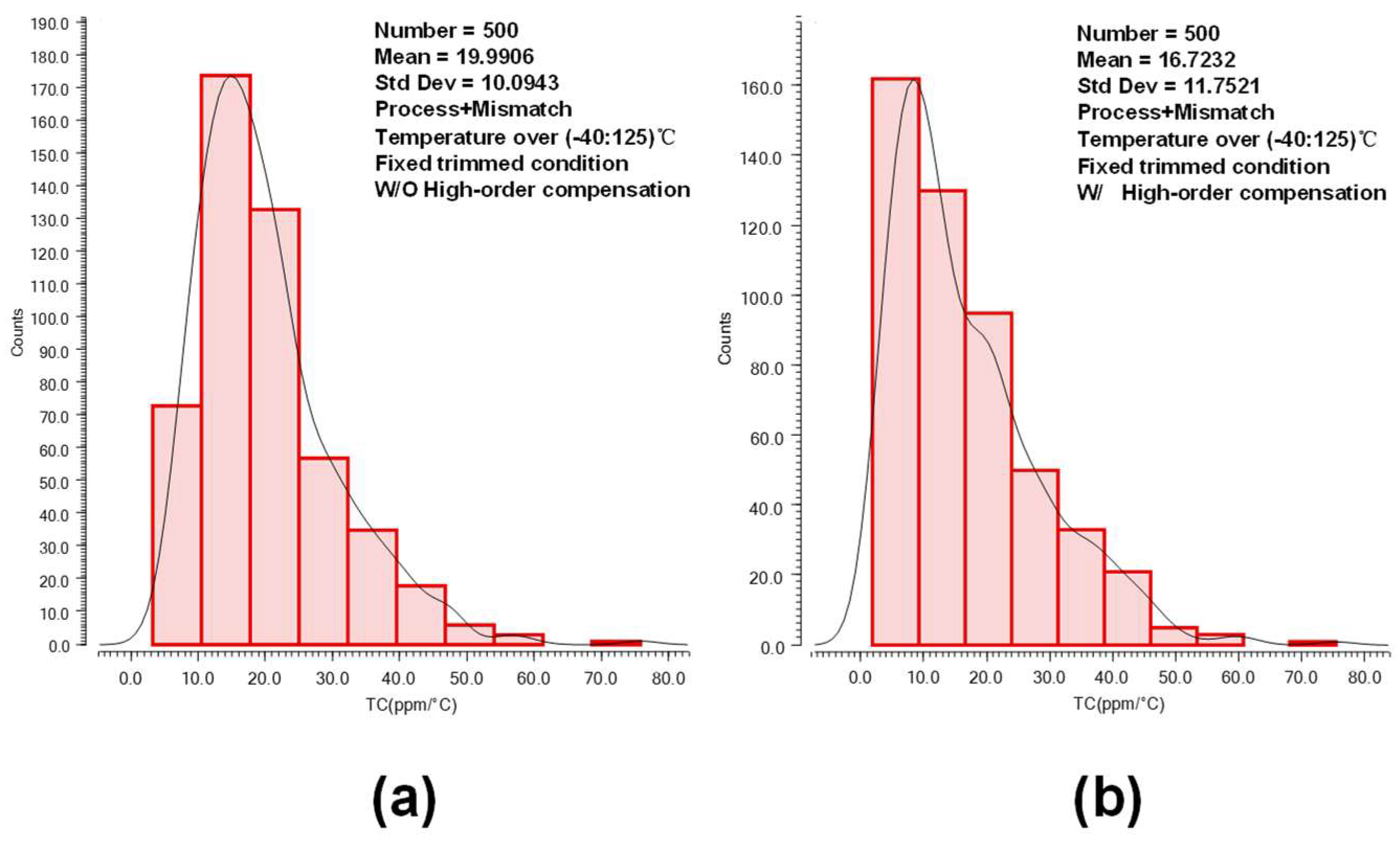
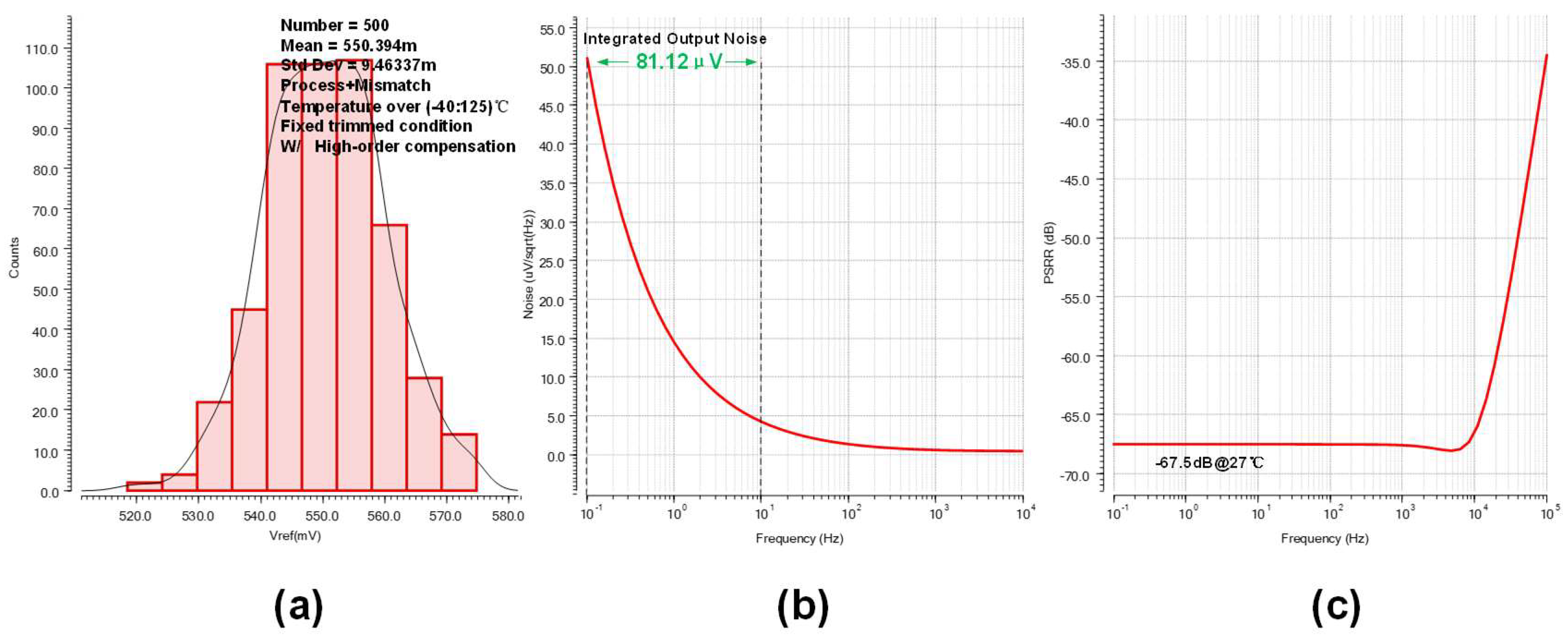
4.2. Simulation Results

Figure 8 shows the simulated temperature behavior of Vref at the TT process corner with varying supply voltage. It is observed that the proposed scheme successfully implements high-order temperature curvature compensation. In order to accurately evaluate the effect of process variation and power supply voltage on the circuit performance, the simulated TC results for different supply voltages and corners are summarized in Table 1. When the supply voltage is set to 1.3 V or 1.6 V under the SS process corner, Vref without high-order compensation is approximately a diagonal line. As a result, the TC with high-order compensation is larger than the TC values for other cases.
To assess the impact of process variation and device mismatch on the reference output Vref and TC, Monte Carlo simulations were completed using foundry-supplied statistical device models with activated mismatch and process variations. In order to observe the worst-case results, no specific correlation coefficients were defined for the matched devices. Figure 9a displays the estimated TC results without high-order compensation from 500 Monte Carlo runs under 1 V power supply voltage. Figure 9b shows the estimated TC results with high-order compensation from 500 Monte Carlo runs under 1 V power supply voltage. Comparing Figure 9a and Figure 9b, it is clear the normal distributions of TC are similar under fixed trimmed conditions. This is because high-order compensation is dependent on the outcome of first-order compensation. In certain process and mismatch conditions, the Vref will deviate significantly from the expected result. Therefore, trimming is necessary to ensure better measurement results.
Figure 10a displays the results of the estimated reference voltage Vref from 500 Monte Carlo runs under 1 V power supply voltage, indicating its stability. Figure 10b shows the noise spectrum of the simulated bandgap output under 1 V power supply voltage. The integrated output noise from 0.1 Hz to 10 Hz is 81.12 μV. The simulated PSRR of the BGR circuit under 1 V power supply voltage is shown in Figure 10c, where the PSRR at a low frequency is −67.5 dB at 27 °C.
In order to verify the effect of the trimming circuit, the results w/trimming and w/o trimming are shown in Figure 11a and used for a comparison. The estimated TC results w/trimming and TC results w/o trimming from 100 Monte Carlo runs under 1 V power supply voltage are presented in Figure 11a. The estimated TC results w/o trimming are in the range of 2 ppm/°C to 50 ppm/°C. The estimated TC results w/trimming are from 1.2 ppm/°C to 17 ppm/°C. The variance and mean of TC results w/trimming were improved to a great extent. This verifies the effectiveness of the trimming circuit. The Vref is mainly affected by the input-referred offset voltage within OPA in Figure 1. The temperature dependence of the input-referred offset is not modeled in this analysis, which assumes that the variation in temperature is small. Hence, the impacts on Vref can be captured with the following equations:
  I p = V e b + V O S R 0
I n = V e b + V O S R 1
  V r e f O S = V r e f + ( R 3 R 1 + R 3 R 0 ) V O S V r e f + 4.12 V O S
The σ of VOS are 1.5 mV, which is assessed based on the Monte Carlo simulations from 500 runs. Figure 11b displays the estimated Vref results w/trimming and Vref results w/o trimming. According to Equation (16), the σ of Vref affected by VOS is 6.18 mV. The estimated Vref results w/trimming and Vref results w/o trimming under 1 V power supply voltage presented in Figure 11b are essentially consistent. The variance and mean of Vref results are essentially the same. The σ of Vref is 9.5 mV, which is primarily affected by the VOS of OPA. This is generally consistent with the analysis. To reduce the systematic offset, a folded cascode amplifier with a gain greater than 60 dB is employed. To reduce the random offset, the sizes of transistors M14–M17 (the current mirrors in the OPA) and M19–M20 (the input pairs of the OPA) are enlarged. The extra methods, such as auto-zeroing and chopping techniques, are applied in the existing literature. These techniques are not used in this article because it is not the key point of this paper. Figure 12 shows the layout of the proposed BGR circuit implemented using a 0.18 μm Bipolar-CMOS-DMOS process. The performance summary and comparison of the proposed bandgap circuit is given in Table 2.

5. Conclusions

This proposed BGR with high-order temperature compensation was simulated using a 0.18 μm Bipolar-CMOS-DMOS process. The voltage difference of Veb at PTAT currents and ZTAT currents is used to generate a high-order compensation signal. The scheme presented in this work achieves a typical temperature coefficient of 1.2–15.5 ppm/°C from −40 °C to 125 °C. The probability of exceeding this TC range is about one percent, based on Monte Carlo simulations. Under 1 V supply voltage, it dissipates 36 μW power with an active area of 0.07986 mm2 at room temperature (27 °C). The integrated output noise from 0.1 Hz to 10 Hz is 81.1 μV. The PSRR at low frequency is −67.5 dB at 27 °C. The high-order temperature-segmented compensation BGR proposed in this work demonstrates superior stability and is well-suited for low-voltage and low-power applications.

Author Contributions

Conceptualization, S.J. and S.X.; methodology, S.J.; software, S.J.; formal analysis, S.J.; data curation, S.J.; writing—original draft preparation, S.J.; writing—review and editing, T.Y. and S.X. All authors have read and agreed to the published version of the manuscript.

Funding

This research received no external funding.

Data Availability Statement

Data are contained within the article.

Conflicts of Interest

The authors declare no conflicts of interest.

References

  1. Annema, A.J. Low-power bandgap references featuring DTMOSTs. IEEE J. Solid-State Circuits 1999, 34, 949–955. [Google Scholar] [CrossRef]
  2. Vulligaddala, V.B.; Adusumalli, R.; Singamala, S.; Srinivas, M.B. A Digitally Calibrated Bandgap Reference with 0.06% Error for Low-Side Current Sensing Application. IEEE J. Solid-State Circuits 2018, 53, 2951–2957. [Google Scholar] [CrossRef]
  3. Liu, L.; Liao, X.; Mu, J. A 3.6~μ Vrms Noise, 3 ppm/°C TC Bandgap Reference with Offset/Noise Suppression and Five-Piece Linear Compensation. IEEE Trans. Circuits Syst. I Regul. Pap. 2019, 66, 3786–3796. [Google Scholar] [CrossRef]
  4. Banba, H.; Shiga, H.; Umezawa, A.; Miyaba, T.; Tanzawa, T.; Atsumi, S.; Sakui, K. A CMOS bandgap reference circuit with sub-1-V operation. IEEE J. Solid-State Circuits 1999, 34, 670–674. [Google Scholar] [CrossRef]
  5. Ka Nang, L.; Mok, P.K.T. A sub-1-V 15-ppm/°C CMOS bandgap voltage reference without requiring low threshold voltage device. IEEE J. Solid-State Circuits 2002, 37, 526–530. [Google Scholar] [CrossRef]
  6. Huang, S.; Li, M.; Li, H.; Yin, P.; Shu, Z.; Bermak, A.; Tang, F. A Sub-1 ppm/°C Bandgap Voltage Reference with High-Order Temperature Compensation in 0.18-μm CMOS Process. IEEE Trans. Circuits Syst. I Regul. Pap. 2022, 69, 1408–1416. [Google Scholar] [CrossRef]
  7. Ma, B.; Yu, F. A Novel 1.2–V 4.5-ppm/°C Curvature-Compensated CMOS Bandgap Reference. IEEE Trans. Circuits Syst. I Regul. Pap. 2014, 61, 1026–1035. [Google Scholar] [CrossRef]
  8. Kamath, U.; Cullen, E.; Yu, T.; Jennings, J.; Wu, S.; Lim, P.; Farley, B.; Staszewski, R.B. A 1-V Bandgap Reference in 7-nm FinFET with a Programmable Temperature Coefficient and Inaccuracy of ±0.2% From −45 °C to 125 °C. IEEE J. Solid-State Circuits 2019, 54, 1830–1840. [Google Scholar] [CrossRef]
  9. Andreou, C.M.; Koudounas, S.; Georgiou, J. A Novel Wide-Temperature-Range, 3.9 ppm/°C CMOS Bandgap Reference Circuit. IEEE J. Solid-State Circuits 2012, 47, 574–581. [Google Scholar] [CrossRef]
  10. Yang, Y.; Binkley, D.M.; Li, L.; Gu, C.; Li, C. All-CMOS subbandgap reference circuit operating at low supply voltage. In Proceedings of the 2011 IEEE International Symposium of Circuits and Systems (ISCAS), Rio de Janeiro, Brazil, 15–18 May 2011; pp. 893–896. [Google Scholar]
  11. Yang, B.D. 250-mV Supply Subthreshold CMOS Voltage Reference Using a Low-Voltage Comparator and a Charge-Pump Circuit. IEEE Trans. Circuits Syst. II Express Briefs 2014, 61, 850–854. [Google Scholar] [CrossRef]
  12. Gagliardi, F.; Catania, A.; Ria, A.; Bruschi, P.; Piotto, M. A Compact All-MOSFETs PVT-compensated Current Reference with Untrimmed 0.88%-(σ/μ). In Proceedings of the 2023 18th Conference on Ph.D Research in Microelectronics and Electronics (PRIME), Valencia, Spain, 18–21 June 2023; pp. 61–64. [Google Scholar]
  13. Gagliardi, F.; Ria, A.; Piotto, M.; Bruschi, P. A 114 ppm/°C-TC 0.78%-(σ/μ) Current Reference with Minimum-Current-Search Calibration. IEEE Trans. Circuits Syst. II Express Briefs 2024, 71, 1561–1565. [Google Scholar] [CrossRef]
  14. Colombo, D.M.; Wirth, G.; Bampi, S. Sub-1 V band-gap based and MOS threshold-voltage based voltage references in 0.13 µm CMOS. Analog. Integr. Circuits Signal Process. 2015, 82, 25–37. [Google Scholar] [CrossRef]
  15. Ria, A.; Catania, A.; Bruschi, P.; Piotto, M. A Low-Power CMOS Bandgap Voltage Reference for Supply Voltages Down to 0.5 V. Electronics 2021, 10, 1901. [Google Scholar] [CrossRef]
  16. Gunawan, M.; Meijer, G.C.M.; Fonderie, J.; Huijsing, J.H. A curvature-corrected low-voltage bandgap reference. IEEE J. Solid-State Circuits 1993, 28, 667–670. [Google Scholar] [CrossRef]
  17. Tsividis, Y.P. Accurate analysis of temperature effects in Ic- VBE characteristics with application to bandgap reference sources. IEEE J. Solid-State Circuits 1980, 15, 1076–1084. [Google Scholar] [CrossRef]
  18. Tianlin, C.; Yan, H.; Xiaopeng, L.; Hao, L.; Lu, L.; Hao, Z. A 0.9-V high-PSRR bandgap with self-cascode current mirror. In Proceedings of the 2012 IEEE International Conference on Circuits and Systems (ICCAS), Kuala Lumpur, Malaysia, 3–4 October 2012; pp. 267–271. [Google Scholar]
  19. Ka Nang, L.; Mok, P.K.T.; Chi Yat, L. A 2-V 23-μA 5.3-ppm/°C curvature-compensated CMOS bandgap voltage reference. IEEE J. Solid-State Circuits 2003, 38, 561–564. [Google Scholar] [CrossRef]
  20. Osaki, Y.; Hirose, T.; Kuroki, N.; Numa, M. 1.2-V Supply, 100-nW, 1.09-V Bandgap and 0.7-V Supply, 52.5-nW, 0.55-V Subbandgap Reference Circuits for Nanowatt CMOS LSIs. IEEE J. Solid-State Circuits 2013, 48, 1530–1538. [Google Scholar] [CrossRef]
  21. Ji, Y.; Lee, J.; Kim, B.; Park, H.J.; Sim, J.Y. A 192-pW Voltage Reference Generating Bandgap– Vth with Process and Temperature Dependence Compensation. IEEE J. Solid-State Circuits 2019, 54, 3281–3291. [Google Scholar] [CrossRef]
  22. Malcovati, P.; Maloberti, F.; Fiocchi, C.; Pruzzi, M. Curvature-compensated BiCMOS bandgap with 1-V supply voltage. IEEE J. Solid-State Circuits 2001, 36, 1076–1081. [Google Scholar] [CrossRef]
  23. Chen, K.; Petruzzi, L.; Hulfachor, R.; Onabajo, M. A 1.16-V 5.8-to-13.5-ppm/°C Curvature-Compensated CMOS Bandgap Reference Circuit with a Shared Offset-Cancellation Method for Internal Amplifiers. IEEE J. Solid-State Circuits 2021, 56, 267–276. [Google Scholar] [CrossRef]
  24. Lovett, S.J.; Welten, M.; Mathewson, A.; Mason, B. Optimizing MOS transistor mismatch. IEEE J. Solid-State Circuits 1998, 33, 147–150. [Google Scholar] [CrossRef]
  25. Tan, M.; Liu, F.; Fei, X. A novel sub-1-V bandgap reference in 0.18 µm CMOS technology. In Proceedings of the 2011 IEEE International Conference on Anti-Counterfeiting, Security and Identification, Xiamen, China, 24–26 June 2011; pp. 180–183. [Google Scholar]
Figure 1. Traditional low-voltage BGR.
Electronics 13 01499 g001
Figure 2. Schematic of proposed low-voltage BGR with high-order compensation.
Electronics 13 01499 g002
Figure 3. (a) The curve of VebQ3, VebQ2 and Vref_1st with varying temperatures. (b) The curve of load current, IQ3, of Q3 and the compensation, Ic, with varying temperatures.
Electronics 13 01499 g003
Figure 4. Schematic of the OPA used.
Electronics 13 01499 g004
Figure 5. Start-up circuit.
Electronics 13 01499 g005
Figure 6. Simulated start-up waveforms of the proposed BGR.
Electronics 13 01499 g006
Figure 7. Trimming network of (W/L)M7.
Electronics 13 01499 g007
Figure 8. The simulated temperature behavior of Vref at TT process corner, with varying supply voltage.
Electronics 13 01499 g008
Figure 9. (a) The estimated TC results without high-order compensation from 500 Monte Carlo runs under 1 V power supply voltage. (b) The estimated TC results with high-order compensation from 500 Monte Carlo runs under 1 V power supply voltage.
Electronics 13 01499 g009
Figure 10. (a) The results of the estimated reference voltage output Vref from 500 Monte Carlo runs under 1 V power supply voltage. (b) The noise spectrum of the simulated bandgap output under 1 V power supply voltage. (c) The simulated PSRR of the BGR circuit under 1 V power supply voltage.
Electronics 13 01499 g010
Figure 11. (a) The estimated TC results w/trimming compared with TC results w/o trimming from 100 Monte Carlo runs under 1 V power supply voltage. (b) The estimated Vref results w/trimming compared with TC results w/o trimming from 100 Monte Carlo runs under 1 V power supply voltage.
Electronics 13 01499 g011
Figure 12. The layout of the proposed BGR with 0.18 μm Bipolar-CMOS-DMOS process.
Electronics 13 01499 g012
Table 1. The simulated TC results for different supply voltages and corners.
TC_bt (1 V)TC_at (1 V)TC_bt (1.3 V)TC_at (1.3 V)TC_bt (1.6 V)TC_at (1.6 V)
TT2.25 ppm/°C2.25 ppm/°C9.73 ppm/°C4.47 ppm/°C8.3 ppm/°C4.09 ppm/°C
FF14.3 ppm/°C5.61 ppm/°C15.87 ppm/°C6.69 ppm/°C12.96 ppm/°C6.21 ppm/°C
SS17.11 ppm/°C5.87 ppm/°C28.52 ppm/°C11.43 ppm/°C26.21 ppm/°C11.32 ppm/°C
TC_bt: The TC value before trimming. TC_at: The TC value after trimming.
Table 2. Performance summary and comparison of the proposed bandgap circuit.
ParameterThis Work *[7][9][22][23]
Technology0.18 μm0.18 μm0.35 μm0.35 μm130 nm
TypeCurrent-modeCurrent-modeCurrent-modeN/ACurrent-mode
Supply Voltage (V)11.22.51.0–1.83.3
Current Consumption (μA)363638N/A120
Reference Voltage (V)550 m767 m617.7 m692.6 m1.16
TC (ppm/°C)2.253.4–6.93.9255.8–13.5
Temperature Range (°C)−40–125−40–120−15–150−20–100−40–150
Active Area (mm2)0.079860.0360.10190.00450.08
PSRR (dB)−67.5 dB@DC−84 dB@DCN/A−55 dB@100−30 dB @100K
OUTPUT NOISE (V)81.1 μ (0.1–10 HZ)5.4 μ@320 Hz20 nV (0.1–50 HZ)26.8 μ (0.1–10 HZ)84.3 μ (0.1–10 HZ)
* Simulation results.
Disclaimer/Publisher’s Note: The statements, opinions and data contained in all publications are solely those of the individual author(s) and contributor(s) and not of MDPI and/or the editor(s). MDPI and/or the editor(s) disclaim responsibility for any injury to people or property resulting from any ideas, methods, instructions or products referred to in the content.

