1. Introduction
Demand for short-distance, high-speed wireless communication is increasing significantly for various applications, including chip-to-chip communication, intra-board communication, wireless ultra-high definition (UHD) transmission, etc. High-speed V-band On-Off-Keying (OOK) modulators significantly enhance wireless communication by enabling ultra-high-speed data transmission, making them suitable for integration into IEEE 802.11ad standard transceivers. These modulators facilitate faster, more reliable data exchange by minimizing signal distortion and boosting transmission efficiency, which is essential for bandwidth-intensive applications like high-definition video streaming and rapid data transfers within network infrastructures. This technology represents a critical advancement in meeting the growing demand for higher data throughput and reliability in wireless networks.
OOK modulation has the advantages of simple hardware architecture, small chip area, and low power consumption compared to more complicated modulation schemes such as quadrature amplitude modulation (QAM). Complicated signal processing like phase locking/recovery and frequency conversion are not required in OOK modulation as the amplitude of the carrier contains all the information. OOK is the preferred approach for creating a straightforward transceiver architecture that utilizes non-coherent modulation techniques. This method is acknowledged for its ease of use among the larger class of amplitude-shift keying techniques.
Two methods for transforming binary data into signals by shifting between ON and OFF states are categorized as active and passive OOK modulation. Each has advantages and disadvantages of its own. Transistors or other active devices are usually used in active OOK modulators, which are electronic components requiring external power for their operation. Conversely, passive OOK modulators employ passive components such as resistors, capacitors, and inductors for modulation, eliminating the need for external power and resulting in lower power consumption. This advantage is particularly significant in battery-powered or energy-sensitive applications, making passive modulators an ideal choice for enhancing energy efficiency in these circuits.
1.1. Related Work
Active-type OOK modulators can be implemented using different techniques like switching oscillator, modulating switch, switching amplifier, differential LO cancellation, etc. Switching oscillator-based OOK modulators [
1] directly control the oscillator with the data signal for modulation. This results in excellent on-off isolation as the oscillator stops producing output in the “off” state, eliminating unwanted signal leakage. However, when transmitting data at gigabit per second (Gbps) speeds, these modulators encounter a significant challenge due to the oscillator’s start-up time. Each time data signals switch from “off” to “on,” the oscillator requires a brief period to stabilize and produce the correct frequency. This start-up delay becomes a bottleneck at high data rates, limiting the system’s ability to process data efficiently. Overcoming this limitation in high-speed applications requires optimizing the oscillator design for quicker start-up times or adopting more sophisticated modulation techniques to ensure reliable data transmission without compromising modulation quality.
Modulating switches [
2] are appealing candidates for high-speed data transfer due to their fast-switching capabilities. High data rates are a vital component of contemporary communication systems. They must contend with conversion loss, which reduces signal power and negatively impacts the signal-to-noise ratio required for clear data transmission. Often, additional amplification stages are needed to reduce this loss and enhance the on-off ratio, which is vital for the clarity of digital signals. Even though these amplifiers help counteract the weaker signal, their complexity, higher power consumption, and potential for noise introduction complicate the system design. Despite these challenges, the fast switching speed of modulating switches and the ability to support efficient design make them indispensable for building complex communication networks. This implies that it’s essential to come up with creative ways to strike a balance between signal integrity, power efficiency, and speed.
In communication systems, switching amplifiers [
3] type OOK modulators are used for boosting signal intensity as they can obtain high conversion gains. They rely on swiftly changing the amplifier’s transistors from the on to the off state to amplify the input signal. However, they have low isolation, primarily due to signal leakage. The inadvertent occurrence of parasitic capacitance in transistors permits signal components to evade the amplification channel and it is a frequent source of this leakage. This type of signal leakage impairs the amplifier’s capacity to maintain clear, interference-free signal transmission, which is essential in high-fidelity communication applications. Sophisticated circuit design and material selection to reduce the parasitic effects are required to address this problem, ensuring that switching amplifiers maintain the high conversion gain and efficiency required in contemporary electronics.
The cancellation-based design [
4] offers three key benefits over the switch-controlled amplifier or oscillator approach. First, the continuous operation of the direct current (DC) path minimizes variations in bias current, thereby enhancing the speed of switching. Second, this design stabilizes the output impedance of the modulator, which supports the broadband performance of the transformer-matching network. Third, canceling out the radio frequency (RF) current negates the forward transmission caused by the parasitic capacitor, resulting in a better ON-OFF ratio. There are several approaches other than the one explained for the modulator design using the active approach.
Passive OOK modulators [
5] are mostly composed of passive components like CMOS switches. One distinct benefit is that they do not require DC power to function. This benefit results from the fact that passive OOK modulators are far more energy-efficient than active modulators as they do not have transistor DC bias currents, which is a feature of active modulators. However, when these modulators operate at higher frequencies, they face serious difficulties because of the parasitic effects that come with CMOS switches. The overall performance of the modulator degrades as a result of these effects, which include parasitic capacitances and resistances. It becomes more difficult to do high-speed modulation, which is essential for quick data transfer.
A crucial obstacle in the design of passive OOK modulators is managing the compromises imposed by the physical characteristics of CMOS switches. In particular, the gate width of the switching transistor is crucial. Expanding it might lower the on-state resistance and lessen insertion loss. It also increases parasitic capacitances, which may negatively affect modulation speed. On the other hand, narrowing the gate width increases on-state resistance but reduces parasitic capacitance, which may enhance the modulator’s efficiency by increasing its speed. This complexity draws attention to a basic limitation in the design of passive OOK modulators: the interdependence of CMOS switches’ on-state resistance and off-state capacitance prevents one from being improved without impacting the other. Although transistors with smaller length technology nodes could enhance data rate capabilities, this adjustment would result in higher manufacturing costs.
Using “distributed” or “travelling-wave” switches [
6] can relax such trade-off enabling high-speed operation up to several Gbps. In this technique, first, a single large switch is split into multiple smaller switches. Second, a series inductor is inserted for every small switch, forming an artificial transmission line with alternating series
L’s and shunt
C’s. The switch shunt capacitances, along with the series inductors, are then absorbed into the
LC transmission line, presenting a real impedance
at the switch input, up to the line cut-off frequency
. Modulation performance can be improved since the switch capacitance no longer forms an
RC pole, unlike a single large switch.
Several OOK modulators have been reported based on such distributed switches. In [
7], the drain line of cascaded FET switches was distributed for higher modulation bandwidth. In [
8], a similar approach was employed along with a gate-distributed line. A similar technique is implemented in [
9] with a transmission line in between the cascaded switches.
1.2. Our Approach
In this paper, we propose a 60 GHz distributed OOK modulator in 65 nm CMOS, where both the input and output lines are simultaneously distributed [
10]. The individual switch size and the number of stages were chosen considering overall OOK performance. On-wafer testing of the fabricated IC shows that the OOK modulator is fully functional with up to 5 Gbps of baseband signal (modulation bandwidth limited by the test setup). S-parameter testing shows <5 dB of insertion loss across 50 GHz–70 GHz, suggesting the proposed modulator has the potential for >5 Gbps operation.
2. Circuit Design
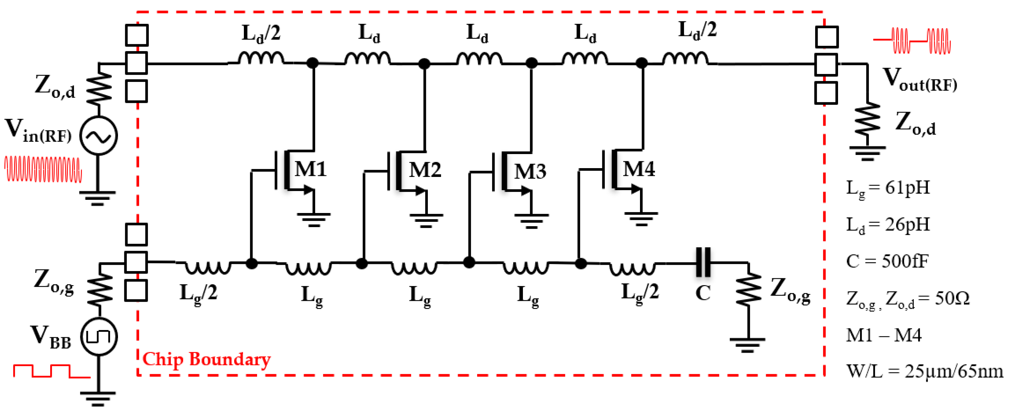
The schematic diagram of the proposed 60 GHz distributed OOK modulator in 65 nm CMOS is shown in
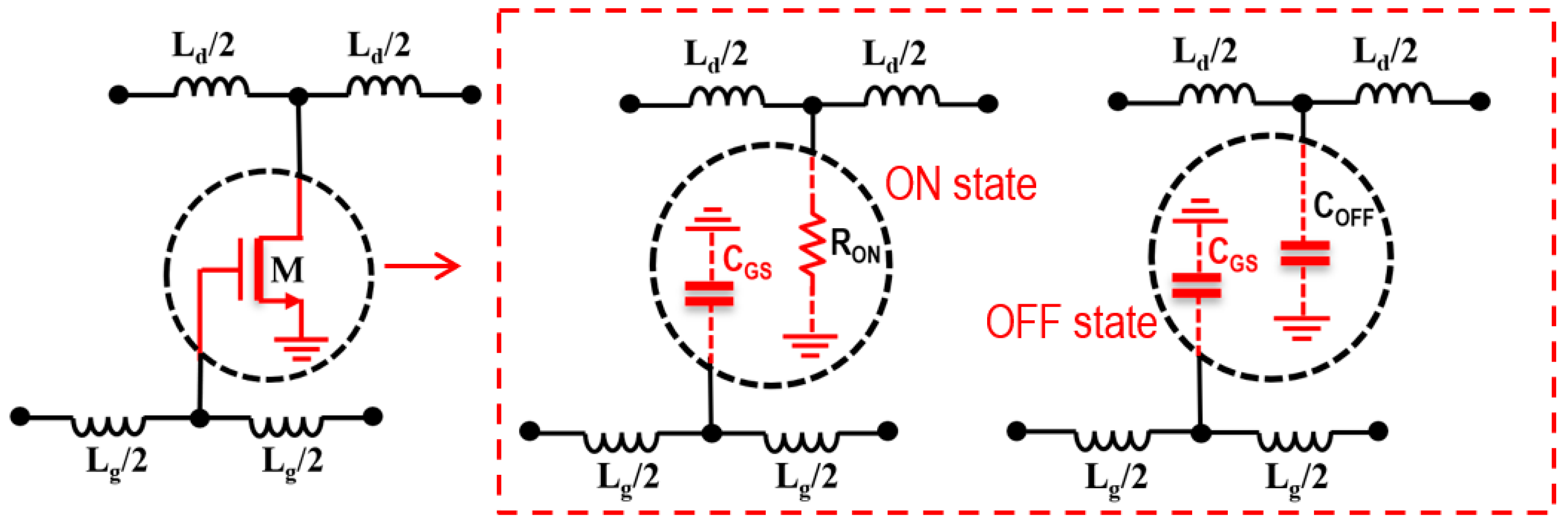
Figure 1. The design includes four transistors (M1–M4) working as single pole single through (SPST) CMOS switches. These switches are cascaded along with the two artificial transmission lines at the gate and drain terminals of each transistor to neutralize their respective gate and drain parasitic capacitances.
The baseband signal
VBB is applied at the input of the gate line, turning on or off all switches. The 60 GHz RF carrier signal
VIN(RF) is applied at the drain line input. When
VBB is high (“ON state” in
Figure 2), all transistors are turned on with a small on-state resistance
RON, isolating the RF signal from the output port
VOUT(RF). When
VBB is low (“OFF state” in
Figure 2), on the other hand, all switches are off with a shunt capacitance
COFF.
In OFF state, the switch capacitance COFF, along with drain inductors Ld’s, forms an artificial transmission line of , providing a low-loss signal path from VIN(RF) to VOUT(RF). Unlike a single non-distributed switch, it does not cause a significant attenuation from an RC pole. In a similar way, the switch input capacitance Cgs is absorbed into the artificial transmission line at the gate, along with gate inductors Lg’s, presenting a real impedance to the baseband signal VBB. The modulation bandwidth is thus enhanced due to the lack of an RC pole for a single, large switch. In short, using distributed lines at both the gate and drain allows for relatively low insertion loss and high modulation bandwidth.
There are performance trade-offs among the key design parameters: individual transistors width W and the number of stages N. For example, a larger W will reduce RON, improving the isolation at the ON state. However, it also increases COFF, which will, in turn, decrease the cut-off frequency fc for the same line impedance. The modulator will thus exhibit more insertion loss. Likewise, a smaller W will reduce the modulator insertion loss but at the expense of worse isolation. On the other hand, increasing N will both increase the modulator’s insertion loss and isolation, or vice versa.
One may choose
N for a reasonable compromise between the insertion loss and isolation. In this work,
N = 4 and
W = 25 μm were chosen, with COFF = 10.5 fF, Cgs = 24.7 fF, Ld = 26 pH, and
Lg = 61 pH. The gate and drain lines are thus matched to 50 Ω.
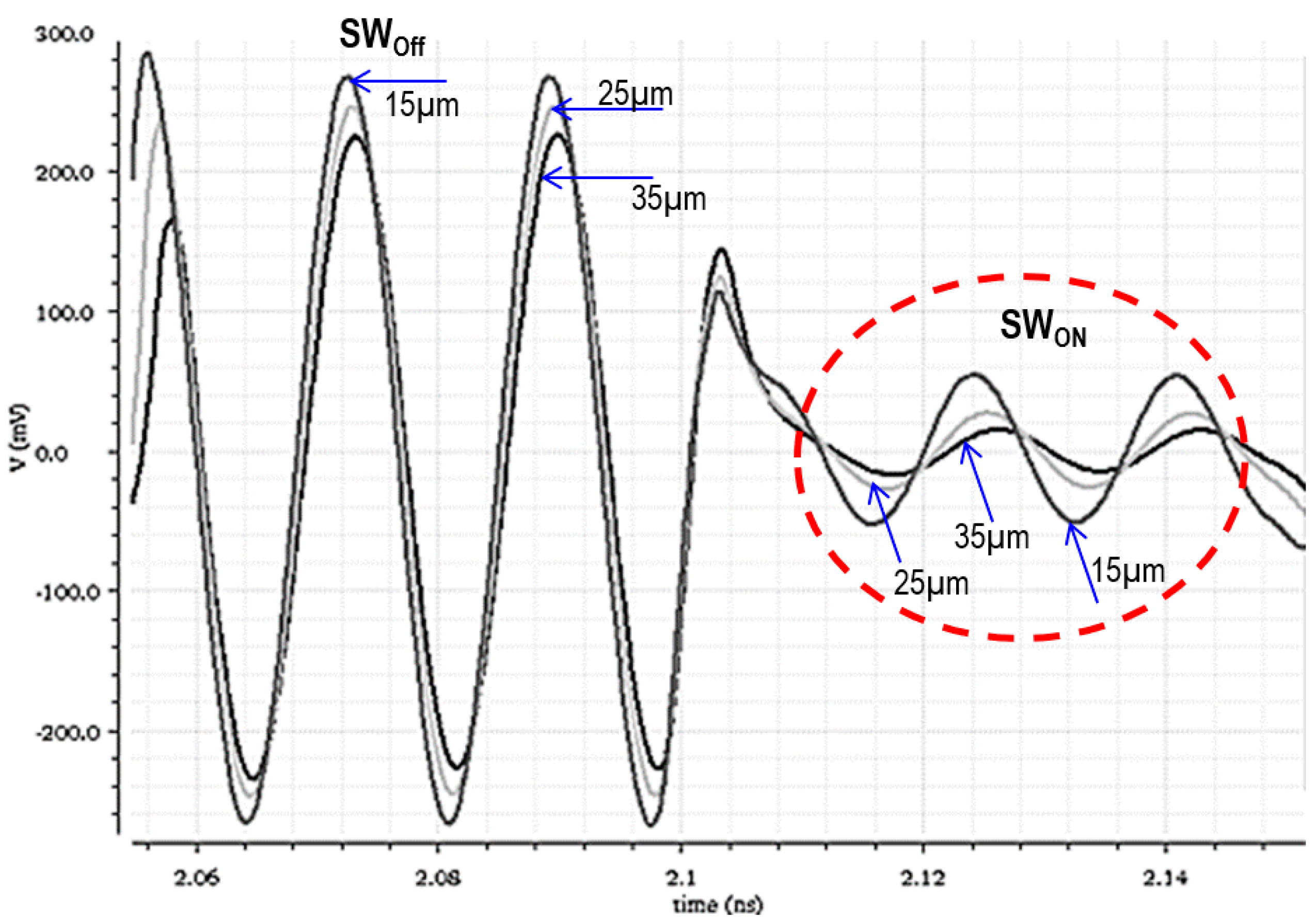
Figure 3 shows the simulation results of the modulator output at 60 GHz carrier with
W = 15 μm, 25 μm and 35 μm (
N = 4), where the effects of switch size
W on the modulator’s insertion loss (switch OFF) and isolation (switch ON) are clearly seen. The layout of the circuit has been crafted with meticulous attention to ensure that all stages are equidistant. Additionally, the extra traces linking the drain and gate sides of the transistor are designed as part of the inductor, thereby preserving the circuit’s optimized operational values.
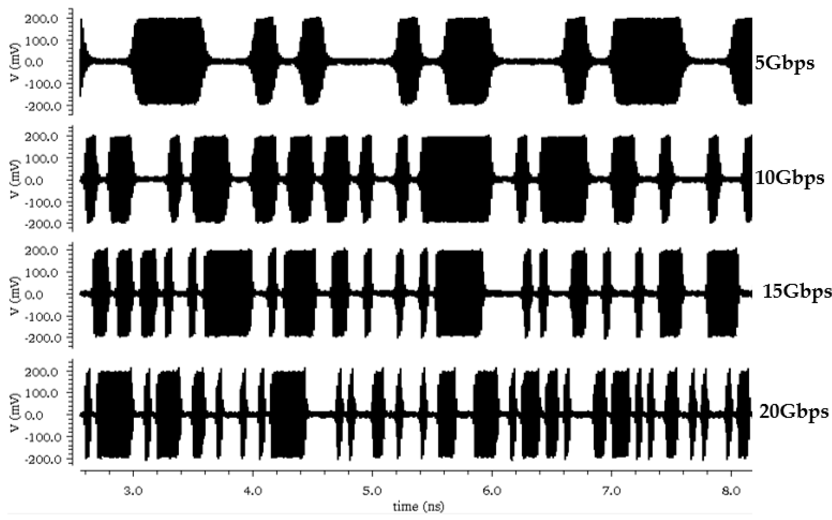
Finally,
Figure 4 shows the simulation results of the designed 60 GHz distributed OOK modulator with the baseband data rates up to 20 Gbps. All the layout parasitic and interconnects were modeled by EM simulation. The transient simulation results of the distributed OOK modulator exhibits clarity for both low and high baseband signals at speeds up to 20 Gbps. The Pseudo Random Bit Sequence (PRBS) sequence of 2
7–1 is used for all the time domain simulations of the proposed OOK modulator.
3. Measured Results
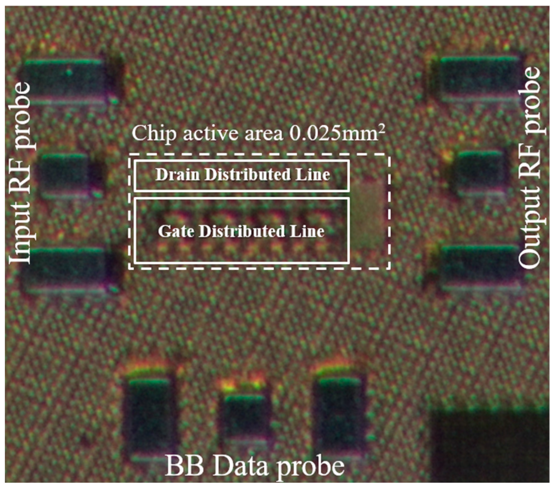
The designed V-band OOK modulator was fabricated using 65 nm CMOS technology. A microphotograph of the OOK modulator is shown in
Figure 5. The input RF pad is used to provide 60 GHz carrier signal to the fabricated chip and output RF pad is used to acquire the OOK–modulated output for further analysis.
The baseband signal to the modulator is provided through the baseband data pad. The chip operates without the need for DC biasing since the transistors activate or de-activate based on the baseband data state, eliminating the necessity of the DC pad on the chip. The area consumed by the distributed gate and drain lines is also highlighted in the chip photograph, which covers the major footprint of the fabricated chip. The overall chip size is 0.53 mm × 0.44 mm, including probing pads. The area of the core circuit part of the modulator is 260 μm × 96 μm.
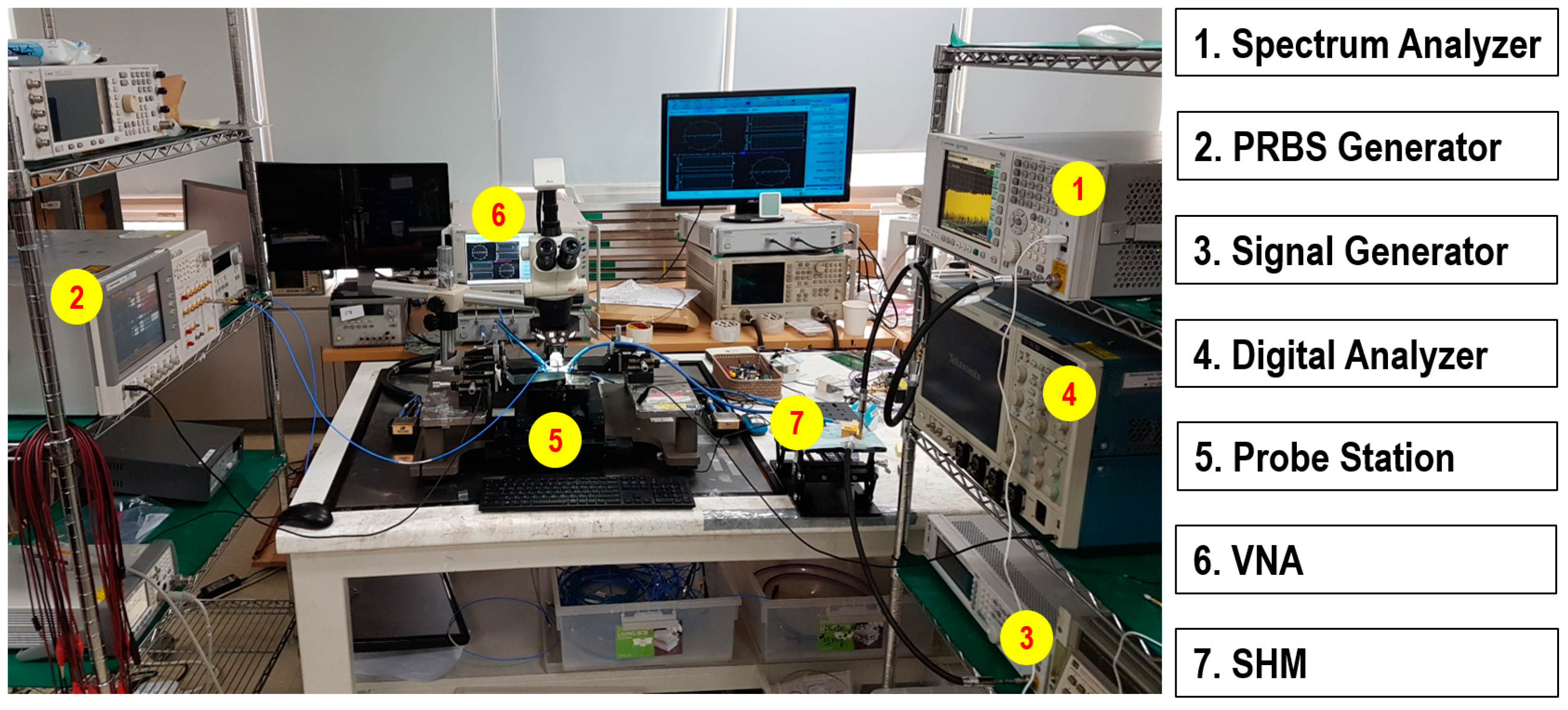
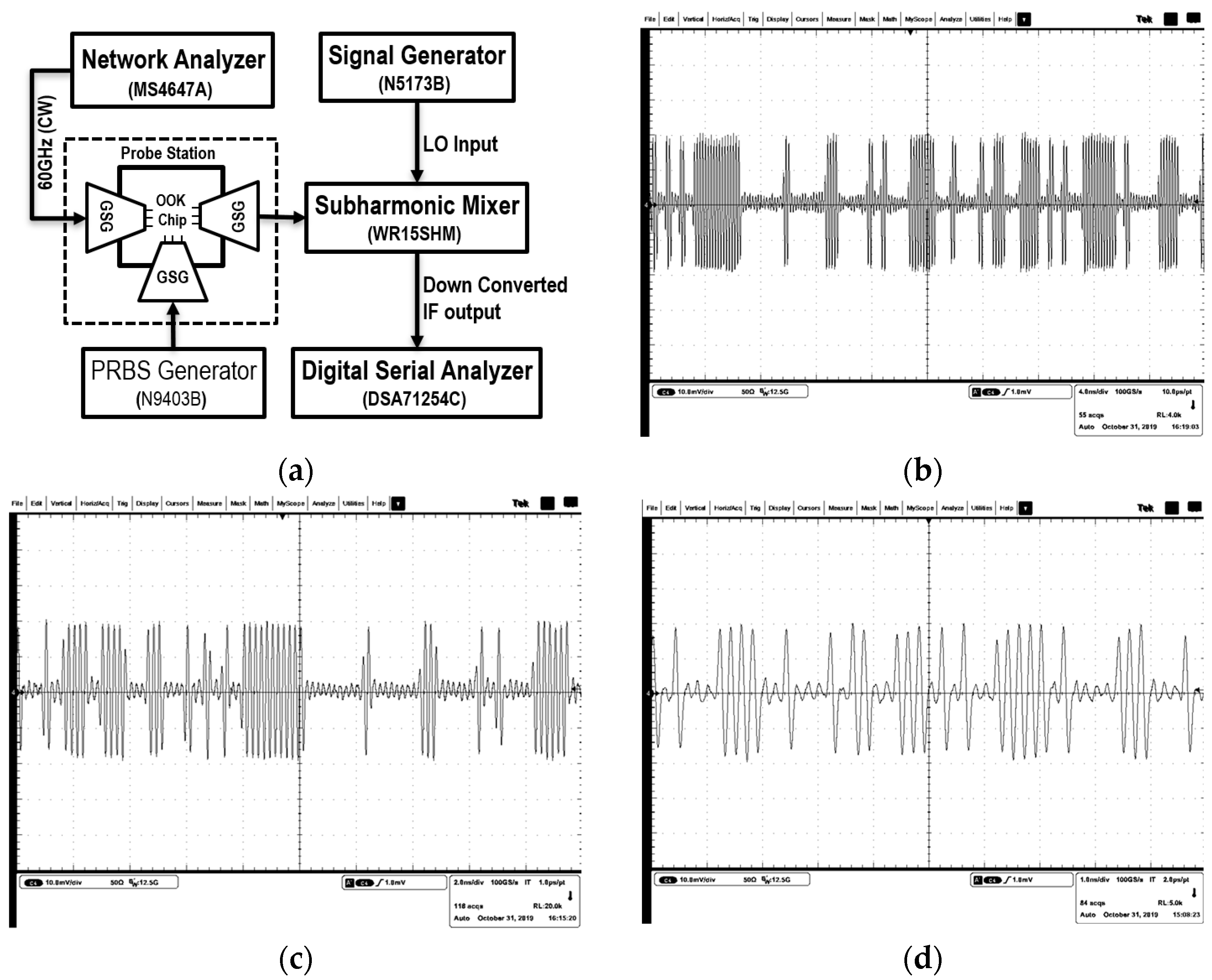
The fabricated IC was on-wafer tested using testing instruments shown in
Figure 6. An MS4647A vector network analyzer (VNA) from Anritsu was used for S-parameter measurement and for 60 GHz RF carrier generation. A J-BERT, N4903B from Agilent Technologies, was used to generate the baseband pseudo-random bit sequence (PRBS). For modulated time domain testing, the OOK modulator output was down-converted using a WR15SHM, V-band sub-harmonic mixer (SHM) from Virginia Diodes, whose sub-harmonic LO input was provided by N5173B from Keysight. The sub-harmonic mixer output was measured by either a DSA71254C digital signal analyzer from Tektronix or an N9030A spectrum analyzer from Agilent Technologies. The power supply E363121 from Keysight was required for S-parameter characterization, and the Cascade Microtech 9000 series probe system was utilized for all the measurements.
3.1. S-Parameter Measurements
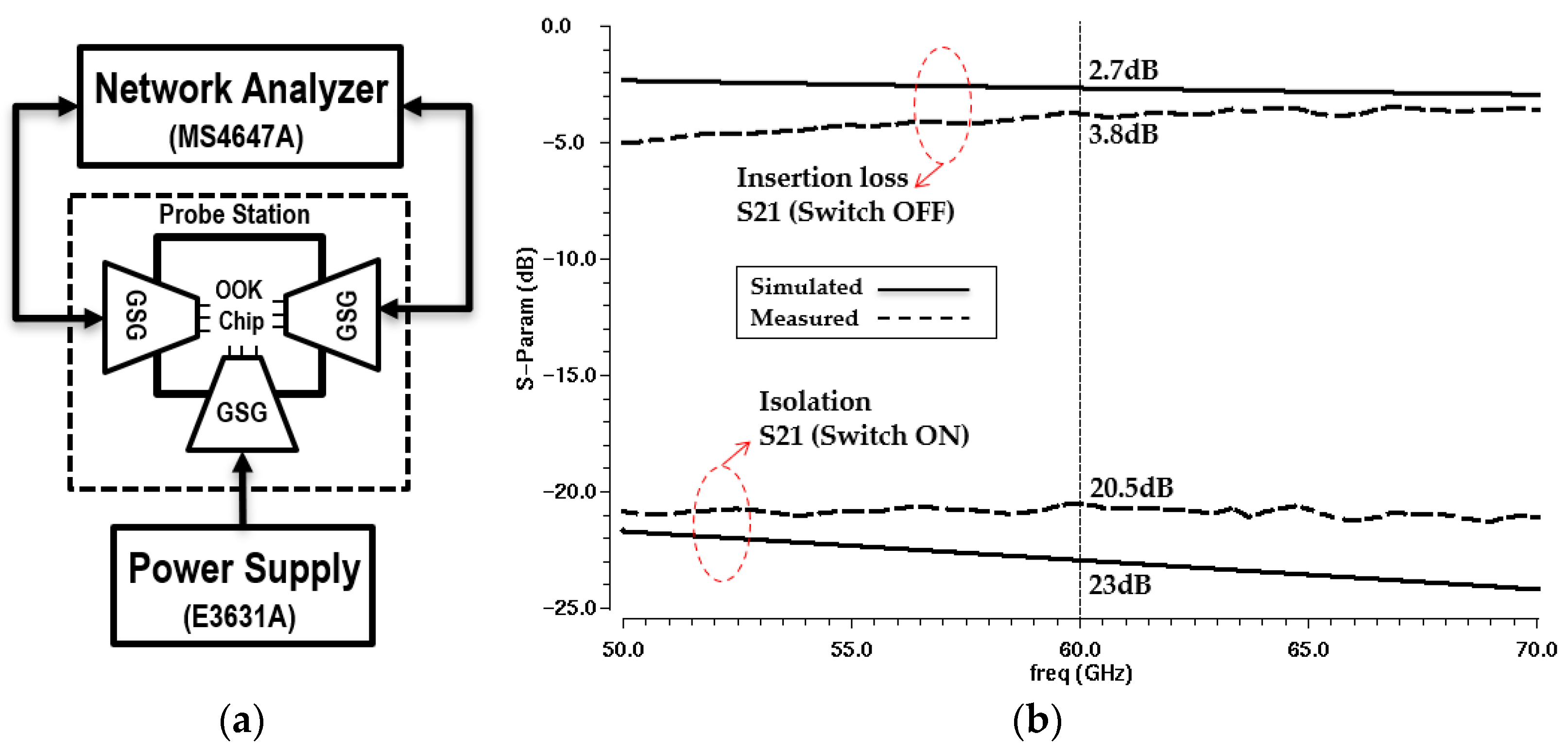
Test setup for S–parameter measurements is depicted in
Figure 7a. This setup requires a vector network analyzer MS4647A, a power supply E3631A and a probing station.
This setup is used to analyze the insertion loss and isolation of the fabricated modulator. The measured insertion loss and isolation of the OOK modulator are shown in
Figure 7b, along with the comparison of simulated results. The simulated insertion loss and isolation at 60 GHz are 2.7 dB and 23 dB, respectively, whereas the measured values of insertion loss and isolation are 3.8 dB and 20.5 dB, respectively. The discrepancy between simulation and measurement is attributed to modeling inaccuracies of layout parasitics as well as process variations. The measured on-off ratio of the modulator is greater than 16 dB from 50 GHz to 70 GHz. This depicts the reasonable difference in the ON-OFF ratio for a modulator to distinguish between high and low baseband data levels. The measured insertion loss is <5 dB from 50 GHz to 70 GHz, suggesting the fabricated OOK modulator is potentially capable of high-speed modulation beyond several Gbps.
3.2. Modulated Testing: IF Spectral Measurement
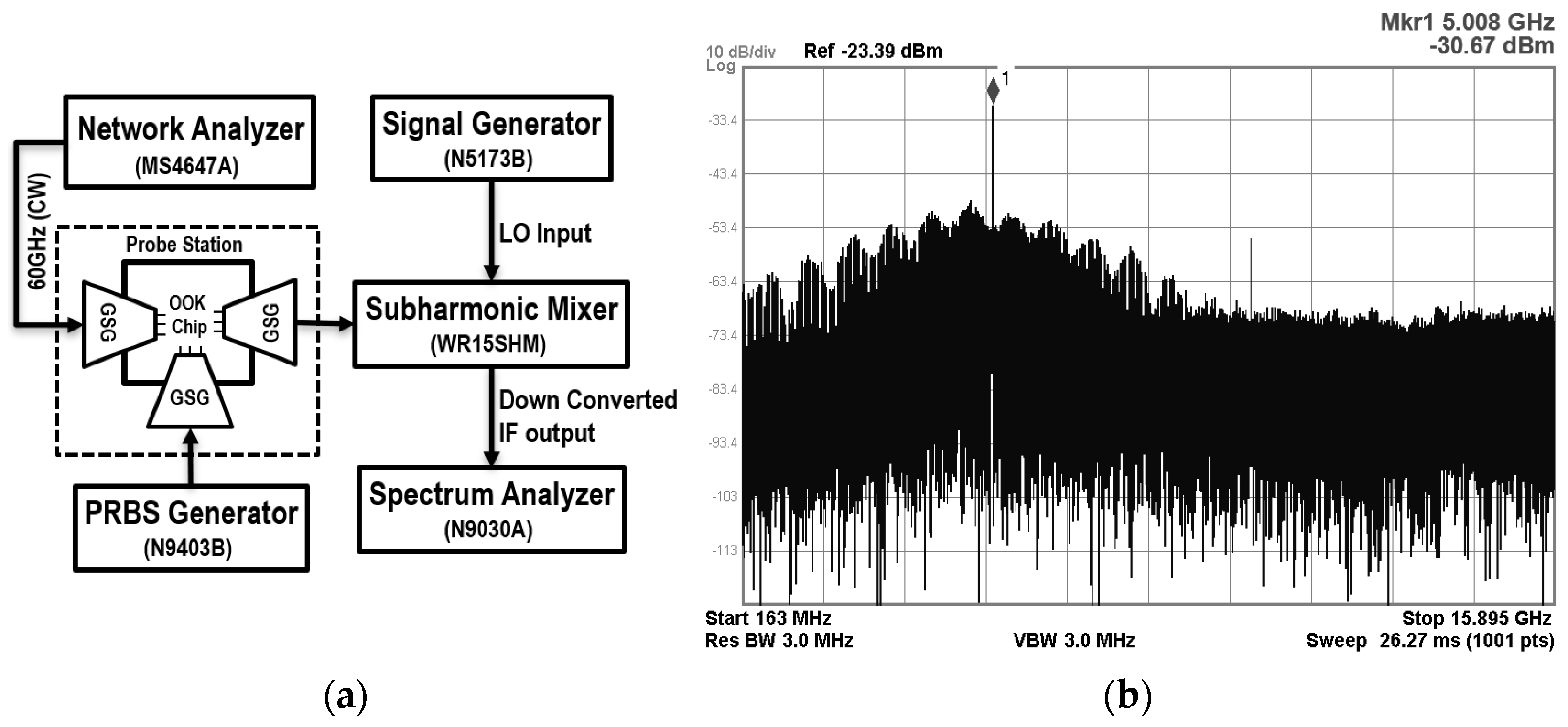
The setup shown in
Figure 8a is used to study the down-converted output spectrum of the fabricated modulator chip. It requires the vector network analyzer MS4647A for generation of the carrier signal, A PRBS generator N9403Band for generating baseband data of different rates, a sub-harmonic mixer (SHM) WR15SHM to down-convert the modulated output signal received from the fabricated chip. The SHM requires an LO signal that is applied through signal generator N5173B, and the IF output of the SHM is fed to Spectrum Analyzer N9030A for spectrum analysis. All these measurements were carried out on the Cascade Microtech 9000 series probe station.
The spectrum of the OOK modulator output with a 60 GHz carrier after down-conversion by the V-band sub-harmonic mixer is shown in
Figure 8b. The maximum IF frequency of WR15SHM is limited to 10 GHz, so the maximum possible baseband data rate is also limited to 5 Gbps with
fIF = 5 GHz. The IF spectrum closely follows the sinc(
x) function shape from dc to 10 GHz, including both sidebands. The 5 Gbps baseband input of the OOK modulator was driven by the PRBS generator N9403B (2
7-1).
3.3. Modulated Testing: IF Waveform Measurement at Different Data Rates
This setup is used to measure the time domain waveforms of the fabricated modulator chip. It requires the same measurement equipment as described in spectral measurement settings in last section despite that for analyzing time domain waveforms, the digital serial analyzer DSA71254C is used in place of spectrum analyzer. The measurement setup used for observing time domain waveform of the OOK modulator is shown in
Figure 9a.
After down-conversion to
fIF = 5 GHz, the mixer output was measured by a digital signal analyzer DSA71254C, as shown in
Figure 9b–d, at the rate of 2 Gbps, 3 Gbps and 5 Gbps, respectively. Similar to the spectrum measurement above, maximum data rate was limited to 5 Gbps due to the limited sub harmonic mixer’s IF bandwidth.
Table 1 compares recently published passive-type OOK modulators in CMOS for the frequency range of 60 GHz to 165 GHz. The proposed design underlies the switched modulators; therefore, it is compared with the other state-of-the-art modulators from the same category in CMOS technology. The presented work exhibits 8.3% of the normalized data rate (=data rate/carrier frequency), which is among one of the highest reported in the table.
The area of the core circuit, or active footprint, is 0.025 mm2, which is among one of the smallest footprints. Note that the modulated test setup in this work limits the maximum possible data rate to 5 Gbps. Relatively low measured S21 across 50 GHz to 70 GHz implies the presented OOK modulator can potentially operate at >5 Gbps. The bandwidth in [
12] is determined through single–tone testing by monitoring the strength of the modulated output signal in the frequency domain, and the modulator bandwidth is decided by a 3–dB drop point in the modulated signal magnitude plotted against the modulation frequency. The on–off ratio defined by the difference of isolation and insertion loss is 16.7 dB at 60 GHz and greater than 16 dB for the entire range from 50 GHz to 70 GHz for the proposed modulator, which is quite sufficient to translate the high and low values of the data bits. The designed modulator does not consume DC power.
4. Conclusions
In this paper, the design and measurement of a V–band CMOS OOK modulator based on distributed input and output transmission lines was presented. Small-signal and modulated testing reveals the proposed OOK modulator exhibits relatively high-speed operation with zero dc power consumption and a small die size, making it suitable for low-power high–speed communication systems.
Author Contributions
Circuit idea, M.S.; circuit design/layout, Z.M. and M.S.; on-wafer testing, Z.M.; writing—original draft preparation, Z.M.; writing—review and editing, Z.M. and M.S. All authors have read and agreed to the published version of the manuscript.
Funding
This work was supported by the Institute of Information & Communications Technology Planning & Evaluation (IITP) funded by the Korean Government (MSIT) through the Development of Key Technologies for 6G RF Front-End Based on Low-Power MIMO and Highly Efficient Spatial QAM Synthesis under Grant 2021-0-00198.
Data Availability Statement
The original contributions presented in the study are included in the article, further inquiries can be directed to the corresponding author.
Conflicts of Interest
The authors declare no conflicts of interest.
References
- Chang, H.-Y.; Lei, M.-F.; Lin, C.-S.; Cho, Y.-H.; Tsai, Z.-M.; Wang, H. A 46-GHz direct wide modulation bandwidth ASK modulator in 0.13-µm CMOS technology. IEEE Microw. Wirel. Components Lett. 2007, 17, 691–693. [Google Scholar] [CrossRef]
- Katayama, K.; Motoyoshi, M.; Takano, K.; Yang, L.C.; Fujishima, M. Fujishima. 209mW 11Gbps 130GHz CMOS transceiver for indoor wireless communication. In Proceedings of the 2013 IEEE Asian Solid-State Circuits Conference (A-SSCC), Singapore, 11–13 November 2013; pp. 409–412. [Google Scholar] [CrossRef]
- Byeon, C.W.; Eun, K.C.; Park, C.S. A 2.65-pJ/Bit 12.5-Gb/s 60-GHz OOK CMOS transmitter and receiver for proximity communications. IEEE Trans. Microw. Theory Tech. 2020, 68, 2902–2910. [Google Scholar] [CrossRef]
- Peng, Q.; Jia, H.; Fang, R.; Guan, P.; Deng, M.; Xue, J.; Deng, W.; Liang, X.; Chi, B. A 26-Gb/s 140-GHz OOK CMOS transmitter and receiver chipset for high-speed proximity wireless communication. In Proceedings of the 2023 IEEE Radio Frequency Integrated Circuits Symposium (RFIC), San Diego, CA, USA, 11–13 June 2023; pp. 145–148. [Google Scholar] [CrossRef]
- Zhou, T.; Dong, Y.; Gong, S.; Liang, S.; Ding, K.; Sun, X.; Gu, S.; Zhang, B.; Yang, Z.; Zhang, Y. A sub-terahertz high-speed traveling-wave switch modulator based on dynamically tunable double-resonant coupling units. IEEE Trans. Microw. Theory Tech. 2023, 71, 4346–4356. [Google Scholar] [CrossRef]
- Mizutani, H.; Takayama, Y. DC-110-GHz MMIC traveling-wave switch. IEEE Trans. Microw. Theory Tech. 2000, 48, 840–845. [Google Scholar] [CrossRef]
- Ye, Y.; Yu, B.; Gu, Q.J. A 165GHz OOK transmitter with 10.6% peak DC-to-RF efficiency in 65nm bulk CMOS. In Proceedings of the 2016 IEEE MTT-S International Microwave Symposium (IMS), San Francisco, CA, USA, 22–27 May 2016; pp. 1–4. [Google Scholar] [CrossRef]
- Hamada, H.; Kosugi, T.; Song, H.-J.; Yaita, M.; El Moutaouakil, A.; Matsuzaki, H.; Hirata, A. 300-GHz band 20-Gbps ASK transmitter module based on InP-HEMT MMICs. In Proceedings of the 2015 IEEE Compound Semiconductor Integrated Circuit Symposium (CSICS), New Orleans, LA, USA, 11–14 October 2015; pp. 1–4. [Google Scholar] [CrossRef]
- Suh, B.; Lee, H.; Kim, S.; Jeon, S. A D-Band Multiplier-Based OOK transceiver with supplementary transistor modeling in 65-nm bulk CMOS technology. IEEE Access 2019, 7, 7783–7793. [Google Scholar] [CrossRef]
- Oncu, A.; Takano, K.; Fujishima, M. 8Gbps CMOS ASK modulator for 60GHz wireless communication. In Proceedings of the 2008 IEEE Asian Solid-State Circuits Conference, Fukuoka, Japan, 3–5 November 2008; pp. 125–128. [Google Scholar] [CrossRef]
- Yamazaki, D.; Otsuki, Y.; Hara, T.; Khanh, N.N.M.; Iizuka, T. 11-Gb/s 140-GHz OOK modulator with 24.6 dB isolation utilizing cascaded switch and amplifier-based stages in 65-nm bulk CMOS. IET Circuits Devices Syst. 2020, 14, 322–326. [Google Scholar] [CrossRef]
- Kim, N.; Son, H.; Kim, D.-H.; Rieh, J.-S. A 130-GHz OOK transmitter in 65-nm CMOS technology. In Proceedings of the IEEE 16th Topical Meeting on Silicon Monolithic Integrated Circuits in RF Systems (SiRF), Austin, TX, USA, 24–27 January 2016; pp. 113–115. [Google Scholar] [CrossRef]
| Disclaimer/Publisher’s Note: The statements, opinions and data contained in all publications are solely those of the individual author(s) and contributor(s) and not of MDPI and/or the editor(s). MDPI and/or the editor(s) disclaim responsibility for any injury to people or property resulting from any ideas, methods, instructions or products referred to in the content. |
© 2024 by the authors. Licensee MDPI, Basel, Switzerland. This article is an open access article distributed under the terms and conditions of the Creative Commons Attribution (CC BY) license (https://creativecommons.org/licenses/by/4.0/).


