Article

A Large-Scale Neuromodulation System-on-Chip Integrating 128-Channel Neural Recording and 32-Channel Programmable Stimulation for Neuroscientific Applications

Department of Electronic Engineering, Pusan National University, Busan 46241, Republic of Korea
*
Author to whom correspondence should be addressed.
Electronics 2025, 14(20), 4057; https://doi.org/10.3390/electronics14204057
Submission received: 14 September 2025 / Revised: 12 October 2025 / Accepted: 13 October 2025 / Published: 15 October 2025
(This article belongs to the Section Bioelectronics)

Abstract

We present a large-scale neuromodulation system-on-chip (SoC) that integrates a 128-channel neural recording and 32-channel stimulation ASIC designed for a wide range of neuroscientific applications. Each recording channel achieves low-noise performance (~4 μVrms) with a configurable bandwidth of 0.05 Hz–7.5 kHz and supports 16-bit digitization with scalable sampling rates up to 30 kS/s. To enhance signal quality, the ASIC includes an adjustable digital high-pass filter and a fast-settling function for rapid recovery from stimulation artifacts. SoC also incorporates on-chip electrode-impedance measurements as a built-in safety feature by reusing the recording channels. The stimulation subsystem generates current-controlled monopolar biphasic pulses with a high compliance voltage of ±6 V using standard low-voltage (1.8 V/3.3 V) CMOS devices. Each of the 32 stimulation channels provides arbitrary 9-bit programmable waveforms and dual current modes (4 μA/bit and 8 μA/bit), supporting both fine-resolution microstimulation and high-current applications such as spinal-cord and deep-brain stimulation. On-chip charge-balancing switches in each channel further ensure safe and reliable stimulation delivery. The SoC supports digital communication via a standard SPI with both 3.3 V CMOS and low-voltage differential signaling options and integrates all required analog references and low-dropout regulators. The prototype was fabricated in a standard 180 nm CMOS process, occupying 31.92 mm2 (equivalently, 0.2 mm2 per recording-and-stimulation channel), and was fully validated through benchtop measurements and in vitro experiments.

1. Introduction

Understanding and modulating neural activity with high spatial and temporal resolution is a cornerstone of modern neuroscience and neuro-engineering. Advances in multichannel neural recording and stimulation technologies have enabled unprecedented insights into brain function, neural circuit dynamics, and the mechanisms underlying neurological disorders [1,2,3,4,5,6]. These technologies also underpin emerging therapeutic approaches, including deep brain stimulation (DBS), spinal cord stimulation (SCS), and brain–computer interfaces (BCI), which require precise, reliable, and scalable neural interfaces. However, as experimental and clinical demands grow, existing neural interface systems face several significant challenges. These include achieving simultaneous large-scale neural recording with low noise and high fidelity, providing programmable and temporally precise multichannel stimulations with safe charge balancing (CB), and integrating all functionalities into a compact, low-power, and scalable platform suitable for chronic implantation or portable use. Furthermore, the real-time monitoring of electrode–tissue interface conditions is essential to ensure long-term safety and stability yet is often overlooked or implemented externally. Recently, several neuromodulation system-on-chip (SoC) solutions have been introduced that integrate neural recording, stimulation, on-chip power management, safety mechanisms, and flexible communication protocols [1,2,3,4]. For example, a 64-channel neural recording and 2-channel time-multiplexed stimulation SoC with an integrated DC–DC converter and digital compression was presented in [1]. A 32-channel neuromodulation SoC capable of covering a wideband neural signal and delivering arbitrary high-voltage stimulation was demonstrated using commercial PtIr electrodes [2]. Furthermore, a BCI chipset supporting a 32-channel electrocorticogram (ECoG) recording and 4-channel stimulation was reported with a custom ECoG electrode in vitro [3]. A 128/8-channel, wireless neural interface based on custom neuromodulation SoCs and commercial off-the-shelf field-programmable gate array (FPGA) and radio modules was also demonstrated in combination with a commercial microelectrode array [4]. However, none of the previous works have achieved large-scale neural recording and concurrent multi-channel stimulation within a single monolithic chip. In [1], only two stimulation channels were implemented, limiting its applicability to experiments requiring parallel, multi-site stimulation. In [2], although a single-chip solution was demonstrated, the high-voltage stimulator circuits occupied a substantial portion of the ~25 mm2 die area, representing a fundamental bottleneck to scaling the channel count on a single die. Furthermore, other systems [3,4] adopted a two-chip architecture—a common practice in which low-noise recording front ends and high-voltage stimulation circuits are fabricated in separate, process-optimized dies. This multi-chip strategy, however, fundamentally constrains system miniaturization and increases packaging complexity. These issues are directly addressed in our single-chip integration using a standard CMOS process, which also provides a high compliance voltage. Among these prior works, only [2] incorporated an on-chip impedance-measurement feature to enhance safety. A detailed quantitative comparison of these systems is provided in the final section of this paper.
To address these challenges, we developed a neuromodulation SoC that integrates a 128-channel neural recording front-end and a 32-channel stimulation circuit within a single application-specific integrated circuit (ASIC). The recording channels are designed to capture the widest range of neural signals, from slow LFPs to high-frequency action potential (AP, or spike) activity with a reconfigurable bandwidth spanning 0.05 Hz to 10 kHz and providing a 16-bit digitization at scalable sampling rates up to 30 kS/s. The inclusion of an on-chip digital high-pass filter (HPF) and a fast-settling function allows for efficient artifact suppression and rapid signal recovery with <1 ms, which are critical for accurate neural data acquisition, especially during simultaneous stimulation. In addition, the SoC features integrated electrode impedance measurement (ZCHK) capabilities, spanning from 50 kΩ to 10 MΩ, allowing for the continuous monitoring of the electrode–tissue interface (ETI) to detect changes that may indicate degradation or failure, thereby enhancing device safety and reliability. The stimulation subsystem delivers current-controlled biphasic pulses with a high compliance voltage of ±6 V and output currents up to 2.048 mA. Each stimulation channel incorporates an independent 8-bit digital-to-analog converter (DAC) operating at up to 1 MS/s, enabling fully programmable waveforms with a minimum temporal resolution of 32 μs. Dual current modes—fine-resolution (4 μA/bit) and high-current (8 μA/bit)—support a broad spectrum of stimulation paradigms, from low-amplitude micro-stimulation to high-intensity therapies such as DBS and spinal cord stimulation. On-chip CB switches further ensure safe and effective stimulation delivery.
The SoC’s digital interface employs a standard serial peripheral interface (SPI) protocol with support for both 3.3 V CMOS input and output (I/O) and low-voltage differential signaling (LVDS), facilitating flexible integration with external control units. Additionally, the chip integrates all necessary analog reference generators and low-dropout regulators (LDOs), minimizing the need for external components and simplifying system design. Fabricated using a standard 180 nm CMOS process, the prototype SoC has undergone extensive characterization in benchtop setups as well as in vitro experiments, demonstrating robust performance and versatility across a wide variety of neuroscientific and neuromodulation applications. By integrating high-density, low-noise recording with flexible, high-compliance stimulation and built-in safety monitoring in a compact and power-efficient SoC, this work represents a significant step toward next-generation closed-loop neural interfaces and advanced bioelectronic therapies.

2. System Overview

This section describes the overall architecture of the proposed neuromodulation SoC. To accommodate the high channel count within a limited silicon area, a modular design and floorplan have been used.

2.1. Floor-Planning and Layout Overview

Figure 1a illustrates the physical layout and block allocation of the SoC. To support diverse applications, the SoC should offer flexible interfacing with neural probes through 128 recording and 32 stimulation pads, and the accommodation of >160 pads within the moderate size of the chip is challenging. For the interconnection, various bonding techniques, such as flip-chip, ball-bumping [5], and anisotropic conductive film (ACF) bonding [7,8], can be considered. If advanced flip-chip or anisotropic conductive film (ACF) bonding were employed, the footprint required for interconnection could be significantly reduced thanks to area-reuse bonding and the fine pitch (~20 µm for ACF, depending on the bump size) [7,8]. However, these methods require special post-processing and incur additional fabrication costs. Moreover, the ball-bumping process requires a dedicated pad area, which introduces similar geometric constraints to wire bonding when conventional bonding equipment is used, and it is effective only for very large chip sizes [4]. Therefore, in this work, standard wire bonding was selected for its compatibility and simplicity. Given the pad pitch limitations (~100–150 µm), a staggered pad arrangement with 90 µm pitch was adopted for recording inputs, enabling 128 input and 4 reference pads to be placed along the bottom edge of the chip. Accordingly, each recording channel (RPX) was assigned a width of 45 µm, resulting in a total die width of 5670 µm (128 × 45 µm). To manage layout complexity and provide local biasing, 32-channel recording modules were grouped, each sharing a reference circuit occupying the same width of 45 µm. Stimulation pixels (SPXs) are located at the top, spaced at 180 µm pitch, reflecting the 4:1 ratio of recording to stimulation channel numbers. Between the recording and stimulation blocks lies a digital interface comprising digital high-pass filters (D-HPF), SPI controllers, and register files, which control both subsystems and relay data externally. The power management unit (PMU), which supplies all required on-chip voltages, is centrally located. LVDS and 3.3 V CMOS I/Os are placed near the stimulation circuits to minimize interference with sensitive analog blocks. All critical blocks—including analog circuits and reference generators—are isolated using deep N-wells (DNWs) to suppress substrate noise and support the negative supply voltages (−6 V) required by the stimulators. The final chip size is 5940 µm × 3895 µm, comprising (i) a recording pixel: ~1050 µm height, (ii) an ADC and A-MUX: ~400 µm, (iii) a digital interface: ~750 µm, and (iv) a stimulation pixel: ~850 µm.

2.2. Overall Circuit Architecture

Figure 1b shows the block-level architecture of the SoC. Each RPX provides a bandpass filter (BPF)-shaped frequency response with a programmable mid-band gain (G), low- and high-pass cutoff frequencies (fL and fH); G is selectable among a fixed set of 200 and 400 V/V, and fH can also be chosen from 0.5, 0.85, 2, and 7.5 kHz, each coincides to the bands of LFP, Electrocorticogram (ECoG0, 1, respectively), and LFP + AP, respectively. Unlike it, fL is fixed as <0.5 Hz and is allowed to be tuned only if the fabricated chip results in a too-high or too-low fL. A 16-bit ADC is shared by each 32-channel module and digitizes signals using time-division multiplexing (TDM) via an analog multiplexer (A-MUX). The sampling rate is 30 kS/s per channel, sufficient for spike recording. The digitized data are filtered by a digital HPF, routed through an SPI, and transmitted via LVDS or CMOS drivers depending on user preference. Each SPX supports monopolar biphasic stimulation with independent control over anodic and cathodic amplitudes (IA and IC), pulse widths (tA, tC), and inter-phase delay (tD). The control timing resolution is defined by the SPI clock (25 MHz nominal), requiring 32 µs to update all 32 channels using 10-bit registers per stimulator. The stimulation current is programmable from 4 µA to 2.048 mA using on-chip 8-bit DACs. All parameters are configured via the SPI and shared digital interface. An integrated PMU includes seven LDOs and a low-voltage bandgap reference (BGR, 0.9 V), supporting internal voltages of 1.5 V, 1.8 V, 2.5 V, and ±3 V. The chip operates from a single 3.3 V supply (2.2–4.2 V range), with additional ±6 V supply for high-voltage stimulator operation.

3. Implementation

The detailed circuit implementation is described in this section, with conventional blocks omitted for clarity and brevity.

3.1. Recording Pixel (RPX)

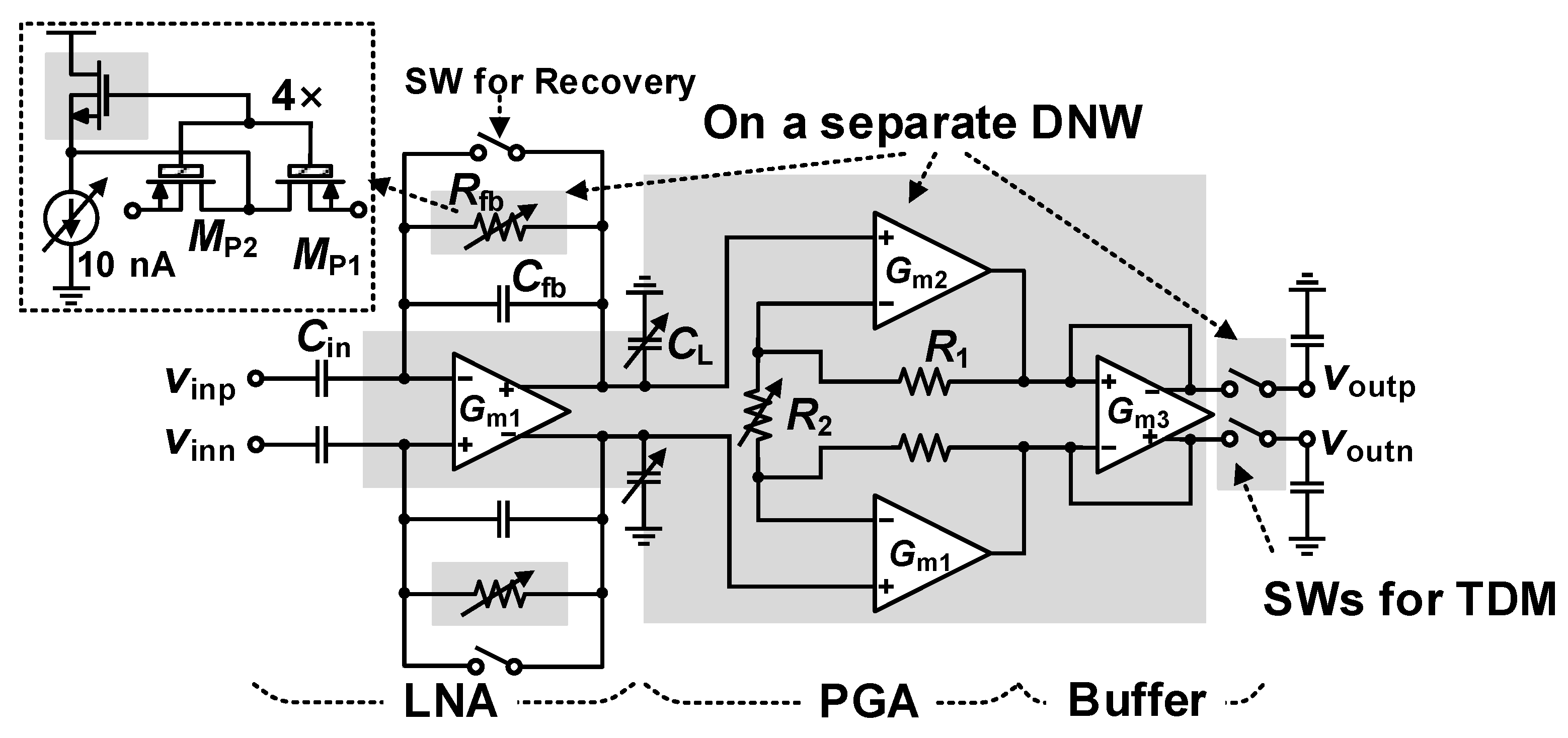
Figure 2 shows a circuit block diagram of a single channel RPX. It consists of a low noise amplifier (LNA), a programmable gain amplifier (PGA), and switches for TDM. Since the RPX is sensitive to interference, the entire signal processing circuits are physically isolated in a DNW from the TDM switches that generate switching noise. The TDM switches are also on a separate DNW. The LNA adopts a capacitively coupled architecture for high gain uniformity across channels and to avoid saturation due to electrode dc-offset drift [9]. Cin and Cf in the LNA are designed as 10 and 0.1 pF, respectively, to implement a nominal 40 dB of the mid-band gain. The fL and fH are primarily determined by the LNA. The fL, set by Rf and Cf, should be low enough (~0.1 Hz) to embrace slow-varying neural signals, such as LFP and ECoG, while rejecting the electrode dc-offset. Thus, Rf is implemented using four series-connected pseudo-resistors (PRs), as shown in Figure 2 [10], each comprises back-to-back, diode-connected high voltage (HV) PMOS transistors (MP1 and MP2), i.e., 3.3 V I/O transistors with a tunability using digital codes. In this work, 2-bit has been assigned with a nominal current of 10 nA, so that fL can be tuned from 0.01 to 1.5 Hz in simulation.
In addition, the AFE in neural recording interfaces is often designed to acquire band-limited neural signals such as LFP (~1 Hz–250 Hz), ECoG (~1 Hz–1~2 kHz), APs (300 Hz–7.5 kHz), etc. [9], thus it is necessary to control the fH of the LNA. In this work, the fH can be controlled using selectable output capacitance (CL) and varying transconductance of the LNA (Gm1) with 4 b code. The fH can be tuned from 0.5, 0.85, 2, and 7.5 kHz; thus, the LNA acts as an anti-aliasing filter to maintain the integrity of the neural signal and consumes only necessary power in accordance with the signal bands of interest. Additionally, to aid in rapid recovery from stimulation artifacts, a recovery switch is incorporated within the LNA. In the current implementation, this recovery switch is controlled manually via an SPI command. The 2nd-stage PGA has a standard instrumentation amplifier (IA) topology with resistive feedback, setting its gain to 1 + 2R2/R1. The unity-gain frequencies (ωT) of the operational amplifiers in this stage are also controlled by adjusting its bias currents, so the bandwidth can be programmed. The R1 and R2 in the PGA are set as 240 and 480 kΩ, respectively, at their nominal values to achieve a 6 dB gain; R2 can be programmable as 160 kΩ to increase overall gain G (200→400 V/V) using a switch [11]. The PGA is followed by a buffer to drive the switches used for the TDM. The maximum TDM rate is 1.024 MHz considering 32× multiplexing and 31.25 kS/s for each RPX. The switches are implemented using a separate triple well NMOS transistor to suppress artifacts from fast switching actions from degrading performance of the RPX. The entire circuit in a single RPX is laid out within 40 µm pitch and 5 µm (2.5 µm for the left and right) is used for physical separation between the channels to minimize crosstalk [12]. The RPX operates with a 1.5 V power supply and consumes ~36 µA of current.

3.1.1. Low-Noise Amplifier Design

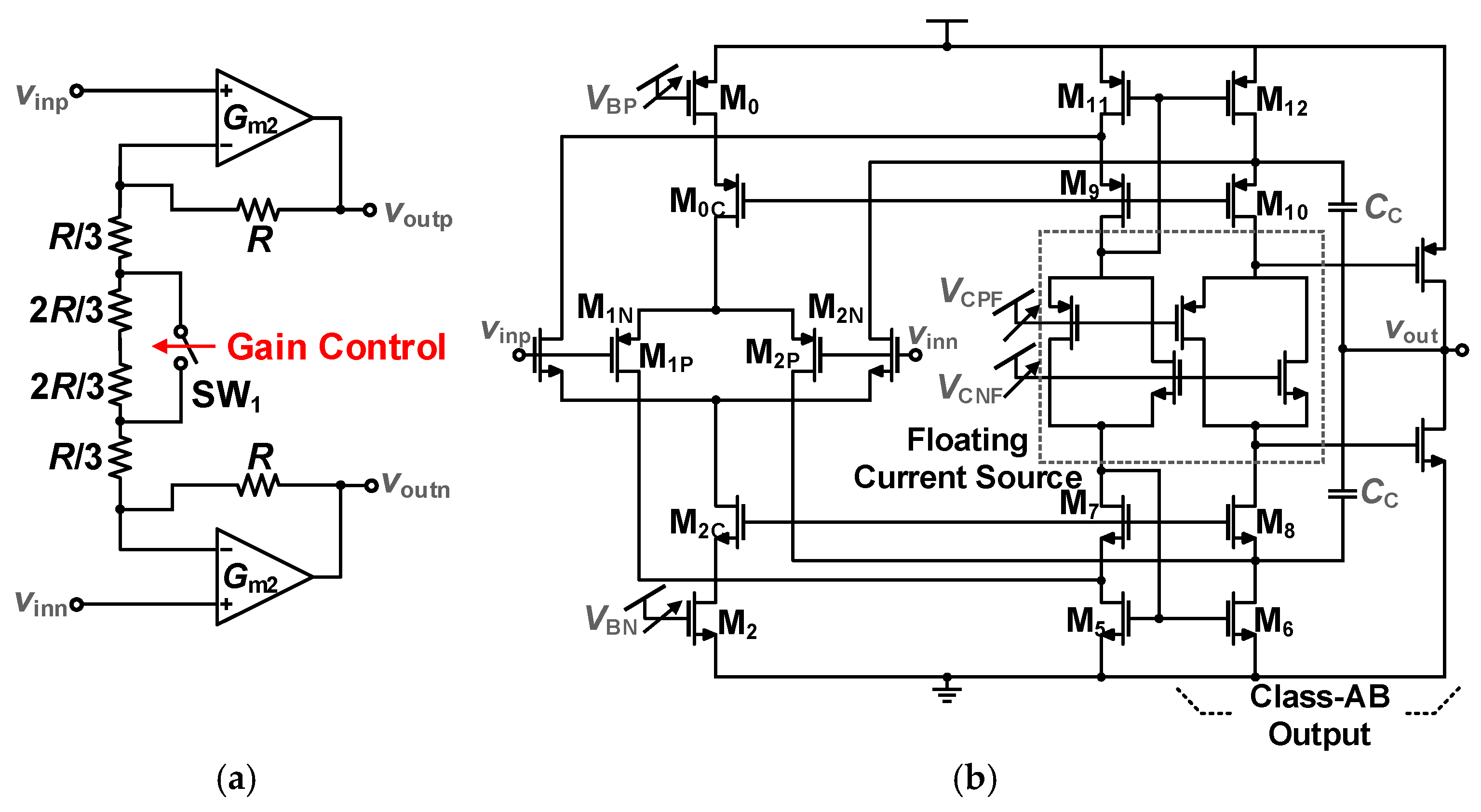
Figure 3a depicts transistor-level circuit diagram of the Gm1 for the LNA. Gm1 has been implemented using a two-stage operational transconductance amplifier (OTA) with local positive feedback (M5 and M6), and design principles of it for the LNA have been adopted from our previous implementation [13]. The spectral density of an input-referred noise (IRN) of the OTA, including thermal and flicker noises, is given by the following:
v - n , i n 2 8 k T γ 1 α 2 g m 1 + 2 K p W L C o x f
where gm1 is the transconductance of M1,2, γ is a constant for the transistor channel noise, k is Boltzmann constant, T is the absolute temperature, Kp is a process-dependent flicker noise coefficient, WL is the area of M1,2, and Cox is the gate oxide capacitance of M1,2. In addition, the value of Gm1 and ωT of the OTA are given by the following:
G m 1 = g m 1 B 1 α
ω T = G m 1 C L = g m 1 B 1 α C L
where gm1 is the transconductance of the input transistor, α and B are the ratios of (W/L)5,6/(W/L)4,3 and (W/L)10,9/(W/L)4,3, respectively, and CL is the load capacitance of the LNA. As shown, the advantage of the OTA is that the additional two design variables: α and B, separate the linear dependency of IRN and ωT (one is proportional, and the other is inversely proportional to Gm) on Gm in conventional OTAs. Thus, increasing gm1,2 and decreasing α (α < 1) can contribute to low noise performance, while the noise bandwidth (NBW) can be adjusted using B, instead of CL, which otherwise occupies large area. The overall noise of the LNA is determined by the product of a multiplication ratio (m, in Figure 3b) and IRN of the OTA, resulting in ~3 µVrms from 0.5 Hz to 50 kHz in simulations. As mentioned in the previous section, the fH of the LNA, which is given as (ωT/2π)∙(Cfb/Cin), is programmable using a 2 b digital code and adjustable bias current via VB1. The designed fH and IRN of the LNA for the 2 b code are as follows: (00): 9 kHz/2.64 μVrms, (01): 2.5 kHz/2.88 μVrms, (10): 1 kHz/3.00 μVrms, and (11): 0.5 kHz/3.07 μVrms, which can fully cover the AP, ECoG, and LFP bands. The LNA operates in fully differential manner. The LNA consumes 25 µA of bias current (including a bias network and the CMFB circuit) from a 1.5 V power supply.

3.1.2. Programmable Gain Amplifier and TDM Buffer Design

Figure 4 shows the block and transistor-level implementation of the PGA. It is implemented as an IA with DC-coupled resistive feedback to minimize gain variation by mismatch and achieve a high common-mode rejection ratio (CMRR). The PGA is controlled by a 1 b digital code, as shown in Figure 4a, so it can generate 6 or 12 dB gains. To ensure that the bandwidth of the RPX is unaffected by the different gains, the high frequency corner is designed to have >25 kHz at gain conditions of 12 dB. The OTA that configures the IA (Gm2) must satisfy the near output rail-to-rail condition and drive a resistive load (R), so a rail-to-rail input and output folded cascode (FC-OTA) with a class AB output topology has been adopted, and cascode Miller compensation (CC) was used to frequency-compensate Gm2 [14]. The bias of Gm2 can be adjusted by VBP and VBN, and the bias for the floating current sources for the class AB operation can also be adjusted by VCPF and VCNF.
A TDM buffer is needed to prevent linearity degradation of the previous block, such as the LNA and PGA, due to switching artifacts and settling time in TDM approaches. The TDM buffer is designed to maintain the linearity of the LNA and PGA, showing low distorting and meeting the near rail-to-rail input/output. Thus, a class AB unity gain buffer has been adopted [15]. The unity gain buffer is designed with a cutoff frequency of 20 MHz to ensure a stable settling time within 500 ns. The schematic of Gm3 is the same as Gm2 with the different aspect ratios for the constituent transistors.

3.2. Analog-to-Digital Converter

3.2.1. 16 b SAR ADC with Synchronous MSB and Asynchronous LSB Conversion

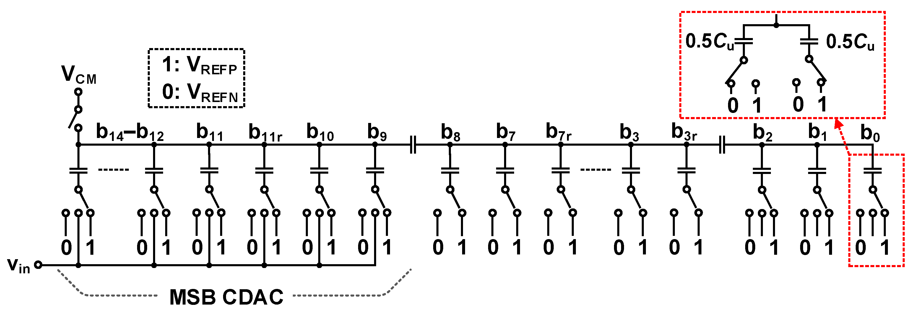
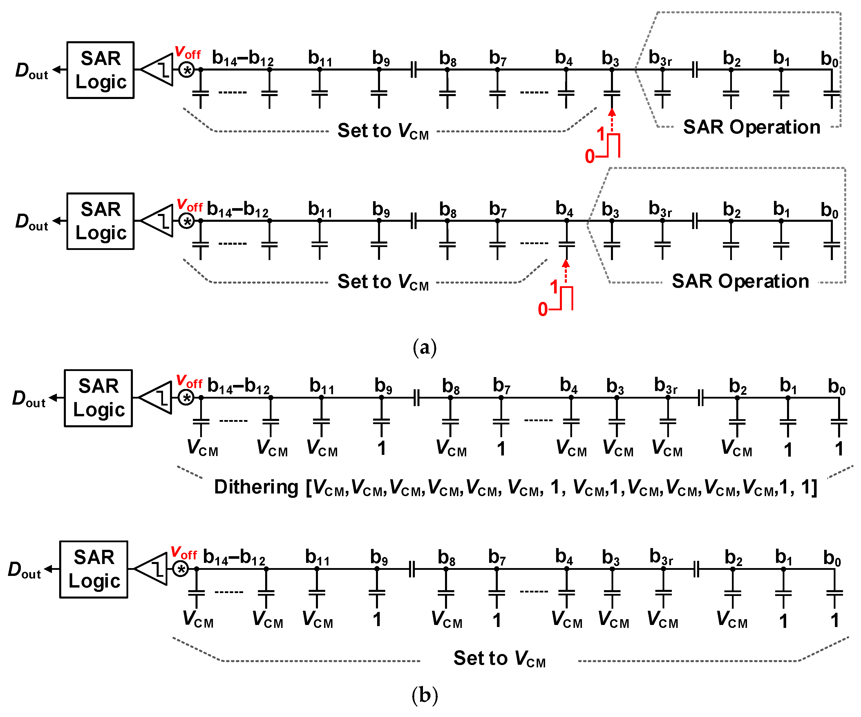
A 16-bit successive approximation register (SAR) analog-to-digital converter (ADC) is implemented for each 32-channel recording pixel (RPX) module. Figure 5 shows the capacitive digital-to-analog converter (CDAC) employed in the ADC, comprising three segmented capacitor arrays based on an 84 fF unit capacitor (CU). To enhance energy efficiency and maintain top-plate common-mode stability, a split-capacitor switching scheme is adopted. This approach eliminates the need for an additional bottom-plate reference voltage (VCM) for the ADC, as noted in [16]. The red-dotted box in the figure highlights the implementation of the CU based on this switching technique, with the switch positions configured for sampling at VCM. Since no dedicated bottom-plate VCM is used, a precise buffer is unnecessary. Instead, simple diode-connected transistors generate the top-plate VCM during sampling. The sampling capacitance is composed solely of the MSB segment of the CDAC (b14 to b9), with a total value of approximately 6 pF, which satisfies the required kT/C noise constraint (~26.27 µVrms). To accommodate incomplete charge settling during SAR conversion, three redundant bits (b11r, b7r, and b3r) are included. These redundant bits also serve as foreground calibration, as will be detailed later. Although the ADC is nominally designed to operate within 16 SPI clock (SCLK) cycles, 20 clocks are needed to account for the redundant bits. To support this, a hybrid control scheme is adopted: the first seven conversion steps—up to the bridge capacitor—are handled by synchronous logic to ensure adequate settling, while the remaining bits are processed asynchronously to improve speed and power efficiency [17].
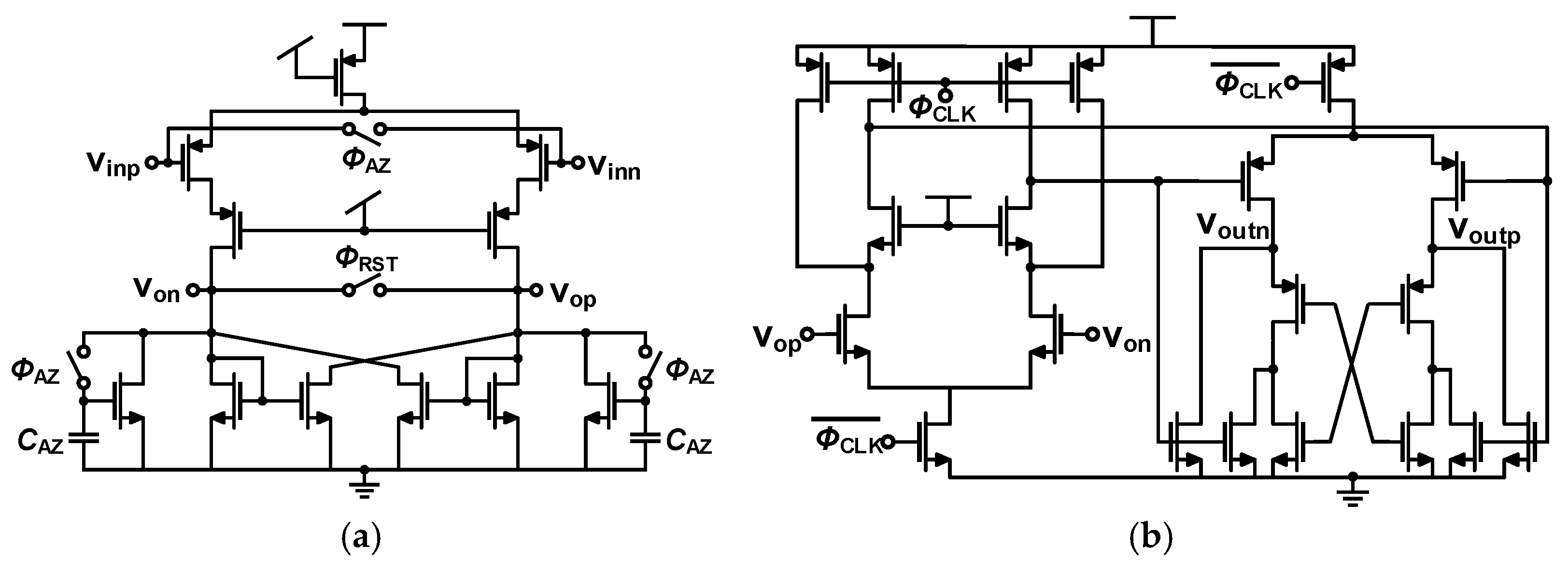
The comparator plays a critical role in determining ADC performance, particularly in balancing power consumption, noise sensitivity, operational speed, and architectural scalability. Figure 6 presents the transistor-level implementation of the comparator used in this work, which comprises a preamplifier stage followed by a dynamic latched comparator [18]. To suppress memory effects across successive conversions, the preamplifier is reset at the beginning of each comparison cycle via a ΦRST signal. The preamplifier operates as a differential integrator, and its load incorporates cross-coupled positive feedback to enhance DC gain and eliminate the need for a common-mode feedback (CMFB) circuit. The second stage consists of a single-phase dynamic latched comparator. Auto-zeroing (AZ) is also implemented at the preamplifier output; the AZ phase is aligned with the ADC sampling phase. During this phase, the inputs of the preamplifier are shorted and its offset is sampled onto the auto-zero capacitor (CAZ), effectively reducing systematic offset and 1/f noise. The overall comparator exhibits an estimated input-referred noise of approximately 140 μVrms, meeting the precision requirements of the 16-bit SAR ADC architecture. A single ADC consumes 740 μW where the buffer, preamplifier, comparators, logics, and DAC consume 470, 124, 38, 64, and 43 μW, respectively, and occupy 1.08 × 0.35 mm2.

3.2.2. Foreground Calibration

To correct bit weight errors caused by capacitor mismatch and parasitic, a foreground calibration is performed to improve linearity. Various SAR ADC calibration techniques have been proposed in the literature [19,20,21,22,23]. In this work, an on-chip foreground calibration method [21] with the split CDAC is proposed and implemented. The introduced split-CDAC not only eliminates the need for a dedicated reference generator (as discussed in the previous section) but also improves common-mode stability. In a typical CDAC, the lower-weight capacitors are less sensitive to mismatch due to their smaller bit weights [19]. Hence, as shown in Figure 7a (top), the capacitors corresponding to b0–b3r are assumed to be linear and are used to calibrate the higher-weighted capacitors (b3 in this case). During calibration, the target bit is toggled, and its weight is estimated by remaining bits into the digital domain using a partial SAR operation. The calibration is performed by toggling the bit under test between VREFP (=1) and VREFN (=0), while all higher bits are fixed at VCM. The lower bits are resolved by the SAR logic to estimate the digital output corresponding to the weight of the bit being calibrated. To eliminate the effect of offset during calibration, two weights: wi,force0 and wi,force1 are obtained by setting the target digital bit to 1, and 0, respectively, then, taking their difference yielding the calibrated bit weight is given by the following [21]:
w i = 1 2 ( w i , f o r c e 0   w i , f o r c e 1 )
w i , f o r c e 0 = j = 0 i 1 d j , f o r c e 0 w j + v o f f ,   w i , f o r c e 1 = j = 0 i 1 d j , f o r c e 1 w j + v o f f
where dj,force0 and dj,force1 are digital bits 0 and 1, respectively, and voff is the offset during the calibration. As a result, the extracted weight reflects only the true capacitor mismatch and is not affected by offset. This procedure is repeated sequentially for each bit up to the MSB, using the newly calibrated weights for the already corrected bits in the rest of Figure 7. Although the subtraction in (4) removes the offset ideally, this does not hold when the offset exceeds redundancy margin, resulting in saturation. To address this, during the sampling phase, the bottom plate of the capacitor under calibration is initially driven to 1 or 0 instead of VCM, and is subsequently returned to VCM, as shown in Figure 7b. This introduces a known offset proportional to the bit weight, which effectively shifts the calibration range and prevents output saturation. Since the same offset is introduced in both the “force 0” and “force 1” phases, it is canceled in the subtraction step in (4) and does not affect the linearity. Note that it is not necessary to apply a dither exactly equal to the circuit offset. Instead, a sufficiently large dither can be used to bring the signal within the valid calibration range, as illustrated in Figure 7b. This approach ensures robust calibration even in the presence of large offset.

3.3. Stimulation Pixel (SPX)

Neural stimulation typically uses a current-mode technique to inject a controlled charge into excitable tissue via electrodes [24]. Stimulation is delivered as biphasic current pulses (IA and IC), with adjustable phases (tA, tC, tD, and TC in Figure 1) for each current to ensure net-zero charge after stimulations. Stimulation currents typically range from tens of µA to a few mA, requiring voltage compliance from a few volts up to over 10 V due to varying ETI impedances. In this work, a high-compliance, fully on-chip neural monopolar stimulator is designed in a standard 1.8 V/3.3 V 0.18 µm CMOS process—avoiding HV CMOS. Custom circuit techniques ensure all devices’ voltage drops remain within their breakdown limits, enabling integration with other SoC components on a single chip.
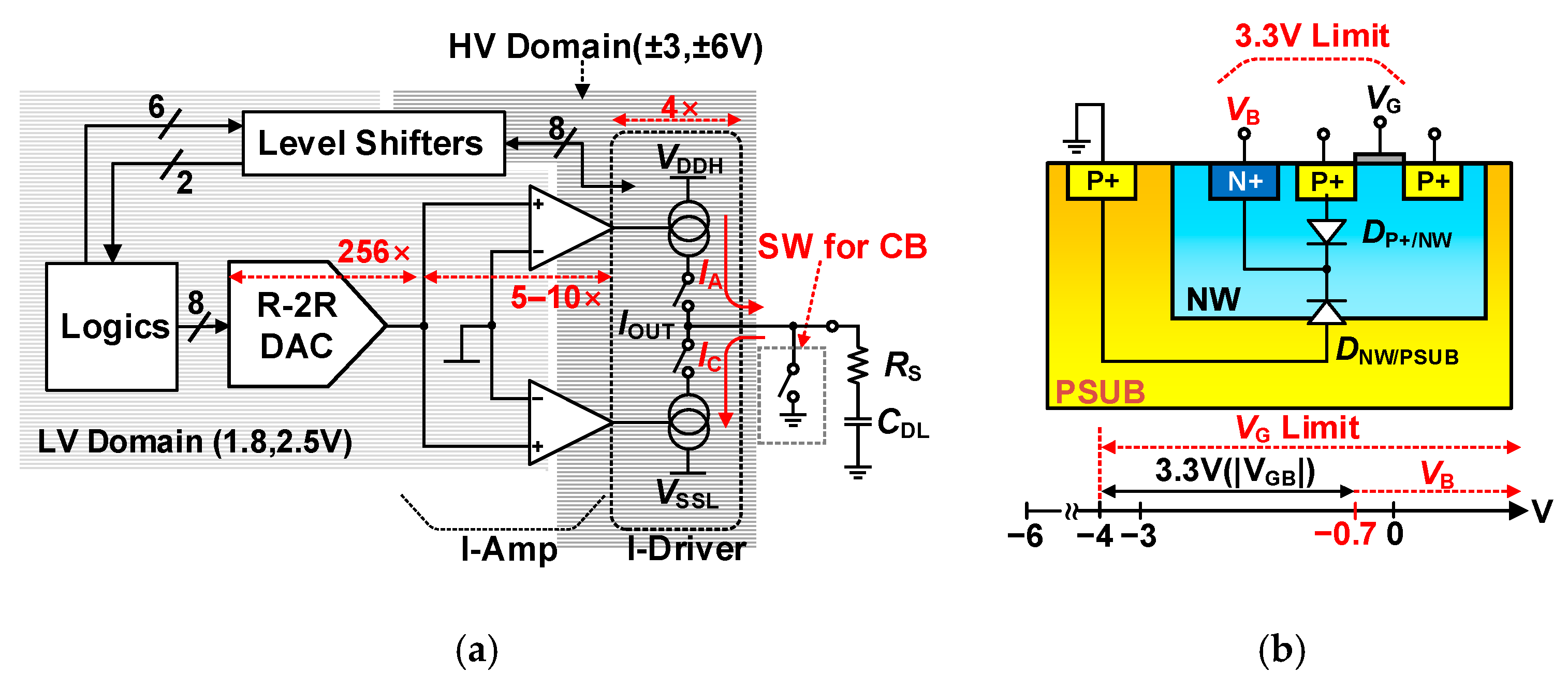
Figure 8a shows a single channel block diagram of SPX. Current mode stimulation is realized by a current driver (I-Driver) where balanced current sink and source are placed to provide IA and IC from 4 µA to 2.048 mA range with 9-bit resolution (8 b from DAC and 1 b for IA or IC selection). Covering the versatile applications of this neuromodulation SoC, in other words, the different ETI impedance ranges, for example: Cochlear [RS ≈ 4 kΩ, CDL ≈ 50 nF, 0.1–1.2 mA] [25], DBS [RS ≈ 1 kΩ, CDL ≈ 500 nF, 0.2–3.6 mA] [26], and muscle [RS ≈ 3 kΩ, CDL ≈ 20 nF, 0.2 mA] [27], the I-Driver has a compliance of ±6 V in consideration of its maximum current. The bias currents for the I-Driver are generated by a current amp (I-Amp) that scales 5–10× up of the current from 8 b DAC, which has the least significant bit (LSB) of 200 nA. As shown in the gray boxes in Figure 8a, The SPX requires both low voltages of 1.8 and 2.5 V, and high voltages ±6 and ±3 V, hence dedicated level shifters relay across those voltages. The level shifter not only delivers the timing information for IA and IC, but also does so for the compliance monitoring signals. Each SPX also has some combinational logic and flip-flops that decode the command from the SPI and deliver the violence of the compliance of the stimulator. The static current consumption of the SPX is ~167 μA.

3.3.1. Current Driver for Stimulation

This monopolar biphasic stimulation requires both positive and negative voltages. Thus, circuits operating with negative voltage must carefully handle parasitic p-n junctions, as the p-substrate (PSUB) in SoC integration must remain at 0 V to ensure compatibility across all blocks. Since the selected 180 nm CMOS process has DNW, all NMOS within the DNW can be placed regardless of polarity of the voltage rails if the junction voltages are within their breakdown voltages (BVs). However, a PMOS has difficulty being used between −6 and −3 V rail because a bias (VB) applied to the n-well (NW) of the PMOS must not be less than −0.7 V, otherwise a p-n junction diode between the PSUB and NW (DNW/PSUB) will be turned on, resulting in a significant leakage current or a gate oxide breakdown, as shown in Figure 8b.
According to the datasheet of the selected technology, the BVs of p-n junction diodes, DNW/PSUB and DP+/NW (P+−to−NW diode), are 14.8 and 10.3 V in their I/O transistors (3.3 V), respectively, and it means that a 3.3 V I/O PMOS and NMOS can sustain 14.8 V and −10.3 V, respectively, if the proper DNW bias for the NMOS is applied. However, we limited the supply rails within ±6 V in the current design to avoid too many transistor stackings and to ease design complexity, strictly imposed by the gate oxide BV limitation of 3.3 V.
Figure 9 illustrates a transistor-level schematic of a low side (LS) in the I-Driver to generate IC. The high-side (HS) of the I-Driver has the same configuration with different polarity of transistors. To sustain 6 V using 3.3 V I/O transistors (HVMOS: high-voltage MOS), multiple transistors are stacked, as shown in the configurations of M6L–8L and diode-connected transistors. The DNW for all diode-connected transistors are shared with the bias of the highest potential of 0 V in the LS circuit to minimize the area consumption. The I-Driver is basically a current mirror, copying a current from the I-AMP (M1L) and amplifying 4× (M1L) into the output of the driver (IOUT), turning on and off are governed by S0–2.
Note that the current mirror (M0L-M5L) is implemented using low-voltage transistors (LVMOS) for better matching, and it also uses a regulated cascode technique to control drain potentials (VDS) of M0L and M1L both to increase output resistance of the mirror and to improve matching (the red dotted box in Figure 9). The regulated cascode using amplifiers can suppress the voltage headroom of a current mirror [28], while improving matching of the current mirror by pinning VDS of the mirror transistors (M1) to VB∙A/(1 + A) with the aid of an amplifier (its gain is A), as shown in the gray dotted box in Figure 9; however, in this specific stimulator, PMOS transistors for the implementation of the amplifiers are unavailable in the VSSL to VDDL rails and implementing amplifiers are too much resource-consuming. Therefore, we implemented the regulated cascode using only two NMOS transistors (M4L and M5L) and bias currents. By applying proper bias currents, those are proportional to the output (or input) current, the VDS for M0L and M1L can be well matched because VGS in a transistor is proportional to a ratio of the drain current (ID) and aspect ratio (W/L) of the transistor (VGS ∝ √{ID/(W/L)}, assuming the all NMOS are deviated in the same direction under process, voltage, and temperature variations. The stimulator retains ~64% (16IB/25IB) of its current efficiency regardless of the magnitudes of IA and IC. The I-Driver also has a compliance monitoring function using a node information (VX), which can detect the triode region operation of M2L when the IOUT reaches ~−6 V. The voltage rise at VX is snatched by an inverter with hysteresis.

3.3.2. 8 b R-2R Digital-to-Analog Converter

To enable independent current control in each SPX, it must have a dedicated DAC. However, implementing a dedicated DAC per channel significantly increases chip area, posing a considerable integration challenge. Specifically, a conventional current-steering DAC structure, although its straightforward in operation, results in exponential transistor multiplication, consuming excessive chip area. Thus, an R-2R DAC architecture has been implemented to exploit its compact size compared to current-steering DACs. The resistance required for the R-2R DAC has been realized PMOS transistors (2.5 μm/2.2 μm) operating in their triode region [29]. The transistor’s on-resistance (Ron~1.1 MΩ) is leveraged as the resistive element, significantly shrinking the DAC’s physical footprint. The R-2R DAC can be laid out within 65.6 × 25.6 μm2. The implemented DAC has an LSB (least significant bit) of 200 nA, and it can generate currents up to a maximum of 51.2 µA (Ibias), offering the required precision and dynamic range.

3.3.3. Current Amplifier (I-Amp) and Level Shifters

The I-Amp is a set of current mirrors that copy the current from the R-2R DAC and deliver to the HS and LS of the I-Driver. The maximum gain of the I-Amp is 10× that is too large to copy in a single current mirror with a decent precision, thus it is segmented as 2.5× and 2× or 4× paths. For better matching between the HS and LS drivers, the regulated cascode used for the I-Driver has also been adopted in the I-Amp.
Since the SPX requires a different set of voltage rails, specific level shifters must be implemented. Figure 10a–c representatively shows some of the implemented level shifters from 1.8 V to VDDHVSSH, 1.8 V to VDDLVSSL, and VDDLVSSL to 1.8 V, respectively. Figure 10a,b can also be used for the shifting from 1.8 V to VSSHVCM and 1.8 to VCMVDDL, respectively, and a complimentary version of Figure 10c can also be used to realize a VDDHVSSH to 1.8 V conversion. Figure 10a is basically a level shifter with a cross-coupled pair, but with a modification of M1,2 to boost regeneration and also to provide voltage clamping of the node VX by the diodes (D1,2). Figure 10b is from [30] and the separation between the 1.8 V rail and negative rails are made from 5× series connected diodes that are realized by PMOS 3.3 V I/O transistors.

3.4. Digital Interface

The digital interface consists of SPIs to communicate with the external world and first order digital high-pass filters (HPFs) for each channel to remove offsets induced by the mismatch of the analog frontend and to provide an additional adjustment of fL according to users’ demands. The SPI inputs and outputs are transmitted to the CMOS or low-voltage differential signaling (LVDS) drivers.

3.4.1. SPI and LVDS

The implemented SoC integrates three dedicated SPI slaves—two for 128-channel neural recording and one for 32-channel stimulation. The control lines of the SPI (SCLK and CSB) are shared among three SPIs and two outputs: master-input-slave output (MISO) lines are for 128 channel recordings (each supports 64 channels at most) and one MISO is for 32 channel stimulations. The inputs: master-output-slave-input (MOSI) lines are also separately assigned for the recording (2×) and stimulation (1×). Each SPI period spans 950 ns, comprising 16 SCLK pulses with each of ~40 ns period and one CSB. A complete SPI cycle consists of 32 standard SPI periods and 3 auxiliary periods (35 × 950 ns), which roughly supports ~30 kS/s for each channel. For the case where this neuromodulation SoC has to drive a long-line (a few meters) in a headstage [5], it integrates LVDS transmitters (TXs) and receivers (RXs) on the chip. The specifications of the LVDS RX and TX follow the industrial standard for compatibility with any commercial SPI masters. Since the standard LVDS waveforms have a specified amplitude (~350 mV) with a designated end-line resistance of 100 Ω, the LVDS TX consumes ~4 mA current that is not appropriate for some biomedical applications. Therefore, the RX and TX are turned-on/off according to the users’ settings and the communication can be replaced by standard 3.3 V I/O.

3.4.2. Digital High-Pass Filter

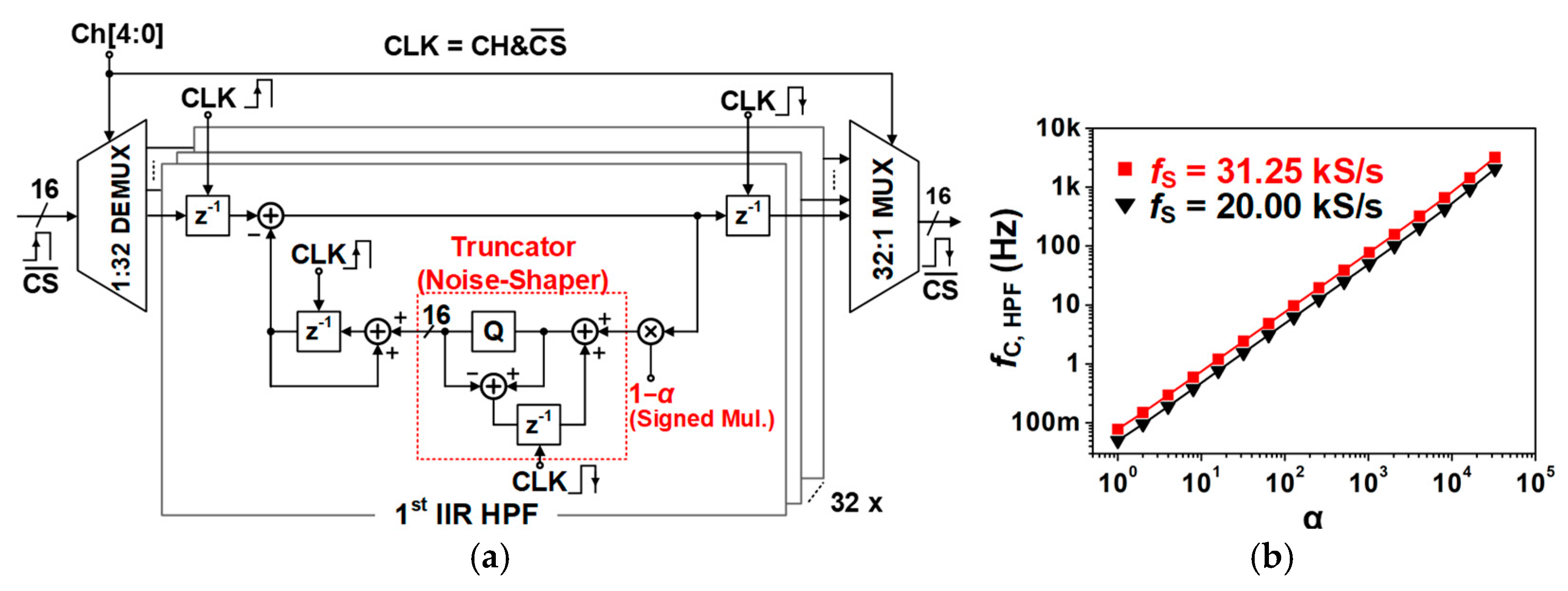
The block diagram of 32× infinite impulse response (IIR) D-HPFs is shown in Figure 11a. A total of 4× of them have been implemented. The HPF synchronously operates with the rising and falling edge of C S ¯ signal and channel information (Ch [4:0]). The z-domain which transfers function of the D-HPF is as follows:
H z = 1 z 1 1 α z 1
where α is a real pole and 0 < α < 1. The filter uses a first-order noise shaper (truncator) to reduce the truncation error due to the fixed-point error of the leaky integrator by the term, α [31]. Instead of the conventional cascade structure of a differentiator and a leaky integrator, this D-HPF realizes a single loop with a digital integrator in loop feedback. Due to single loop feedback without differentiator, no additional bit-extension for subtraction is required for 16 b data processing, resulting in area-efficient data processing with a 16 b bit-length. Also, to efficiently reduce this area, the 16 b multiplication logic is removed, and the D-HPF is configured to arithmetic shift logic for multiplication by two. This results in a dramatic ~70% reduction in the D-HPF to ~10,000 μm2/Ch. (~24,000 μm2 for a 16 b multiplication logic). As a result, the area consumption of the D-HPF per channel is ~32,000 μm2 which contributes to the huge area of the on-chip DSP. Figure 11b shows the variable cutoff frequency (fC,HPF) of the D-HPF vs. α. For fS = 20 kS/s and 31.25 kS/s, fC,HPF = 0.04992 and 0.078 Hz can be realized with the minimum α, which acts as a nearly perfect DC-blocker, while fC,HPF = 2.048 and 3.2 kHz with the maximum α, respectively. The α is tunable with a 4-bit code.

3.5. Impedance Measurement

Over time, biological tissue responses can alter the ETI, impacting both the electrode and the quality of recorded neural signals, thus continuous monitoring of the ETI (ZE) is essential to ensure long-term safety. Moreover, ZE measurement before and after system assembly can improve yield by identifying defective electrodes.
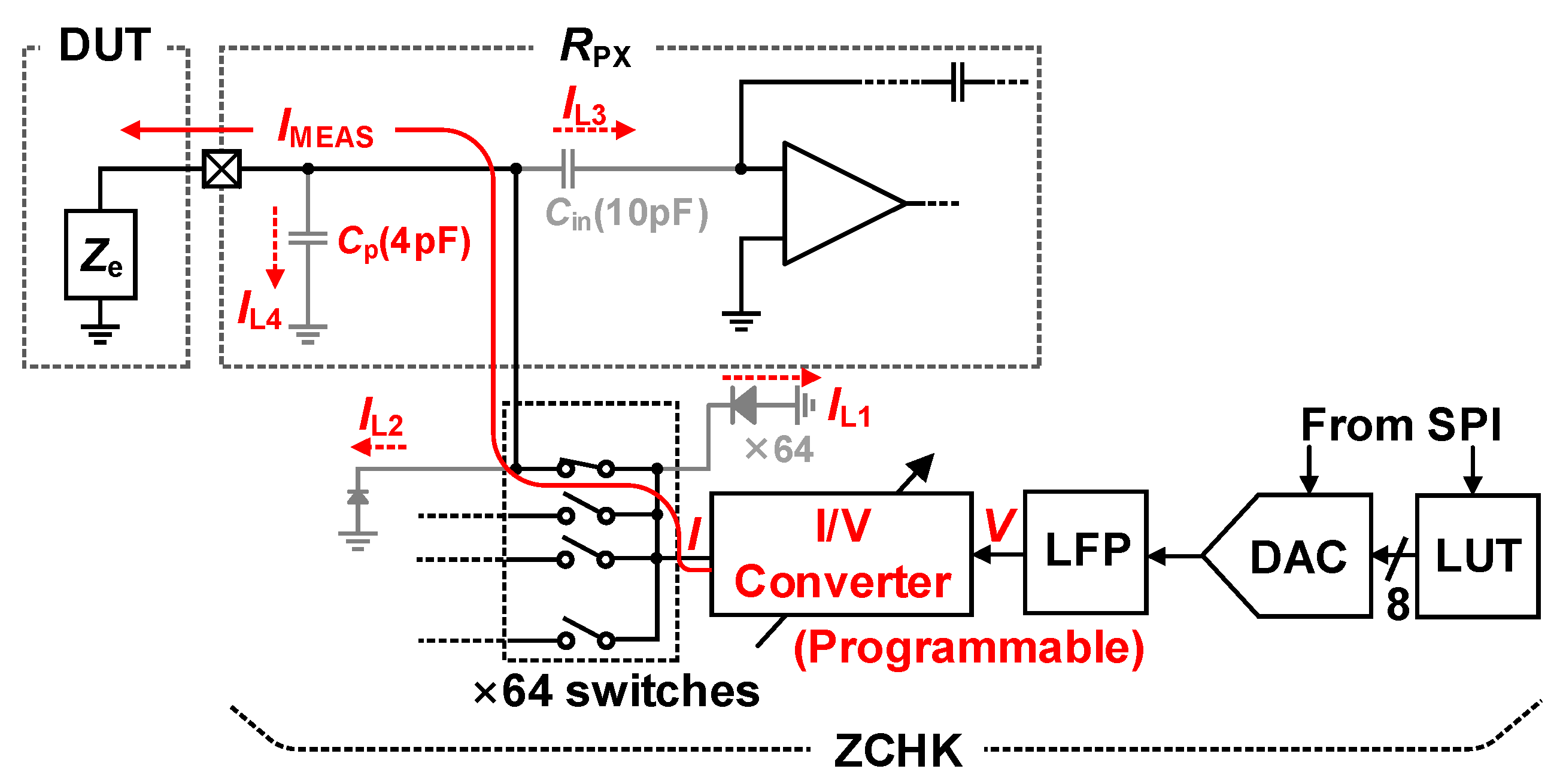
In this work, dedicated ZCHK circuits have been implemented for every 64-channel, as shown in Figure 12. A DAC receives 8 b, 1 kHz sinusoidal commands from a built-in look-up-table (LUT), and converts it into a voltage waveform with a full scale of 1.2 V. After the voltage is smoothed by a second-order LPF, it is converted into current information (IMEAS) in the I-V converter, then applied to the device under test (DUT) through a selected switch. Since the product of the ZE and IMEAS generates a sinusoidal voltage waveform, the RPX dedicated to the DUT amplifies, filters, and digitizes it like a normal neural signal recording.
One of the most critical design factors to be considered for the ZCHK is the resolution for the circuit. The maximum IMEAS provided by the circuit is determined by the input dynamic range of the RPX and the range of measurable ZE, which are ~10 mVpp and 50 kΩ to 10 MΩ in this design. Thus, IMEAS should be in the range of 1 to 200 nA. At the same time, the minimum value of the IMEAS must be much larger than the leakage currents (IL1-4) in the path. According to the SPECTRE simulation with parasitic extraction, the largest leakage current occurs from the Cin of 10 pF in the LNA (IL3), that is <100 pA. Therefore, we designed the I/V converter to be programmable in real time by the SPI to generate output current (I) from 0.5 nA to 50 nA, and we introduced multi-period (>10–100 periods) and multiple measurements (>10 times) and used the average of the measurements. The DAC is the capacitive 8 b SAR DAC with a unit capacitance of 35 fF. A multi-feedback topology has been adopted for the second-order LPF, thus it requires a single OTA for the implementation. The I/V converter consists of an array of capacitors and switches since it should drive a capacitive load (Cin) in the LNA. The ZE measurement is performed only when there is a request, and then automatically shut down, thus the power consumption of the ZCHK in the normal operation is zero.

3.6. Power Management Unit and β-Multiplier

The PMU circuit consists of seven low dropout regulators (LDOs) for 1.2, 1.5, and 1.8 V used in the RPX and ZE measurements, and for 1.8, 2.5, ±3 V used in the SPX and a low voltage BGR. All supplies except for ±3 V are provided by an external 3.3 V and ±3 V supplies are generated by external ±6 V. The low voltage BGR produces 0.9 V, which becomes the reference voltage for the LDOs except for the ±3 V supplies. The BGR also generates all reference currents for the RPX and SPX. The design of the LDOs and BGR are adopted from our previous work [7]. The schematic of the β-multiplier is also adopted from [28] and modified.

4. Measurement

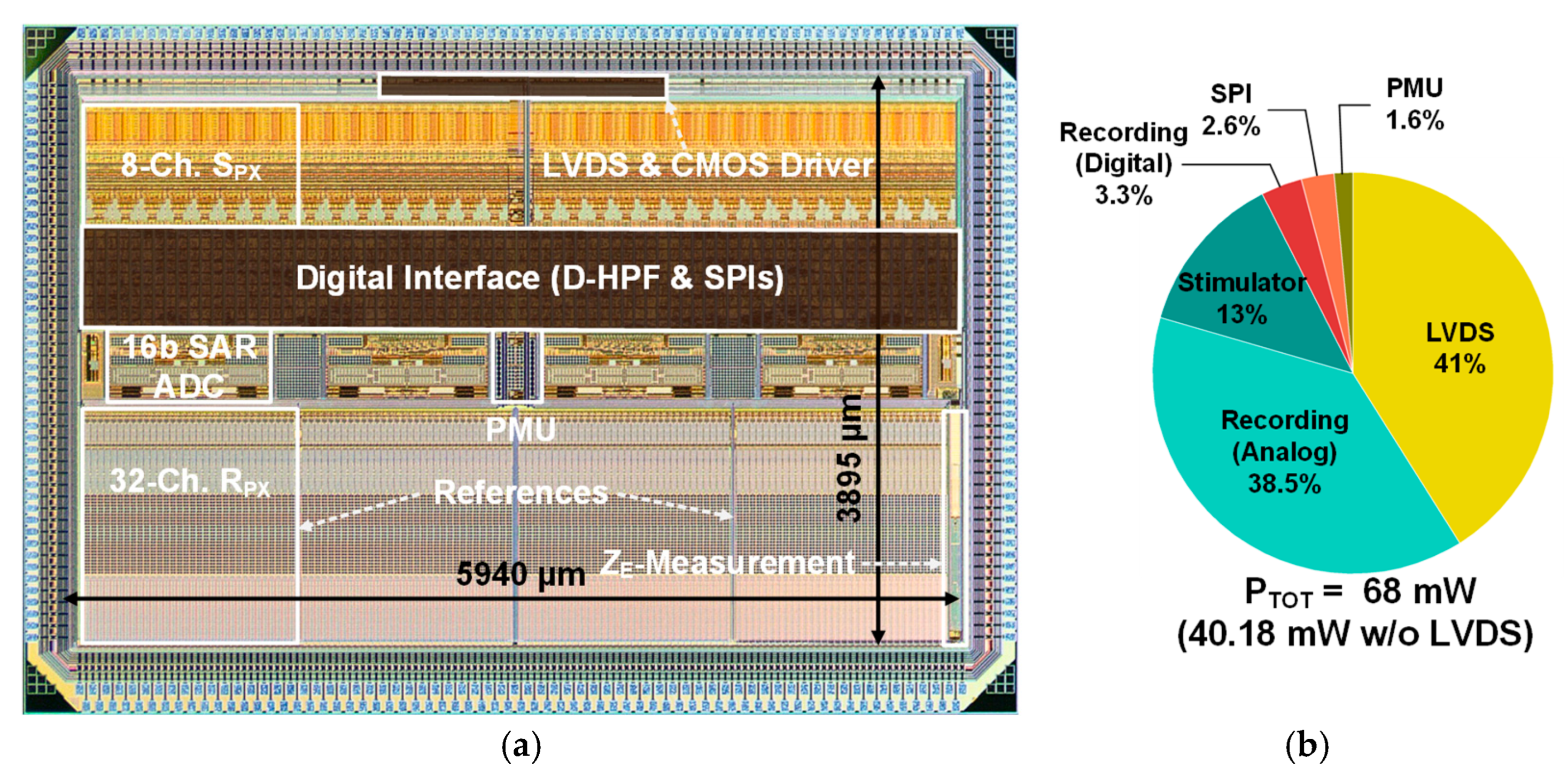
The proposed neuromodulation SoC has been fabricated using a 180 nm 1P6M CMOS process. A microphotograph of the fabricated chip is shown in Figure 13a, where the key circuit blocks are highlighted for visualization. The total active area occupied by the ASIC is 5940 × 3895 μm2, excluding pads. The area must accommodate a large number of inputs, specifically 128 separate inputs and 4 reference inputs, all of which are directed toward the bottom side of the chip with staggered pads. Figure 13b depicts the power consumption breakdown. Total power consumption is 40.18 mW except for the LVDS drivers, which are used only when driving a meter-long cable. The LVDS drivers consume ~28 mW.

4.1. Recording Pixel (RPX) and ADC Measurement

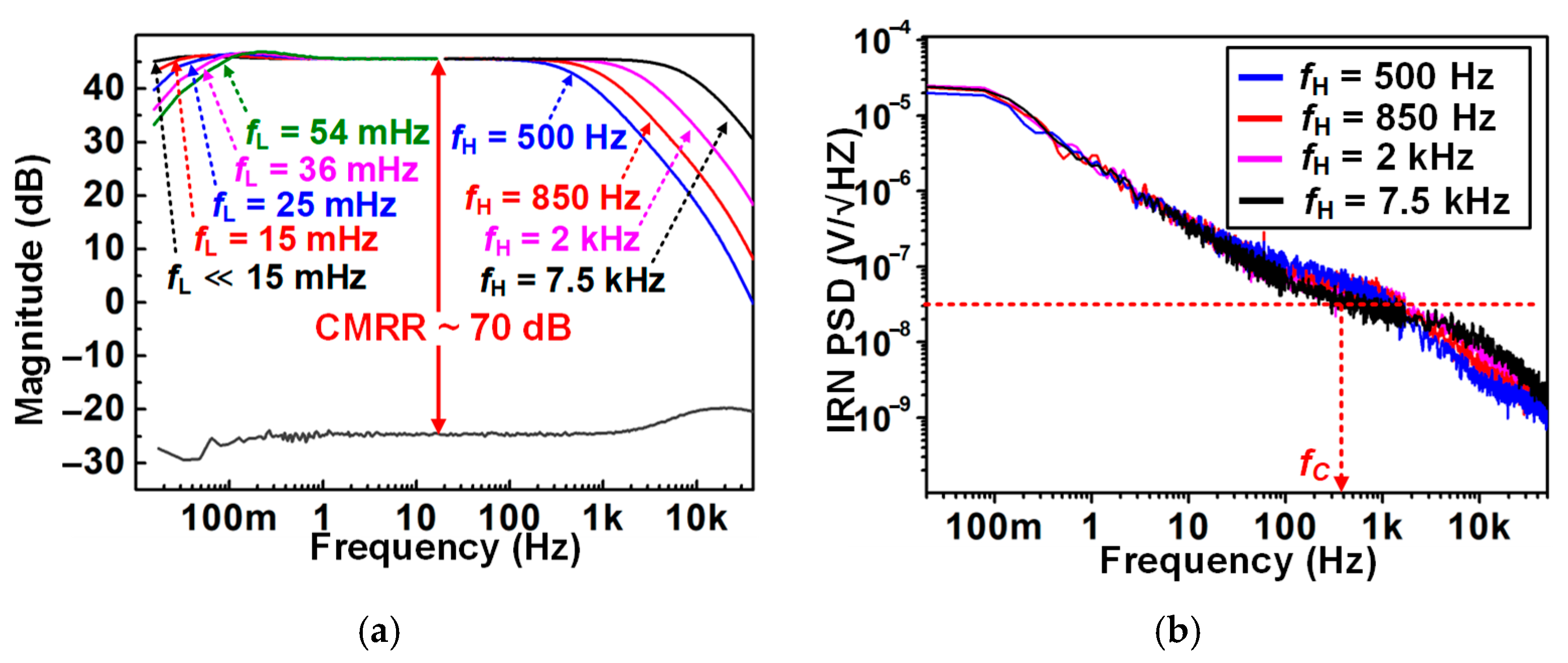
Figure 14a shows the frequency response of a representative single channel RPX measured with a dynamic signal analyzer (35670A, Agilent, Washington, USA). It exhibits a mid-band gain (G) of approximately 45.5 dB (~190 V/V) and >60 dB common mode rejection ratio (CMRR) with a bandwidth spanning from sub-Hz to 8 kHz—sufficient to simultaneously capture both LFPs and APs. The fL is digitally programmable from <<15 mHz to 54 mHz. The fH is also reconfigurable, enabling selectable high-frequency limits of 0.5, 0.85, 1, or 7.5 kHz. Figure 14b shows the IRN spectra of the RPX measured from 0.4 Hz to 50 kHz frequencies. The estimated 1/f-noise corner frequency (fC) is ~300 Hz, and the thermal noise floor reaches approximately 30 nV/√Hz. The LFP (0.1 Hz–0.5 kHz), AP (300 Hz–7.5 kHz), and full band (0.1 Hz–7.5 kHz) noises are ~4.6, ~1.8, and ~4 μVrms, respectively. All numbers indicate that the noise is low enough to measure neural signals in bands.
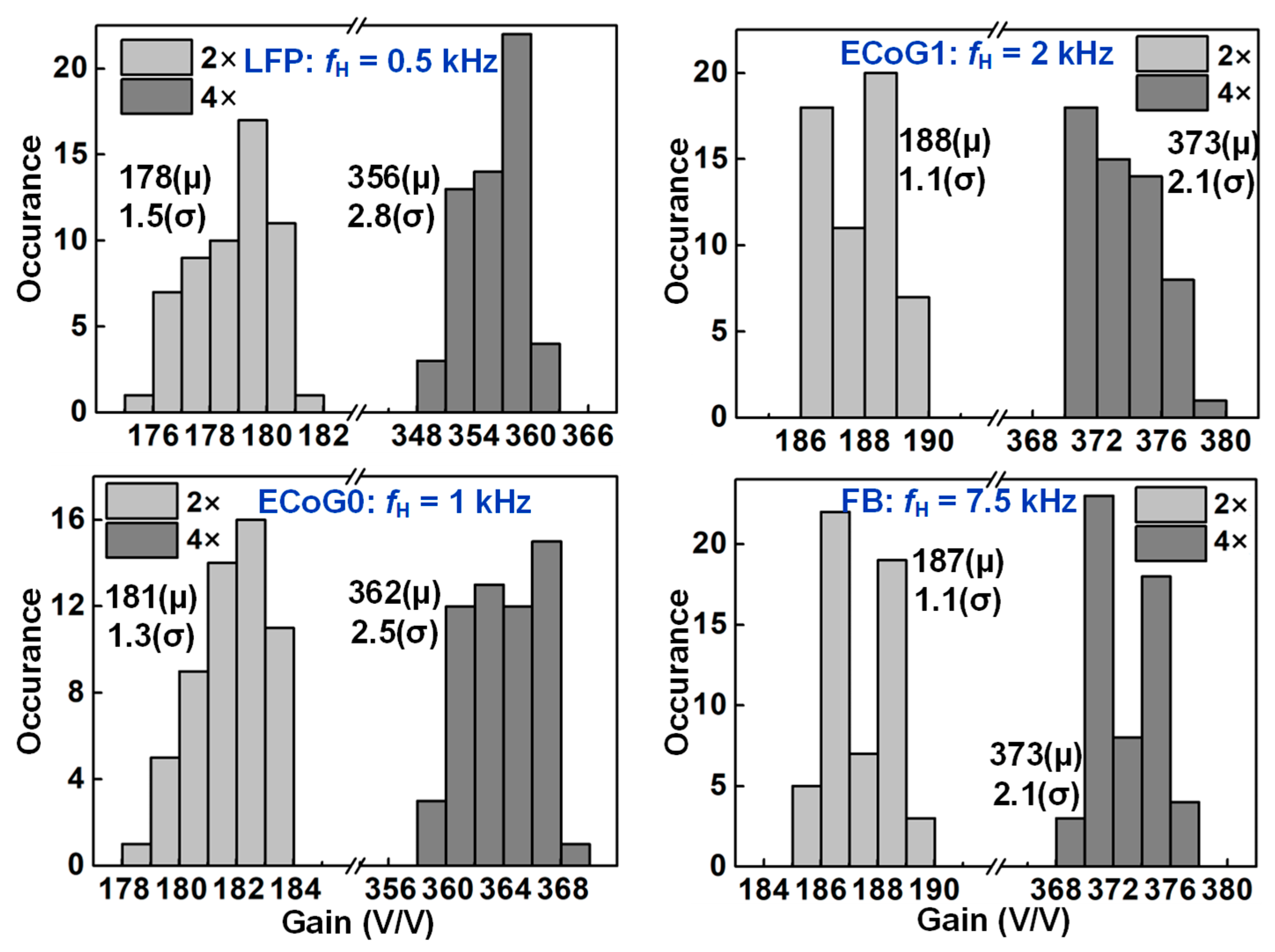
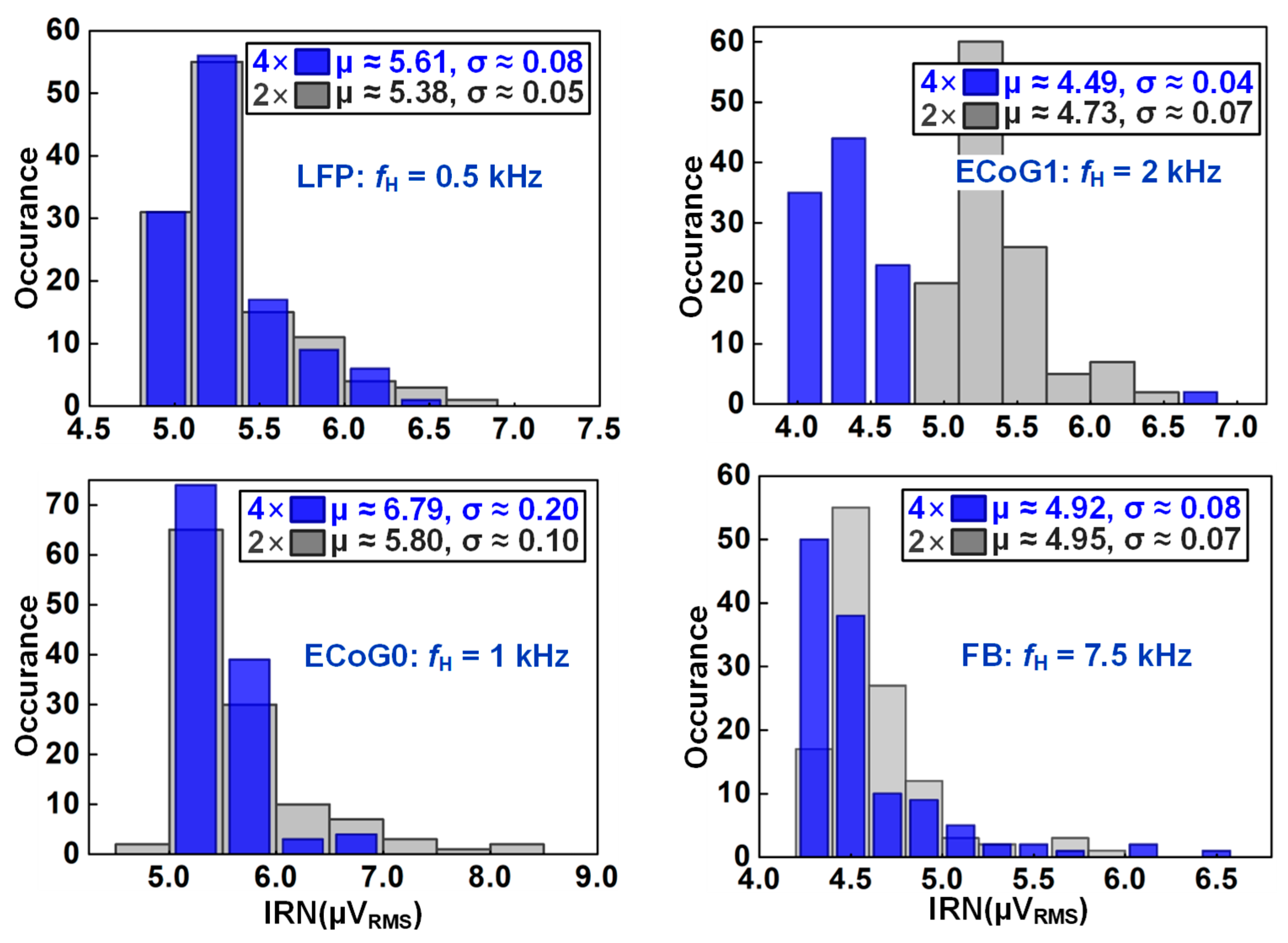
Figure 15 shows the gain distributions of the entire 128 channels according to different gain and fH sets. Inside each figure, the mean (µ) and standard deviation (σ) are also denoted. The gain spread is very narrow (e.g., ~0.898% in the worst case: LFP with 2× gain set), showing decent channel uniformity. Figure 16 shows the noise distribution of the entire channels with different PGA gains and fH. Due to the current scaling according to different fH, the IRN variation is minimal from fH = 0.5 to 7.5 kHz. The larger gain set in the PGA (4×) reduces the noise contribution to the following blocks, such as the buffer and ADC, thus the IRN in this case showed a bit improvement, though it is minor.
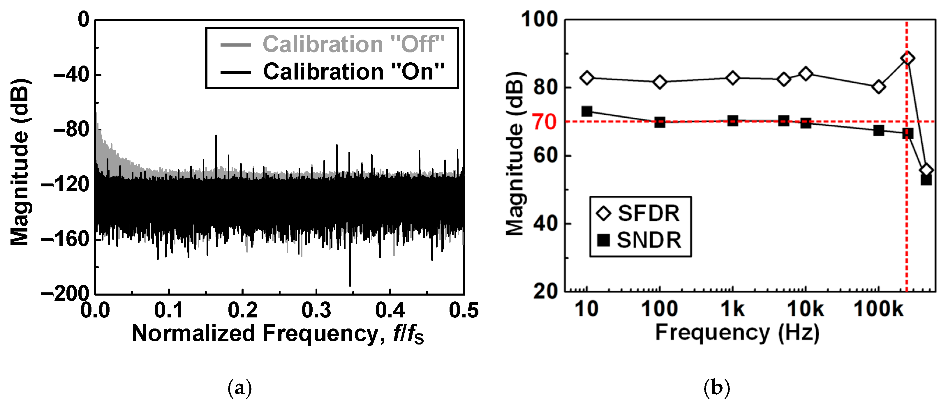
Figure 17a depicts the measured ADC spectra with (black) and without (dark gray) calibration with a −1.94 dBFS, 10 Hz sinusoidal input. Without calibration, the signal-to-noise and -distortion ratio (SNDR), spurious-free dynamic range (SFDR), and total harmonics distortion (THD) was measured as 53.49, 69.38, and −60.42 dB, respectively; those were recovered as 67.72, 82.49, and −76.78 dB with the calibration, indicating the effectiveness of the implemented foreground calibration. The measured SNDR was limited to ~70 dB, which is lower than the theoretical expectation. This discrepancy is attributed to the true single-phase clock (TSPC) dynamic logic used in the SAR controller for area efficiency. We identified that charge leakage in the TSPC gates caused transient glitches, elevating the noise floor. Since the implemented foreground calibration only corrects for static nonlinearities, these dynamic effects were not compensated. Future implementations should consider using static logic to mitigate this issue. Figure 17b shows the SNDR and SFDR versus frequencies from 5 Hz to 600 kHz. Note that the fS of the ADC is 1 MS/s. This ADC shows a stable SNR of ~70 dB up to 10 kHz and exhibits a slight deviation near the fS/4 (~66.62 dB). The effective number of bits (ENOBs) is 11.39 bits at 1 kHz.
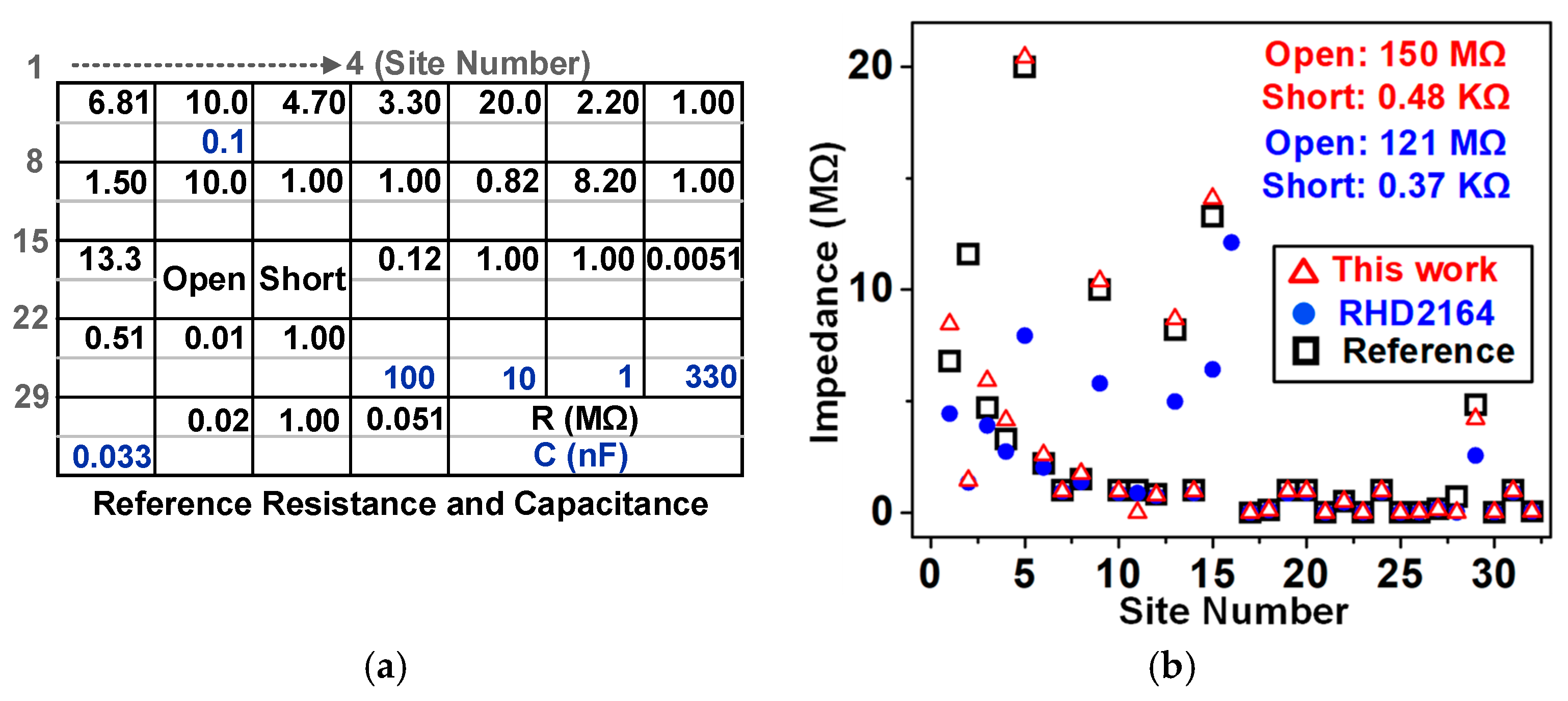
Figure 18 shows the measured results of the ZCHK circuit in comparison with a commercial product (RHD 2164, Intan Technologies, Los Angeles, CA, USA) that has a similar function [32]. For this measurement, a reference module where 32 combinations of different resistors and capacitors for a calibration of another commercial electrode impedance measurement instrument (NanoZTM, Plexon, Dallas, TX, USA) have been employed [33], as shown in Figure 18a. Overall, the two circuits work well for low impedance; however, the implemented circuit exhibits better accuracy regardless of the magnitude of the impedance, while the commercial product showed some deviations when the electrode impedance was high (~10 MΩ).

4.2. Stimulation Pixel (SPX) Measurement

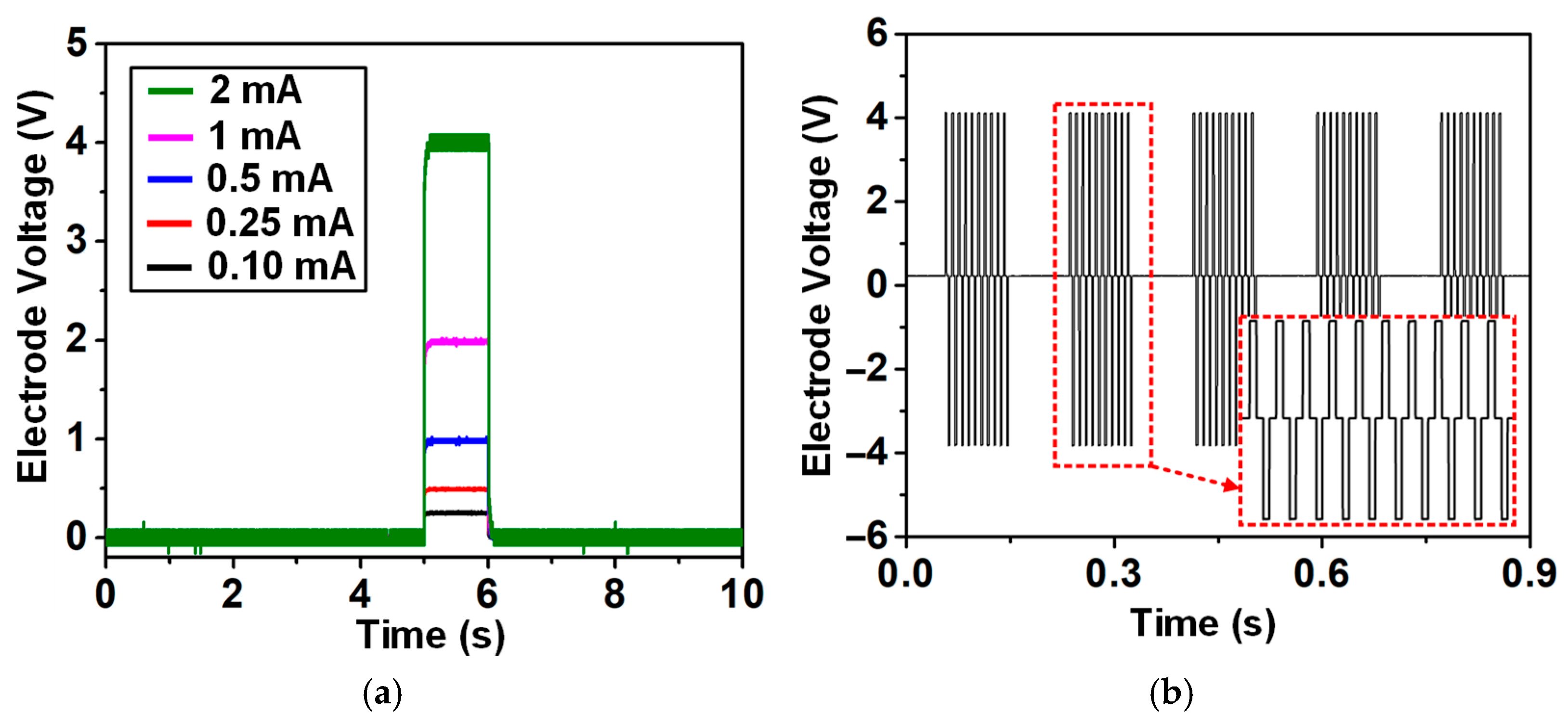
Figure 19a shows the IA control using the different codes in the DAC (10× gain in the I-Amp). As shown, 0.1024 to 2.048 mA has been successfully delivered into a 2 kΩ resistive load. Figure 19b depicts a programmable pulse train of IA and IC (10 pulses) Each stimulation cycle consists of a 500 µs cathodic phase (tC), a 500 µs inter-phase delay (tD), and a 500 µs anodic phase (tA), with a stimulation amplitude of 2 mA. The inset shows the enlarged pulse trains.
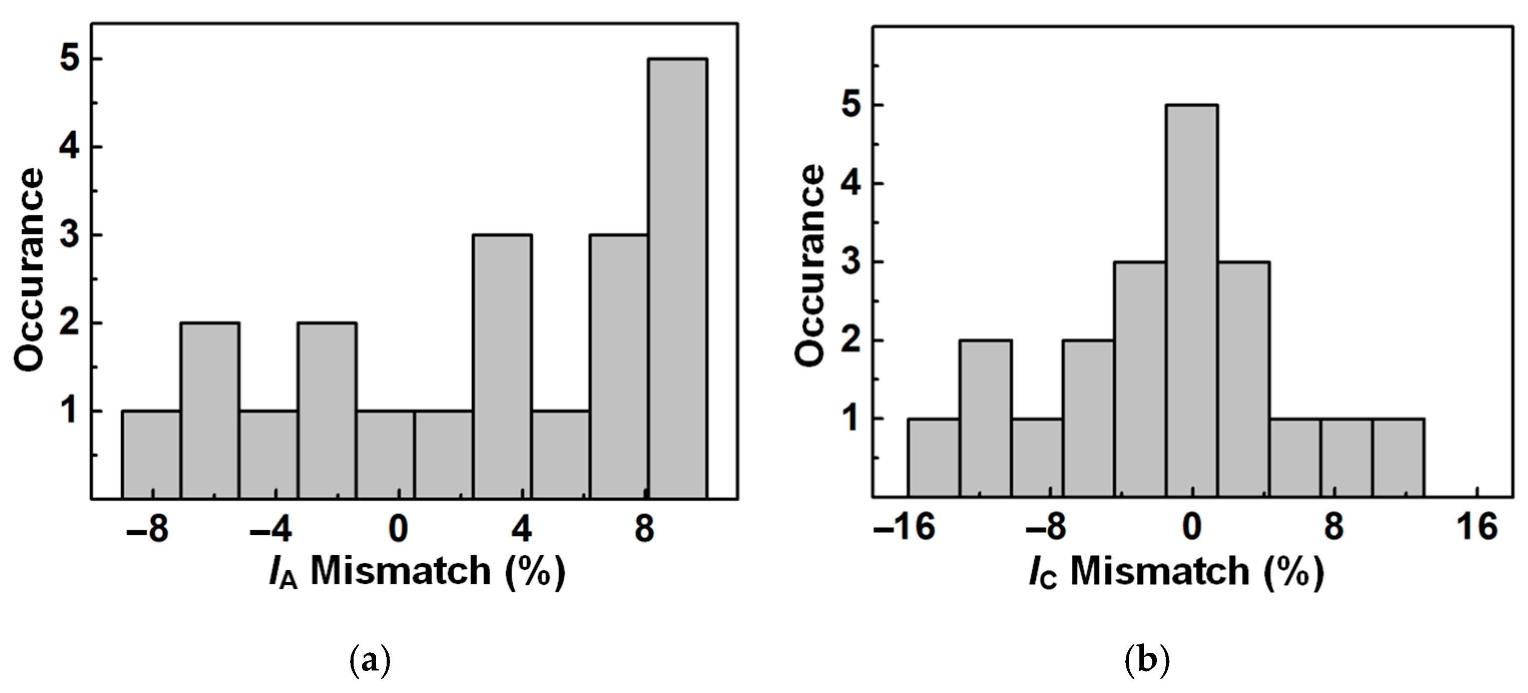
Figure 20 illustrates mismatches of IA and IC from the entire 32-channel SPX when each channel is programmed to generate 1 mA output current. Overall, the mismatches lie within ±10%; however, some channels generating IC show >10%. This mismatch would not affect the safety of the electrode thanks to the charge balancing switch that can eliminate the leftover charge.

4.3. In Vitro Measurement and Summary

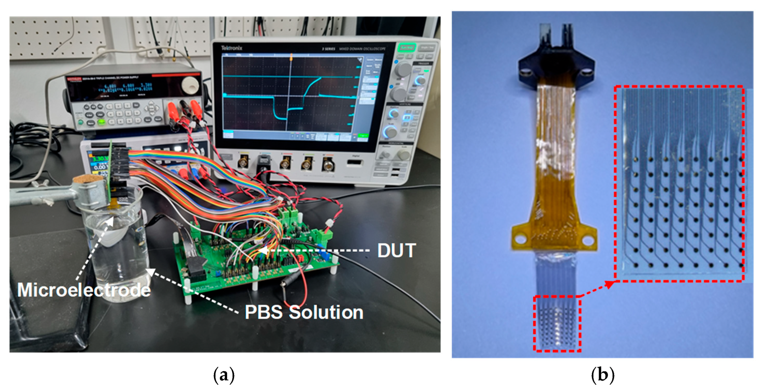
The signal acquisition performance of the fabricated ASIC has also been evaluated in an in vitro environment. A custom-designed silicon neural probe [34], interfaced with the ASIC, was immersed in a phosphate-buffered saline (PBS) solution along with reference and ground electrodes. To emulate biological neural activity, a set of previously recorded neural signals—acquired from the motor cortex of a rat—were replayed through the PBS medium. The overall configuration of the in vitro testing setup and an array of the microelectrode used for the in vitro experiments are shown in Figure 21a and Figure 21b, respectively. For these tests, the ASIC was configured to operate at its maximum bandwidth setting to enable simultaneous recording of both LFPs and APs. The acquired data were transmitted to a host computer via a custom USB-based interface board for subsequent analysis.
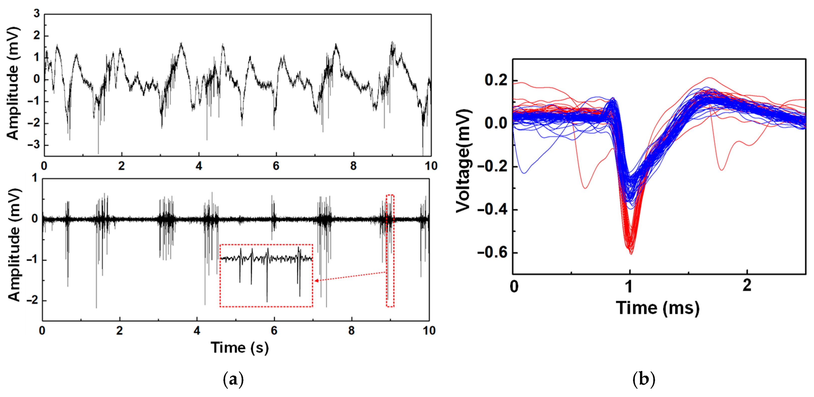
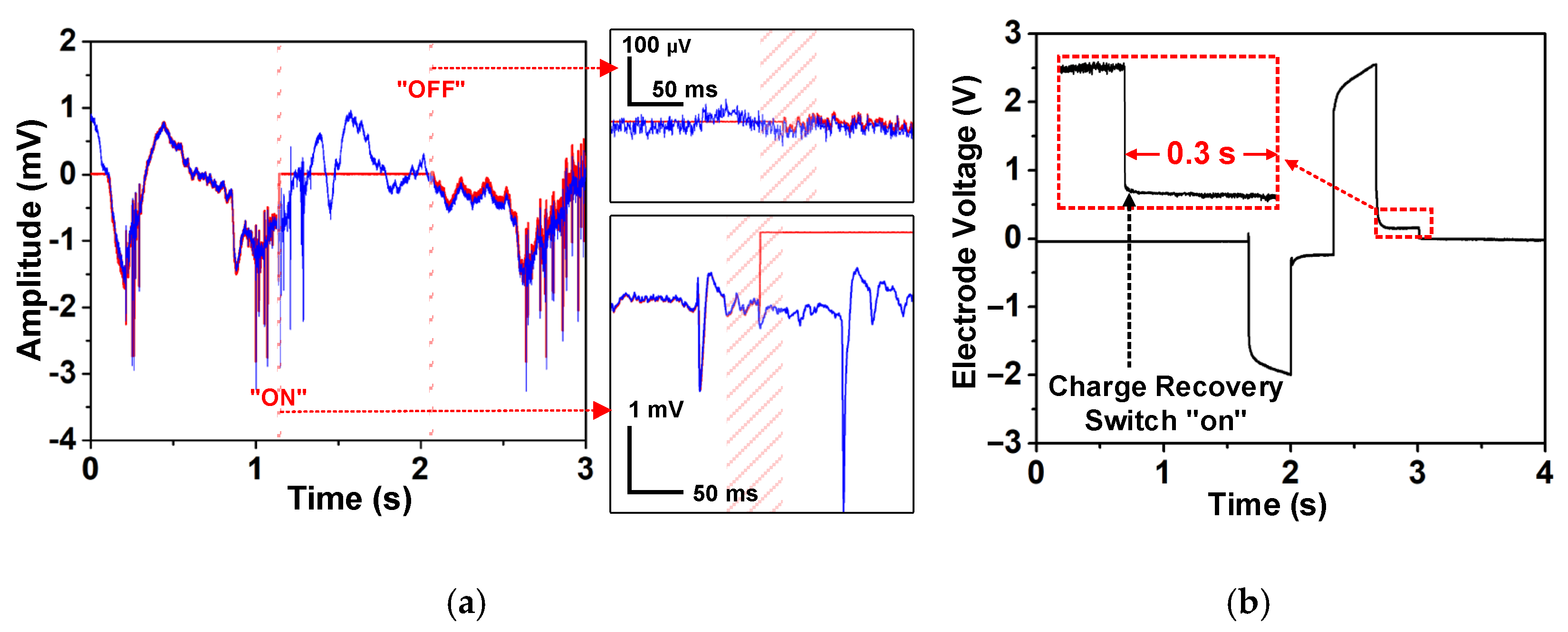
The unprocessed signals are presented in the upper panel of Figure 22a. To enhance signal clarity, the neural recordings were processed using a third-order Butterworth bandpass filter (passband: 0.8–7 kHz; stopband: <0.6 kHz and >8 kHz) implemented in MATLAB (R2025a, MathWorks, Natick, MA, USA). The filtered output, emphasizing AP activity, is shown in the lower panel of Figure 22b where a magnified view of approximately 80 μs of concurrent LFP and AP signals is also provided. Figure 22b depicts the two different APs detected, extracted, and aligned in MATLAB. The clear distinction between the two different APs is attributed to low noise and distortion performance of the RPX. Figure 23a shows the in vitro recording with (red) and without (blue) fast-reset switching operations. After turning off the reset switch, there is no settling delay.
The charge recovery switch for the CB was also verified in vitro. Figure 23b shows the measurement results under a condition where a 20% current mismatch was intentionally introduced. For this experiment, the electrode–tissue interface is modeled using a load comprising a 2 µF double-layer capacitance (CDL) and a 1 kΩ series resistance (RS). When the charge recovery switch is enabled, the electrode potential quickly returns from approximately 160 mV back to 0 V, confirming the effectiveness of the implemented CB mechanism. The estimated on-resistance of the CB switch is ~1 kΩ.
Table 1 summarizes the measurement results and compares them with other state-of-the-art neuromodulation SoCs and a commercial product [35]. In terms of the number of recording and stimulation channels, this work shows the highest number ever reported with reasonable power and area consumption, and the highest density except for [1] and [4]. Furthermore, on a block-level, the recording ASIC achieves a competitive Noise Efficiency Factor (NEF) of 8.9, and the ADC demonstrates a Walden FoM of 100.4 fJ/c-s and a Schreier FoM of 160.4 dB, confirming that high integration was achieved without sacrificing performance efficiency. However, the presented work shows the highest level of integration by including all required circuit blocks on chip and has the largest number of parallel recording and stimulation in a single die. In addition, the proposed SoC is able to operate with a single external supply of 3.3 V and equips important functionalities for neuromodulation, such as ZCHK, fast-reset, LVDS, and CB.

5. Conclusions

This paper presents a fully integrated neuromodulation ASIC that combines a 128-channel neural recording system with a 32-channel current-mode stimulator on a single chip, fabricated using a standard 180 nm CMOS process. The proposed system supports bi-directional neural interfacing, enabling simultaneous high-fidelity neural signal acquisition and precise electrical stimulation, making it suitable for a wide range of neuroscience and clinical applications. The analog front-end (AFE) employs a capacitive-coupled LNA architecture with a digitally programmable bandwidth via a 2-bit current DAC, achieving an input-referred noise of 3.8 μVrms while consuming only 682 μW per channel. The PGA provides two gain settings, and a 16-bit SAR ADC with foreground calibration enables high-resolution digitization at sampling rates up to 30 kS/s. An area- and power-efficient digital high-pass filter (D-HPF) and SPI-based digital controller further contribute to compact system integration. On the stimulation side, the 32-channel current-mode stimulator supports a wide current range (4 μA to 2 mA) using a 9-bit R-2R DAC, current amplifier, and high-voltage current driver with ±6 V compliance. A passive discharge switch is included in each pixel to ensure charge balancing and stimulation safety. Measurement results confirm accurate current delivery, programmable waveform generation, and robust passive charge balancing even under deliberate mismatch conditions. In vitro testing further verifies the recording functionality under biological-like conditions. Compared with existing state-of-the-art solutions, the proposed ASIC offers a high degree of integration and configurability while maintaining low power consumption and high signal quality. This work demonstrates a promising platform for future bi-directional closed-loop neural interface systems aimed at both research and clinical neuromodulation therapies.

Author Contributions

Conceptualization, G.P. and S.-Y.P.; methodology, G.P. and J.K.; software, J.C.; validation, G.P., J.K., J.C., and D.K.; formal analysis, G.P. and J.C.; investigation, G.P., J.C.; data curation, J.C. and B.Y.; writing—original draft preparation, G.P.; writing—review and editing, G.P., J.K., M.K. (Minjae Kim), M.K. (Minsung Kim), B.Y., J.C., D.K., and S.-Y.P.; visualization, J.C. and G.P.; supervision, S.-Y.P.; project administration, S.-Y.P.; funding acquisition, S.-Y.P. All authors have read and agreed to the published version of the manuscript.

Funding

This research was supported by the Challengeable Future Defense Technology Research and Development Program through the Agency For Defense Development (ADD) funded by the Defense Acquisition Program Administration (DAPA) in 2022(No. 915069201), the Seoul R&BD Program (BT240032) and also by BK21PLUS, Creative Human Resource Education and Research Programs for ICT Convergence in the 4th Industrial Revolution.

Data Availability Statement

Data are contained within this article. The raw data supporting the conclusions of this article will be made available by the author on request.

Acknowledgments

The EDA Tools was supported by IC Design Education Center (IDEC).

Conflicts of Interest

The authors declare no conflicts of interest.

References

  1. Biederman, W.; Yeager, D.J.; Narevsky, N.; Leverett, J.; Neely, R.; Carmena, J.M.; Alon, E.; Rabaey, J.M. A 4.78 mm2 Fully-Integrated Neuromodulation SoC Combining 64 Acquisition Channels with Digital Compression and Simultaneous Dual Stimulation. IEEE J. Solid State Circuits 2015, 50, 1038–1047. [Google Scholar] [CrossRef]
  2. Reich, S.; Sporer, M.; Haas, M.; Becker, J.; Schuttler, M.; Ortmanns, M. A High-Voltage Compliance, 32-Channel Digitally Interfaced Neuromodulation System on Chip. IEEE J. Solid State Circuits 2021, 56, 2476–2487. [Google Scholar] [CrossRef]
  3. Pu, H.; Malekzadeh-Arasteh, O.; Danesh, A.R.; Nenadic, Z.; Do, A.H.; Heydari, P. A CMOS Dual-Mode Brain-Computer Interface Chipset with 2-mV Precision Time-Based Charge Balancing and Stimulation-Side Artifact Suppression. IEEE J. Solid State Circuits 2022, 57, 1824–1840. [Google Scholar] [CrossRef]
  4. Zhou, A.; Santacruz, S.R.; Johnson, B.C.; Alexandrov, G.; Moin, A.; Burghardt, F.L.; Rabaey, J.M.; Carmena, J.M.; Muller, R. A Wireless and Artefact-Free 128-Channel Neuromodulation Device for Closed-Loop Stimulation and Recording in Non-Human Primates. Nat. Biomed. Eng. 2019, 3, 15–26. [Google Scholar] [PubMed]
  5. Oh, S.; Kim, K.; Lopez Ruiz, J.R.; Slager, N.; Ko, E.; Vöröslakos, M.; Yoon, E. A compact, ultrahigh-density headstage with high-fidelity hybrid integration for large-scale deep-brain opto-electrophysiology. bioRxiv 2023. [Google Scholar] [CrossRef]
  6. Uehlin, J.P.; Smith, W.A.; Pamula, V.R.; Pepin, E.P.; Perlmutter, S.; Sathe, V.; Rudell, J.C. A Single-Chip Bidirectional Neural Interface with High-Voltage Stimulation and Adaptive Artifact Cancellation in Standard CMOS. IEEE J. Solid State Circuits 2020, 55, 1749–1761. [Google Scholar] [CrossRef]
  7. Park, S.-Y.; Na, K.; Voroslakos, M.; Song, H.; Slager, N.; Oh, S.; Seymour, J.P.; Buzsaki, G.; Yoon, E. A Miniaturized 256-Channel Neural Recording Interface with Area-Efficient Hybrid Integration of Flexible Probes and CMOS Integrated Circuits. IEEE Trans. Biomed. Eng. 2021, 69, 334–346. [Google Scholar] [CrossRef]
  8. Iwai, A.; Tanaka, M. Particle-Aligned Anisotropic Conductive Film (PAL-ACF) for Fine Pitch Interconnection; Hitachi Chemical: Tokyo, Japan, 2017. [Google Scholar]
  9. Jochum, T.; Denison, T.; Wolf, P. Integrated Circuit Amplifiers for Multi-Electrode Intracortical Recording. J. Neural Eng. 2009, 6, 012001. [Google Scholar] [CrossRef]
  10. Harrison, R.R.; Charles, C. A Low-Power Low-Noise CMOS Amplifier for Neural Recording Applications. IEEE J. Solid State Circuits 2003, 38, 958–965. [Google Scholar] [CrossRef]
  11. Song, S.M.; Kim, M.J.; Kim, J.G.; Park, H.T.; Park, Y.H.; Sik, K. 128-Channel Recording, 32-Channel Stimulation, Digitally Interfaced Optogenetic Neuromodulation System-on-Chip. IDEC J. Integr. Circuits Syst. 2022, 8, 1–9. [Google Scholar]
  12. Park, S.-Y.; Cho, J.; Na, K.; Yoon, E. Modular 128-Channel Δ-ΔΣ Analog Front-End Architecture Using Spectrum Equalization Scheme for 1024-Channel 3-D Neural Recording Microsystems. IEEE J. Solid State Circuits 2018, 53, 501–514. [Google Scholar] [CrossRef]
  13. Kim, H.-J.; Park, Y.; Eom, K.; Park, S.-Y. An Area- and Energy-Efficient 16-Channel, AC-Coupled Neural Recording Analog Frontend for High-Density Multichannel Neural Recordings. Electronics 2021, 10, 1972. [Google Scholar] [CrossRef]
  14. Ahuja, B.K. An Improved Frequency Compensation Technique for CMOS Operational Amplifiers. IEEE J. Solid State Circuits 1983, 18, 629–633. [Google Scholar]
  15. Hogervorst, R.; Tero, J.P.; Eschauzier, R.G.H.; Huijsing, J.H. A Compact Power-Efficient 3 V CMOS Rail-to-Rail Input/Output Operational Amplifier for VLSI Cell Libraries. IEEE Int. Solid State Circuits Conf. 1994, 29, 1505–1513. [Google Scholar] [CrossRef]
  16. Ginsburg, B.P.; Chandrakasan, A.P. 500-MS/s 5-bit ADC in 65-nm CMOS with Split Capacitor Array DAC. IEEE J. Solid State Circuits 2007, 42, 739–747. [Google Scholar]
  17. Harpe, P.; Huang, X.; Wang, X.; Dolmans, G.; De Groot, H. A 26 μW 8 bit 10 MS/s Asychronous SAR ADC for Low Energy Radios. IEEE J. Solid State Circuits 2011, 46, 7–10. [Google Scholar]
  18. Miyahara, M.; Asada, Y.; Paik, D.; Matsuzawa, A. A Low-Noise Self-Calibrating Dynamic Comparator for High-Speed ADCs. In Proceedings of the IEEE Asian Solid-State Circuits Conference, Fukuoka, Japan, 3–5 November 2008; pp. 269–272. [Google Scholar]
  19. McNeill, J.A.; Chan, K.Y.; Coln, M.C.W.; David, C.L.; Brenneman, C. All-digital background calibration of a successive approximation ADC using the split ADC architecture. IEEE Trans. Circuits Syst. I Regul. Pap. 2011, 58, 2355–2365. [Google Scholar] [CrossRef]
  20. Liu, W.; Huang, P.; Chiu, Y. A 12-bit, 45-MS/s, 3-mW Redundant Successive-Approximation-Register Analog-to-Digital Converter with Digital Calibration. IEEE J. Solid State Circuits 2011, 46, 2661–2672. [Google Scholar]
  21. Shen, J.; Shikata, A.; Fernando, L.D.; Guthrie, N.; Chen, B.; Maddox, M.; Coln, M.C. A 16-bit 16-MS/s SAR ADC with On-Chip Calibration in 55-nm CMOS. IEEE J. Solid-State Circuits 2018, 53, 1149–1160. [Google Scholar] [CrossRef]
  22. Gagliardi, F.; Scintu, D.; Piotto, M.; Bruschi, P.; Dei, M. Static-Linearity Enhancement Techniques for Digital-to-Analog Converters Exploiting Optimal Arrangements of Unit Elements. IEEE Trans. Very Large Scale Integr. Syst 2024, 32, 2243–2256. [Google Scholar]
  23. Fan, H.; Li, J.; Maloberti, F. Order Statistics and Optimal Selection of Unit Elements in DACs to Enhance the Static Linearity. IEEE Trans. Circuits Syst. I Regul. Pap. 2020, 67, 2193–2203. [Google Scholar] [CrossRef]
  24. Merrill, D.R.; Bikson, M.; Jefferys, J.G.R. Electrical stimulation of excitable tissue: Design of efficacious and safe protocols. J. Neurosci. Methods 2005, 141, 171–198. [Google Scholar] [CrossRef] [PubMed]
  25. Georgiou, J.; Toumazou, C. A 126-μW Cochlear Chip for a Totally Implantable System. IEEE J. Solid-State Circuits 2005, 40, 430–443. [Google Scholar] [CrossRef]
  26. Lopes, E.M.; Rego, R.; Rito, M.; Chamadoira, C.; Dias, D.; Cunha, J.P.S. Estimation of ANT-DBS Electrodes on Target Positioning Based on a New PerceptTM PC LFP Signal Analysis. Sensors 2022, 22, 6601. [Google Scholar] [CrossRef]
  27. Plachta, D.T.T.; Gierthmuehlen, M.; Cota, O.; Boeser, F.; Stieglitz, T. BaroLoop: Using a multichannel cuff electrode and selective stimulation to reduce blood pressure. In Proceedings of the 2013 35th Annual International Conference of the IEEE Engineering in Medicine and Biology Society (EMBC), Osaka, Japan, 3–7 July 2013; pp. 755–758. [Google Scholar]
  28. Razavi, B. Design of Analog CMOS Integrated Circuits; Tsinghua University Press Co., Ltd.: Beijing, China, 2005. [Google Scholar]
  29. Hammerschmied, C.M. CMOS A/D Converters Using MOSFET-Only R-2R Ladders; Swiss Federal Institute of Technology Zurich: Zürich, Switzerland, 2000. [Google Scholar]
  30. Hsieh, C.C.; Ker, M.D. Monopolar Biphasic Stimulator with Discharge Function and Negative Level Shifter for Neuromodulation SoC Integration in Low-Voltage CMOS Process. IEEE Trans. Biomed. Circuits Syst. 2021, 15, 568–579. [Google Scholar] [CrossRef]
  31. Yates, R.; Lyons, R.G. DC Blocker Algorithms. IEEE Signal Process. Mag. 2012, 25, 105–110. [Google Scholar]
  32. Intan Technology. RHD2164 Digital Electrophysiology Interface Chip; Intan Technology: Los Angeles, CA, USA, 2013. [Google Scholar]
  33. Plexon nanoZ User Manual. 2012. Available online: https://plexon.com/wp-content/uploads/2017/06/nanoZ-User-Manual-2012.pdf (accessed on 12 October 2025).
  34. Moon, H.; Jang, J.W.; Park, S.; Kim, J.H.; Kim, J.S.; Kim, S. Soft, conformal PDMS-based ECoG electrode array for long-term in vivo applications. Sens. Actuators B Chem. 2024, 401, 135099. [Google Scholar] [CrossRef]
  35. Intan Technology. RHS2116 Digital Electrophysiology Stimulator/Amplifier Chip; Intan Technology: Los Angeles, CA, USA, 2018. [Google Scholar]
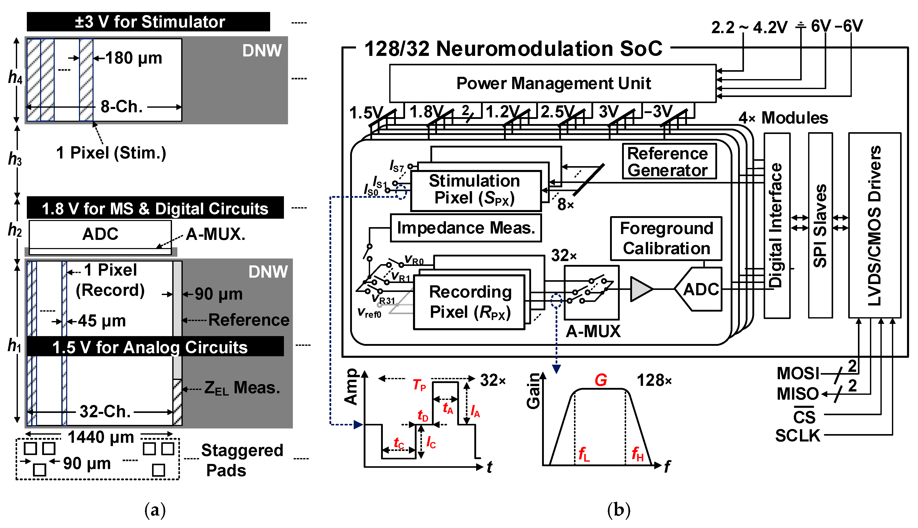
Figure 1. Proposed 128/32-channel neuromodulation SoC: (a) block allocation and layout overview, and (b) block-level circuit architecture.
Electronics 14 04057 g001
Figure 2. Circuit block diagram of a single-channel RPX.
Electronics 14 04057 g002
Figure 3. Transistor-level implementation of the OTA used for the LNA (a), and IRN equivalent circuit (b).
Electronics 14 04057 g003
Figure 4. PGA implementation: (a) circuit block diagram, (b) transistor-level implementation of Gm2 used for the PGA.
Electronics 14 04057 g004
Figure 5. Capacitive DAC used for the 16 b SAR ADC.
Electronics 14 04057 g005
Figure 6. Comparator used for the ADC: (a) preamplifier, (b) two-stage latched-comparator.
Electronics 14 04057 g006
Figure 7. Self-calibration with LSB capacitors as the backend DAC when: (a) (top) calibrating the first capacitor, (bottom) calibrating the higher capacitor, (b) calibrating the MSB capacitor.
Electronics 14 04057 g007
Figure 8. (a) Block diagram for a stimulation pixel (SPX), (b) conceptual cross-sectional view of the PMOS transistor.
Electronics 14 04057 g008
Figure 9. Transistor-level implementation of the LS circuit in the I-Driver.
Electronics 14 04057 g009
Figure 10. Level shifters: (a) 1.8 V to VDDHVSSH, (b) 1.8 V to VDDLVSSL, and (c) VDDLVSSL to 1.8 V.
Electronics 14 04057 g010
Figure 11. (a) Block diagram for 32-channel D-HPF, and (b) High-pass cutoff (fC,HPF) vs. α.
Electronics 14 04057 g011
Figure 12. Circuit block diagram for ZE measurement.
Electronics 14 04057 g012
Figure 13. (a) Microphotograph of the fabricated neuromodulation SoC; (b) Power consumption breakdown.
Electronics 14 04057 g013
Figure 14. Spectral characteristics of the RPX: (a) frequency response with different fL and fH sets, (b) input-referred noise spectra with different fH sets.
Electronics 14 04057 g014
Figure 15. Gain distribution across the entire 128 channels with two gains of the PGA and different sets of fH.
Electronics 14 04057 g015
Figure 16. Noise distribution across the entire 128 channels with two gains of the PGA and different sets of fH.
Electronics 14 04057 g016
Figure 17. (a) Measured spectra of the ADC with and without calibration, (b) SNDR/SFDR performance vs. input frequency.
Electronics 14 04057 g017
Figure 18. ZCHK circuit measurement: (a) reference values of the resistors and capacitors for the measurement, (b) measured results in comparison with a commercial product.
Electronics 14 04057 g018
Figure 19. (a) IA current control from 0.1024 to 2.048 mA, (b) IA and IC current pulse train.
Electronics 14 04057 g019
Figure 20. Distribution of the mismatch between IA and IC: (a) Mismatch of IA, (b) Mismatch of IC.
Electronics 14 04057 g020
Figure 21. In vitro test setup (a), and microelectrode used for the in vitro test (b).
Electronics 14 04057 g021
Figure 22. (a) Broadband (LFP + AP) neural signal recorded in vitro (upper), and the extracted AP (lower), (b) detected, extracted, and aligned AP signals.
Electronics 14 04057 g022
Figure 23. (a) Fast-recovery operation, (b) charge recovery switch operation.
Electronics 14 04057 g023
Table 1. Comparison table of neuromodulation SoCs.
[1][2][3][4][35]This Work
Neuromodulation SoC
(a) # of Channel (R./S.)(b) 64/232/3232/4128/816/16128/32
(c) System IntegrationNYYNYY
ZE MeasurementNYNNYY
Chip area (mm2)4.7824.9130.25(R) + 36(S)
(Two chips)
11.52 × 2
(Two chips)
23.4231.96
Area/Ch (mm2)0.1180.3890.945/60.1690.7320.2
System Power (mW)(d) 6.2(h) 17234.540.18
Power/Ch (mW)(d) 0.194(h) 1.2651.0780.251
Technology65 nm
CMOS
180 nm
BCD
180 nm
BCD
180 nm
BCD
180 nm
CMOS
Recording ASIC
IRN (μVrms)7.53.8/3.3 (LFP/AP)1.03(e) 1.022.4(i) 4
BW (Hz)10–8 k0.2–7.5 k2–200(e) 1–2000.1–20 k0.1–7.5 k
NEF3.63.1/4.5
(LFP/AP)
2.37158.9
fS/Ch. (kS/s)20(e) 0.414030
ADC Resolution (bit)101612151616
ADC ENOB8.212.110.4710.211.39
FoMS (dB)167.1153.2160.4
FoMW (fJ/c−s)4.251170100.4
Supply Voltage (V)1.01.81.01.03.33.3
Fast RecoveryY
(switch)
N
(−)
Y
((f) SSCS)
Y
(Lin. Interp.)
Y
(switch)
Y
(switch)
Stimulation ASIC
Mono (M)-/Bipolar (B)BMMMMM
Resolution (bits)668889
Min. Current (μA)7320.014
Max. current (mA)0.910.212.7552.552
Voltage compliance (V)8±94012±9 (−12/6)±6
Multipolar stim.NYYYYY
Charge BalancingNY
(switch)
Y
((g) TBCB)
Y
(switch)
Y
(switch)
Y
(switch)
(a) R: recording, S: stimulation, (b) up to eight channels covered by multiplexing, (c) system integration indicates that the implementation does not require any external supports except for a single power supply, (d) power consumption in the recording circuit only, (e) estimated based on the given information, (f) SSCS: stimulation-side contour shaping, (g) TBCB: time-based charge balancing, (h) radio power included, (i) full-bandwidht (0.1 Hz–50 kHz) considered.
Disclaimer/Publisher’s Note: The statements, opinions and data contained in all publications are solely those of the individual author(s) and contributor(s) and not of MDPI and/or the editor(s). MDPI and/or the editor(s) disclaim responsibility for any injury to people or property resulting from any ideas, methods, instructions or products referred to in the content.