Abstract
In industries dealing with motor drive systems, the use of real-time simulators for validating control codes is becoming increasingly mandatory. This is particularly essential for systems with advanced control codes or complex microcontroller unit (MCU) register configurations, as this validation process helps prevent accidents and shorten development time. This study presents a validation process using a real-time simulator for the beatless control of six-step operation. Six-step operation, when applied to high-speed drives, has a limitation on the number of samples per electrical rotation, which causes voltage errors. A representative of these voltage error phenomena is the beat phenomenon, resulting in torque ripple at the first harmonic and high current ripple. To mitigate this beat phenomenon, a synchronous PWM method is sometimes used. However, in practical industrial systems, it may not be feasible to synchronously adjust the inverter’s switching frequency with the rotation speed. This study proposes a beatless control method to eliminate the voltage errors caused by the beat phenomenon during six-step operation at a fixed switching frequency. The specific implementation of this control method is explained based on MCU timer register settings. While previous studies have only proposed beatless control methods, this paper goes further by implementing the proposed beatless method using the MCU (TMS320F28335) to generate gating signals and validating the implementation through simulation on a permanent magnet synchronous motor using a real-time simulator (Typhoon HIL).
1. Introduction
The use of real-time simulators in the current industry is expanding rapidly. Initially, real-time simulators were mainly used in large-scale grid-connected systems, such as multilevel systems or modular multilevel converters, which employ a large number of power semiconductors. However, as the use of power conversion systems is increasingly adopted, real-time simulators are being applied to verify the designed control circuits and control codes in advance. With the expansion of electric vehicles (EVs), high-power motor drive systems are increasingly required, and real-time simulators are being used as a tool to validate new control systems and theories. Some electric vehicle manufacturers now mandate the use of real-time simulators for validation before conducting motor drive experiments, which serves as a representative example of real-time simulator applications [1,2,3,4].
Among various power electronics research fields, the greatest challenge in motor drive research lies in establishing a mechanical experimental environment. Dynamometer setups, which are used to test the performance of motors, require high costs, extensive setup time, and large space proportional to the output, making them limited even if such experimental equipment is available. Therefore, motor drive experiments during the development of new control techniques demand careful attention from researchers. However, accidents due to inevitable human errors during experiments can lead to fatalities and, in the case of damage to the experimental environment, may incur high restoration costs and time, significantly increasing research and development duration and expenses. Additionally, while various simulation programs can be utilized, there are limitations in verifying issues that may arise during actual experiments due to differences in the control circuits implemented with MCUs or FPGAs. In this regard, real-time simulators provide an excellent solution.
This study presents a beatless control method for the six-step control of motor drive systems and carries out validation using a real-time simulator. The six-step operation of motors is a control method applied to maximize voltage output during high-speed operation, where the ratio of the inverter voltage output’s base frequency to the sampling frequency can be as high as 10–12, and more recently, controls requiring even lower ratios have emerged [5,6,7,8,9,10,11,12,13,14,15,16,17]. A low sampling frequency compared to the output frequency can lead to voltage output errors, but most of the conventional research has discussed the low-order harmonics of the output voltages and the phase currents in the normal PWM region [5,6,7,8,9,10,11,12,13]. Research on reducing the generation of low-frequency voltage and current in the six-step region has been limited.
The reason for the generation of beat voltage errors in the six-step region is that the electrical rotational frequency of the motor and the switching frequency of the inverter become asynchronous. Therefore, the simplest setting to eliminate these beat voltages is to vary the switching frequency to be a multiple of 6n times the electrical rotational frequency. Although various studies have proposed solutions for variable switching, in actual industrial applications [15,16,17], it may not always be possible to set the variable switching frequency. For example, low-spec MCUs may be used, or communication with other systems may be based on the inverter’s sampling frequency. In [14], a six-step beatless method that can be implemented with a fixed switching frequency was proposed, but since specific implementation methods based on an MCU were not presented, there may be limitations in actually implementing and applying this method.
To eliminate the beat phenomenon in six-step operation, synchronous PWM methods can be applied. However, in systems where it is not possible to adjust the inverter’s switching and sampling frequencies according to the specific application, the use of synchronous PWM is not feasible. This paper proposes a beatless control method to eliminate the beat phenomenon during six-step operation in motor control systems that apply fixed switching and sampling frequencies. The proposed beatless control method differs from conventional carrier-based PWM methods and their operation. Thus, when implementing this method on an MCU system, it is necessary to modify the PWM output register settings, distinguishing between the linear modulation region and other regions. This study presents the PWM-related register settings required for implementing the beatless control on typical motor drive MCUs. The proposed beatless control is implemented using an MCU (TMS320F28335), and its performance is validated through experiments using a real-time simulator (Typhoon HIL).
The remaining chapters of this paper are as follows. Section 2 explains the beat phenomenon that can occur in six-step operation. Section 3 presents the six-step beatless control method and how to implement it based on an MCU. Section 4 investigates the proposed control method using a real-time simulator, and Section 5 concludes the paper with the final remarks.
2. Beat Phenomenon in Six-Step Operation
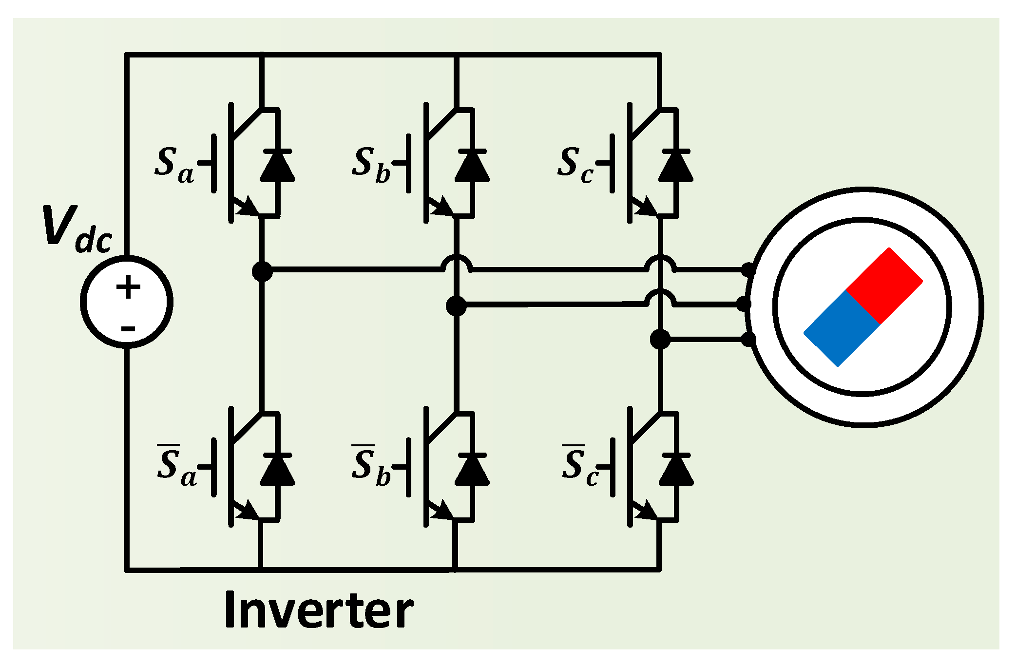
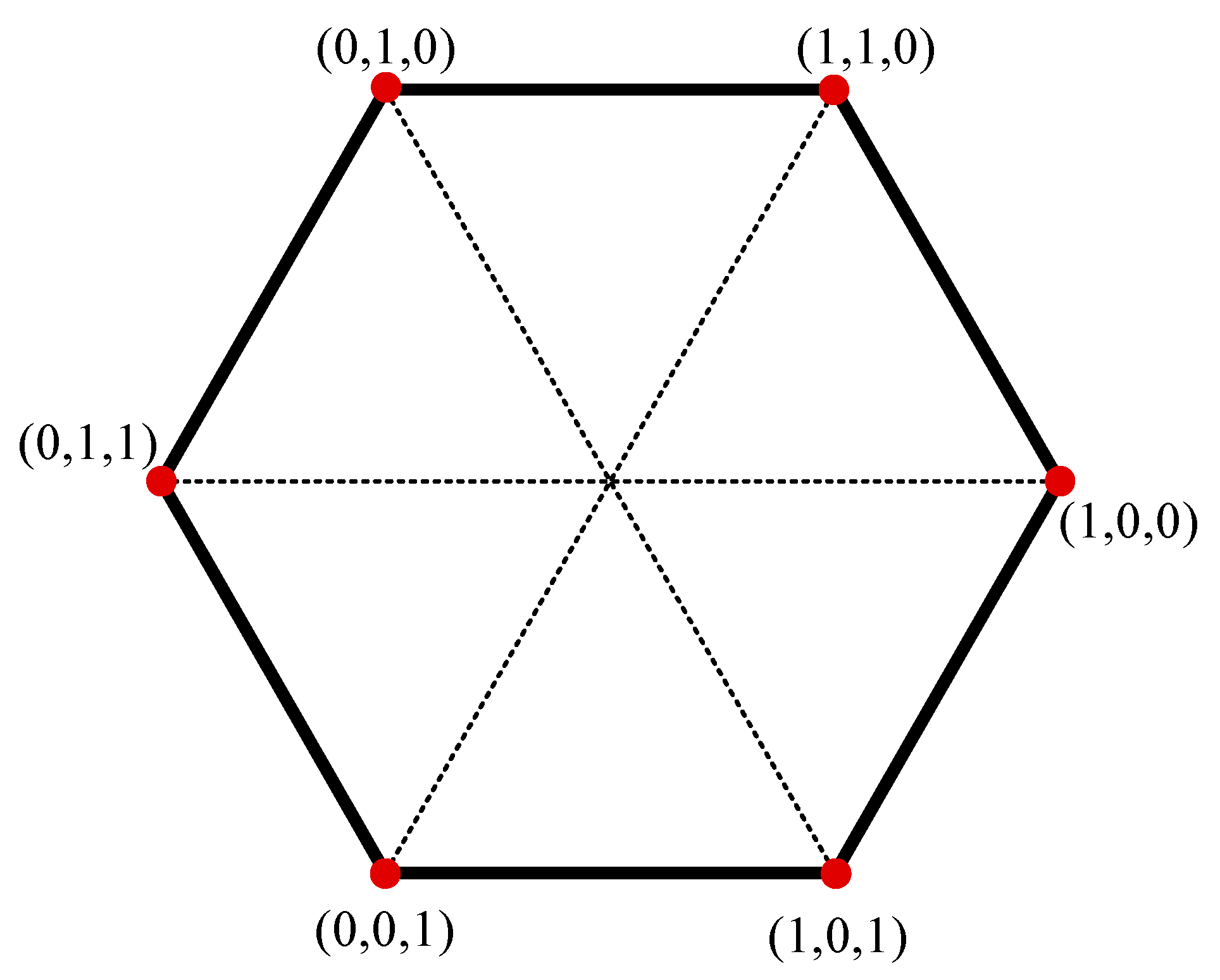
Figure 1 shows the inverter system driving a three-phase AC motor. The voltage vectors output by the three switch legs, depending on their operation, can be represented by the voltage hexagon, as shown in Figure 2. The six vertices of the hexagon represent the valid output voltage vectors generated by the inverter, and the center of the hexagon represents the null voltage vector occurring when all three switch legs are in the same state. In Figure 2, the switching states are represented by (Sa, Sb, Sc), where Sx is represented as 1 when the phase switch is on and 0 when it is off. The three-phase inverter system can output all voltage vectors within the voltage hexagon, and in the six-step control for maximizing the magnitude of the rotating voltage vector for AC motor control, only the six vertex vectors of the hexagon are sequentially output. This section analyzes the changes in switching states and output voltages during the six-step operation.
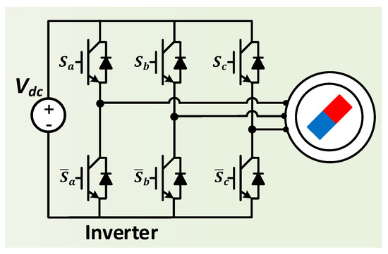
Figure 1.
Three-phase motor drive system with an inverter and permanent magnet synchronous motor.
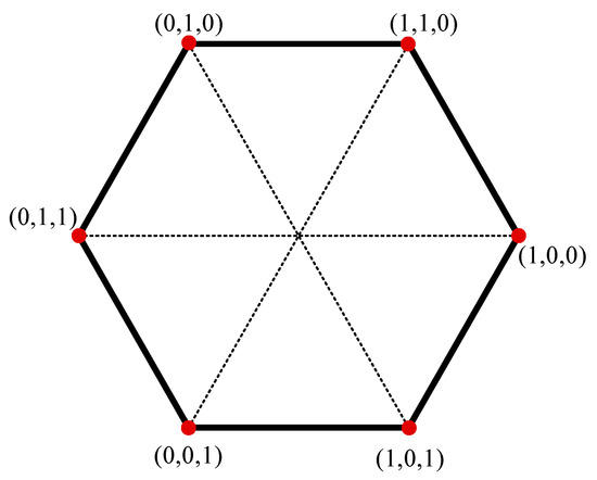
Figure 2.
Voltage hexagon by 3-phase inverter and switching states at six vertex points.
2.1. Ideal Voltage Output in Six-Step Operation
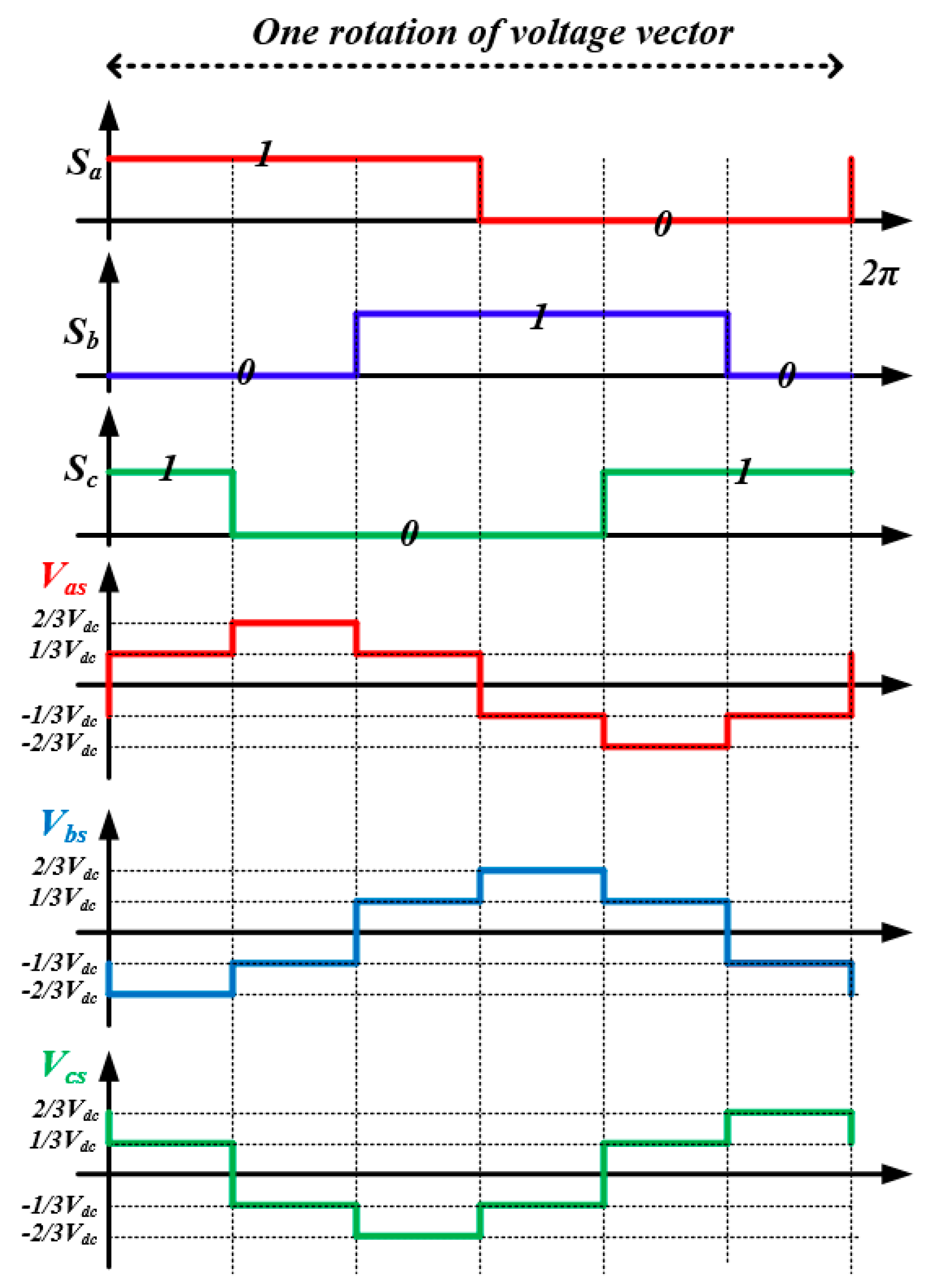
As mentioned above, in the six-step operation, only the six vertex voltage vectors of the voltage hexagon are utilized to operate the motor. At this point, the voltage vector is sequentially modified to the neighboring vertex, and for each rotation of the voltage vector, each phase leg switch performs only one switching operation. Therefore, in the six-step operation, not only the magnitude of the output voltage vector is maximized, but also, the switching losses can be significantly reduced compared to the linear modulation region where each phase leg switches twice per sampling period. Figure 3 shows the gating signals of each phase switch and the output phase voltages for one rotation of the voltage vector.
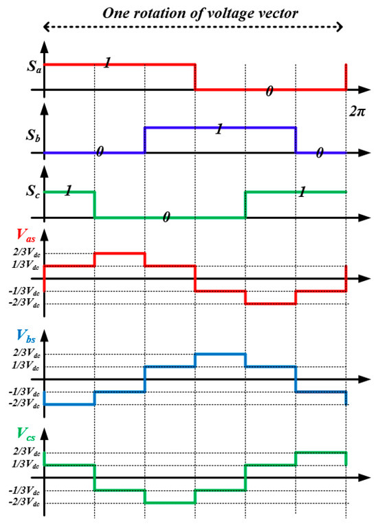
Figure 3.
Switching signals and phase voltages according to synchronous PWM in 6-step operation.
As mentioned above, for each electrical rotation cycle of the motor, each of Sa, Sb, and Sc performs two switchings, respectively, and this operation outputs the six voltage vectors. However, under digital control, which applies the sampling period, the following assumptions are required to achieve the ideal six-step voltage output as shown in Figure 3.
Here, refers to the electrical rotational frequency of the motor rotor, and represents the inverter’s switching frequency or sampling frequency. For the ideal six-step voltage output without error caused by the beat phenomenon, as shown in Figure 3, the inverter’s switching frequency must be 6n times of . Therefore, the conventional synchronous PWM drive systems apply a variable switching frequency method that adjusts the switching and sampling frequencies to satisfy the condition of (1). However, this variable switching frequency method may be limited depending on the MCUs used in various industrial applications. The next section presents the beat voltage error phenomenon due to fixed switching and sampling frequencies and analyzes its impact.
2.2. Beat Phenomenon Due to Fixed Sampling Frequency in Six-Step Operation
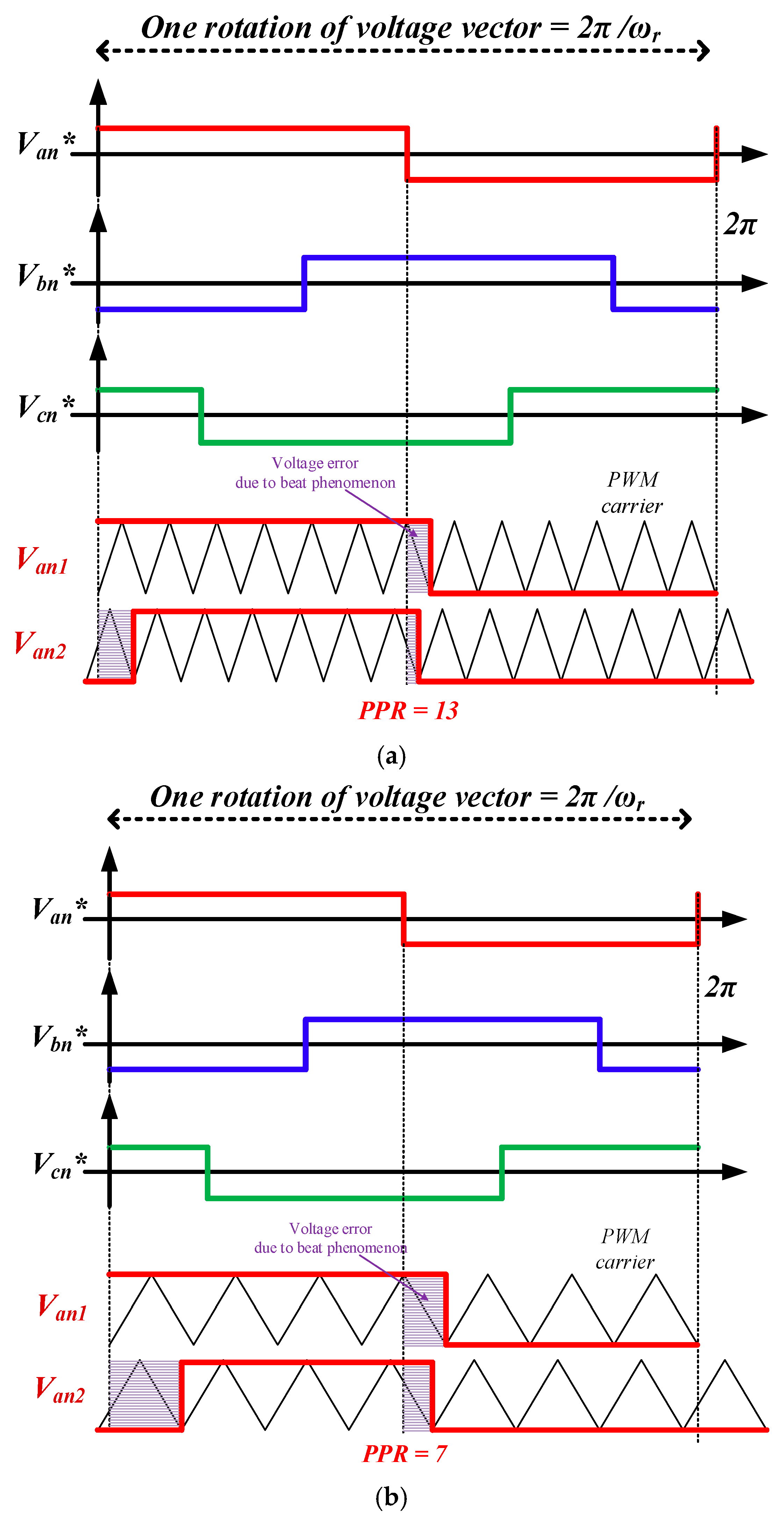
In the case where the synchronous PWM method is not applied in six-step operation, the occurrence of the beat phenomenon is determined by the ratio of the rotational frequency to the switching frequency. For easier analysis, this paper defines PWM pulse per one rotation (PPR) and uses it for voltage output analysis.
In the case of the synchronous PWM mentioned above, PPR satisfies the condition of (1) (multiple of six). However, when a fixed sampling frequency is applied, PPR is determined as an arbitrary integer or real number that is not a multiple of six, resulting in the beat phenomenon. Figure 4a,b show the a-phase pole voltage output (Van1, Van2) for the cases where PPR is 13 and 7, respectively, according to the pole voltage reference (Vam*).
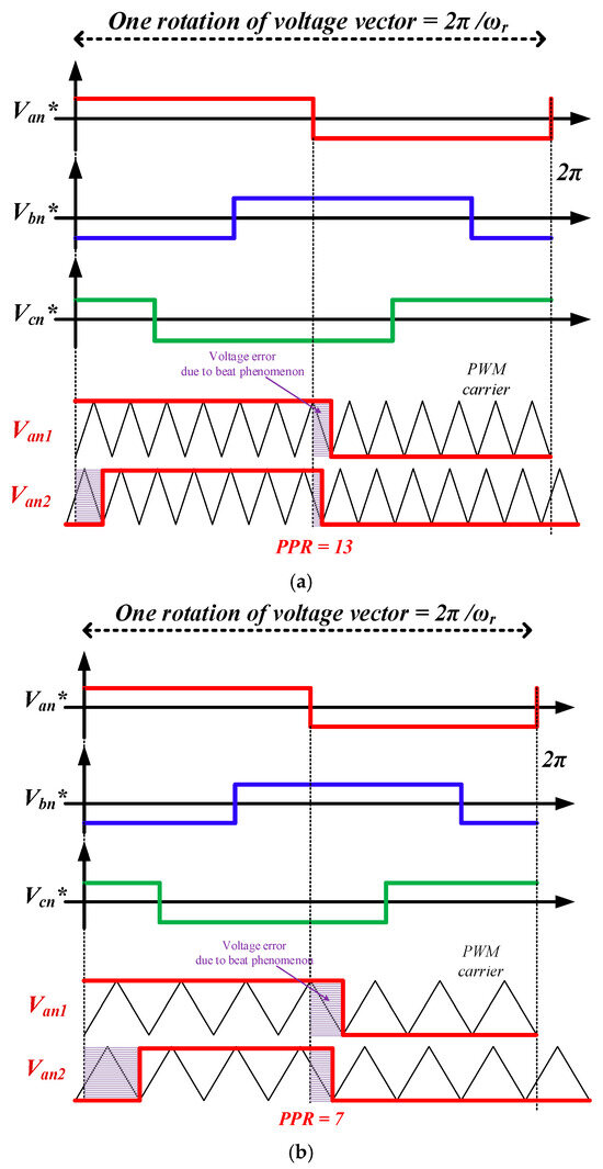
Figure 4.
Pole voltage error due to the beat phenomenon in 6-step operation. (a) PPR = 13, (b) PPR = 7.
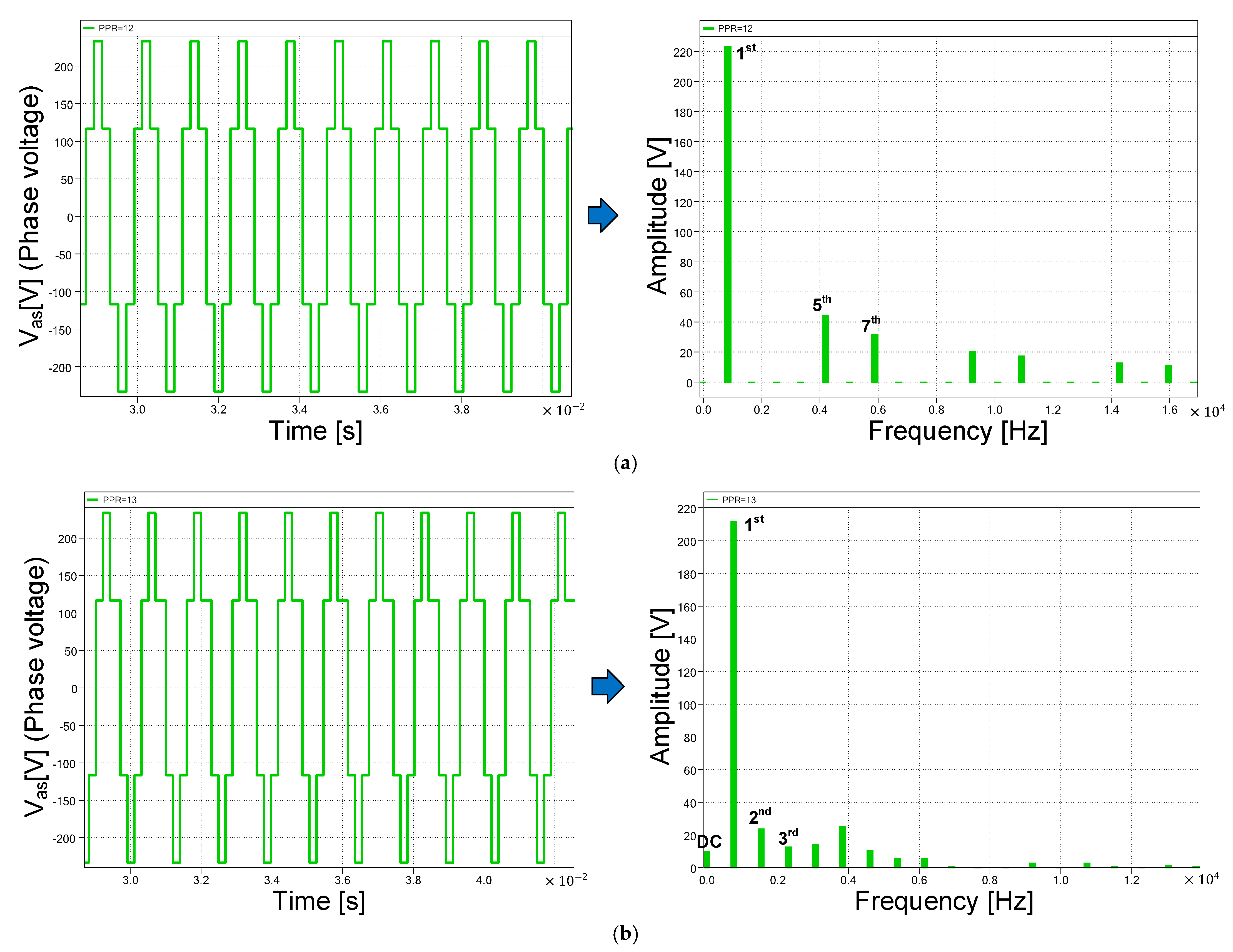
Figure 5 shows the FFT results of the phase voltage waveform in six-step operation when the PPR is set to 12 and 13, respectively. The inverter operating conditions are as shown in Table 1. In Figure 5a, as the synchronous PWM condition is satisfied (PPR = 6n), the frequency components of the phase voltage are composed of only odd harmonic components, excluding the DC component and the 3n harmonics. On the other hand, in Figure 5b, the beat phenomenon causes a voltage error, and the DC voltage component appears in the output for one cycle, as in Figure 4a. The DC voltage component and additional harmonic voltages, which did not occur in (a), are generated. The 3n harmonic voltage has no effect in three-phase motors with a neutral point shorted, and although other harmonic components are also generated, the most problematic one is the DC component frequency voltage. Since the impedance of the DC component is determined only by the resistance component of the motor, the DC voltage error induces an excessive current, which can lead to the high current ripple and torque ripple issues mentioned above.
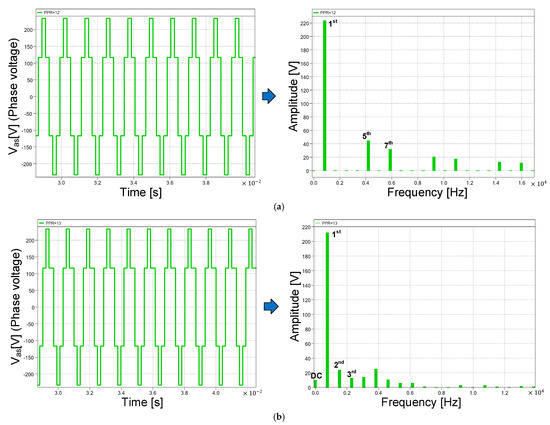
Figure 5.
Phase voltage waveforms and FFT results. (a) PPR = 12, (b) PPR = 13.

Table 1.
Parameters of inverter and motors.
3. Proposed Beatless Operation and Its Implementation in MCU Timer Module
In this chapter, the beatless operation method in the six-step operation area is proposed. This method operates based on a fixed inverter switching frequency and applies an up–down carrier-based PWM. This paper not only presents the principle of the proposed beatless method but also provides a specific timer logic configuration method that can be implemented based on an MCU for motor drive. For a detailed explanation, the basic register configuration method applied in the MCU timer module for a carrier-based PWM will be explained, followed by a detailed description of how to modify each register to implement the proposed beatless operation.
3.1. Register Configuration of MCU Timer Module for Carrier-Based PWM
In this section, the basic carrier-based PWM method is produced along with the settings required to implement it in an MCU-based digital circuit. The timer module is utilized to generate the PWM output through the MCU, and to output PWM using the timer function, the configuration of various registers is required. This study describes the PWM-related register settings in the motor control MCU using arbitrary names for explanation.
Carrier-based PWM can be implemented on the MCU through the configuration of the four registers presented in Table 2. Figure 6 shows the register settings for one phase and the PWM switching output.
Table 2.
MCU timer register configuration and operation description for carrier-based PWM.
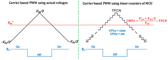
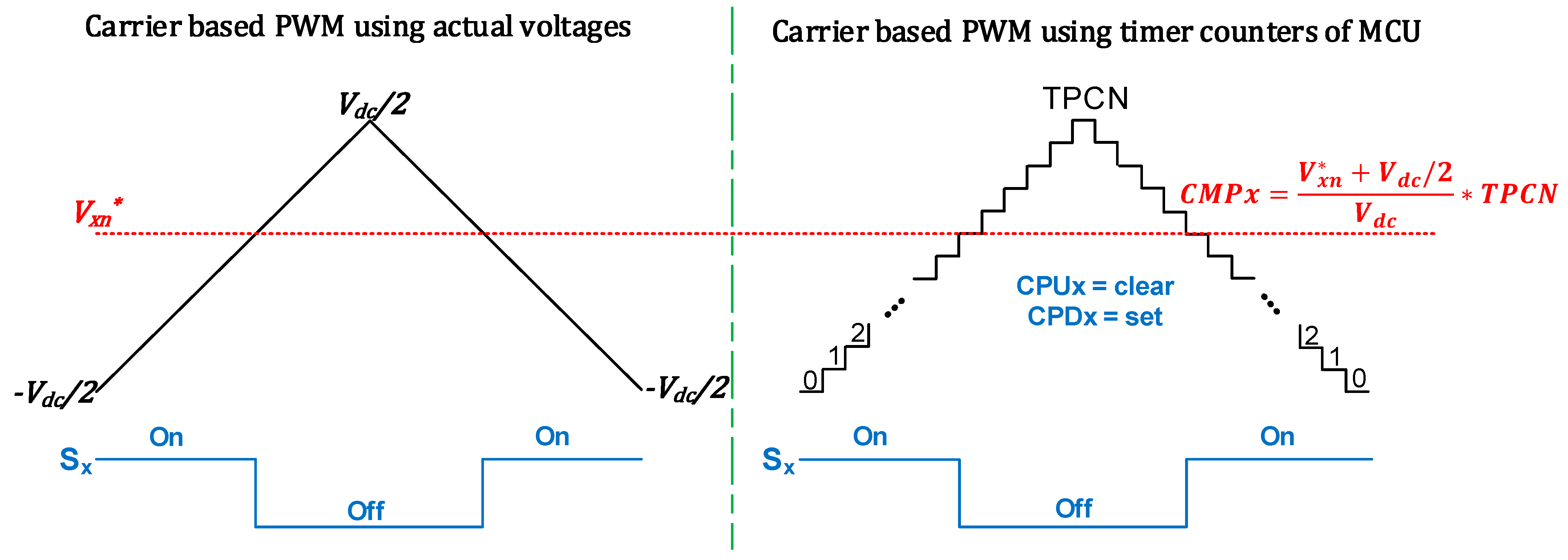
Figure 6.
Implementation of carrier-based PWM using the MCU’s timer registers.
In a typical carrier-based PWM, the maximum and minimum values of the carrier are determined by the pole voltage range of the inverter (−Vdc/2 ~ Vdc/2). The final pole voltage reference (Vxn*) is then compared, and the corresponding phase switch signal (Sx) for the upper switch of the inverter leg is generated. To implement this in the MCU, the timer register configurations presented in Table 2 are required. Firstly, TPCN is the peak value of the carrier, determined by the inverter’s switching frequency. TPCN can be set as a ratio value between the MCU’s timer clock frequency and the desired switching frequency (ωclock/ωsw). When a fixed switching frequency is applied, TPCN is set to a constant value. The comparison count value, CMPx, is determined according to the pole voltage reference for the corresponding phase and is calculated as follows.
Finally, the polarity of the PWM signal is determined by CPUx and CPDx, which are set to ‘clear’ and ‘set’, respectively, in an inverter system with an active-high gating circuit. As shown in Figure 6, the final PWM switching signal (Sx) is generated identically in both cases. Therefore, in the basic carrier-based PWM, only the CMPx value corresponding to the comparison-match counter value is modified according to the pole voltage reference in each switching cycle, while the remaining three values (TPCN, CPUx, CPDx) maintain fixed settings. However, as shown in Figure 4a,b, such carrier-based PWM configurations result in voltage errors due to beat phenomena when the PPR is not set to a multiple of 6n during six-step operation. The beatless control method to address it will be presented in the following sections.
3.2. Voltage Command Modification Method for 6-Step Operation
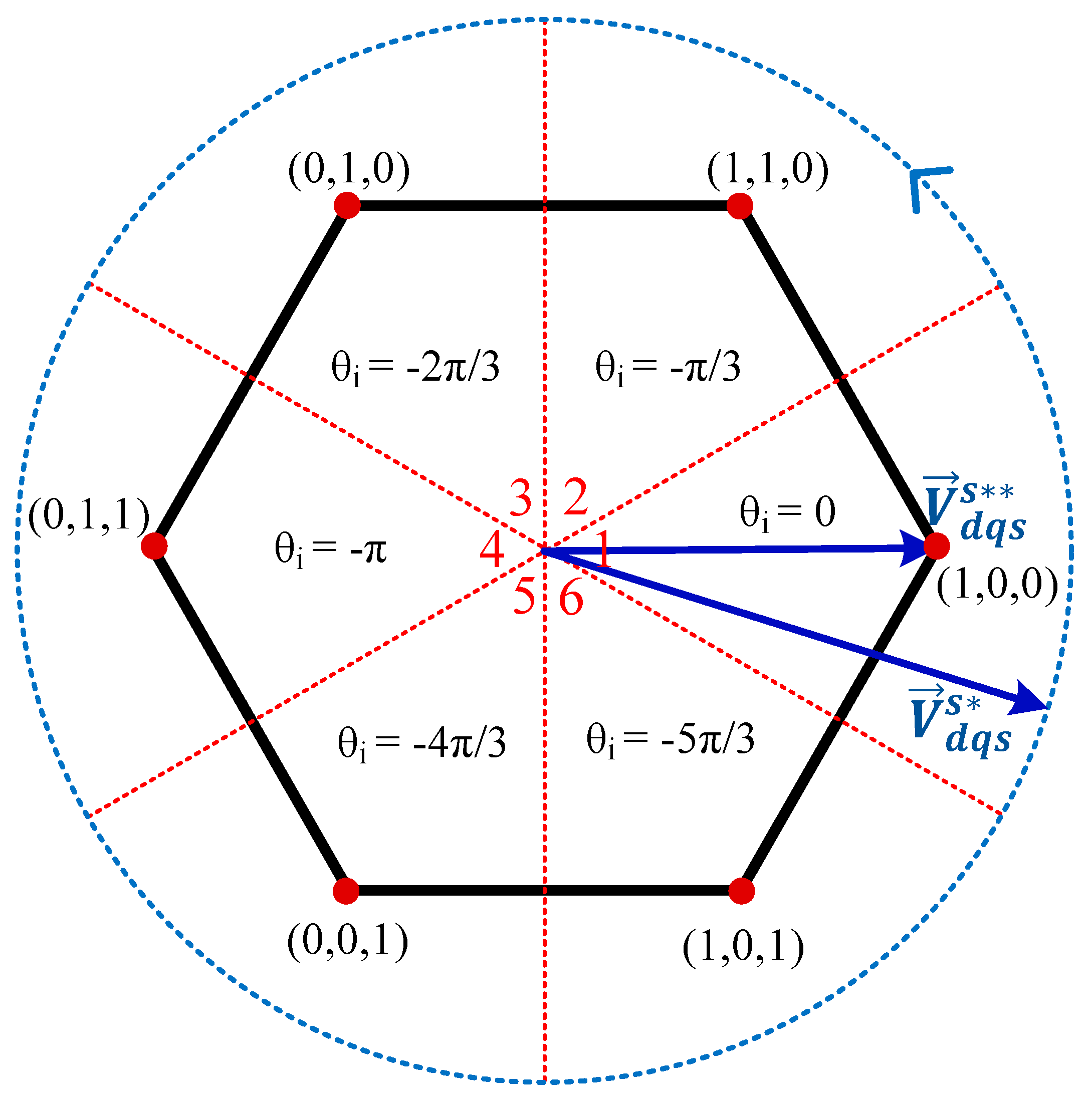
As the speed increases in three-phase inverter control for motor drive, the required modulation index (MI) also increases, causing the voltage vector to exceed the range of the voltage hexagon presented in Figure 2. Since it is not possible to output voltage vectors outside the voltage hexagon, the voltage reference vector must be corrected to be placed within the hexagon region or at the boundary line. This method is known as overmodulation (OVM), and various studies have proposed OVM methods for three-phase inverters. Some OVM methods allow the inverter’s operating range to transition from the linear modulation region to the six-step operation region. Since this paper focuses on the beat phenomenon in six-step operation, the detailed processes and performance of OVMs are not discussed. In the six-step operation region, as shown in Figure 7, the voltage reference vector () from the current controller rotates with a diameter larger than that of the voltage hexagon. The final output voltage vector is determined as the six vertex points indicated by red dots, and the voltage vector correction is performed based on its phase. In Figure 7, the region is divided into six areas, numbered 1 to 6, with a 60-degree interval. When the voltage command vector lies in a specific region, the voltage vector is corrected to the vertex vector within that region. The final voltage reference is denoted as , where ** indicates the corrected value by OVM.
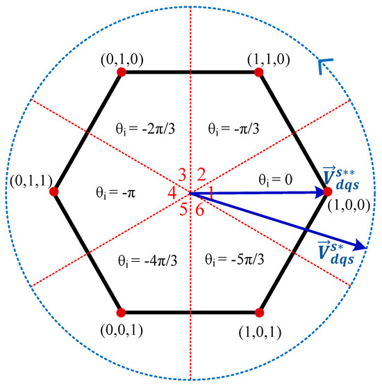
Figure 7.
Operating region setup and voltage reference modification method in 6-step operation region.
As mentioned above, in the six-step operation region, the final voltage reference vector is confined to the six vertices, and the corresponding pole voltage reference is set to either Vdc/2 or −Vdc/2, as shown in Figure 4a,b. This can also be confirmed through the conventional carrier-based PWM block diagram for six-step operation shown in Figure 8. When Vabcn* is set to either Vdc/2 or −Vdc/2, CMPx is set to either 0 or TPCN, respectively. In this case, no switching occurs, which means that all three phases are clamped during one switching cycle. Therefore, as shown in Figure 4a,b, switching only occurs at the peak or bottom points of the carrier. If the phase of the carrier does not align with the phase of the desired voltage vector, a voltage error will inevitably occur. To eliminate this voltage error phenomenon, an additional process is required to align the phase of the PWM signal with that of the initial voltage reference.
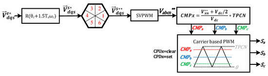
Figure 8.
Conventional carrier-based PWM method in 6-step region without beatless control.
3.3. Method for Determining Pole Voltage Considering Beatless
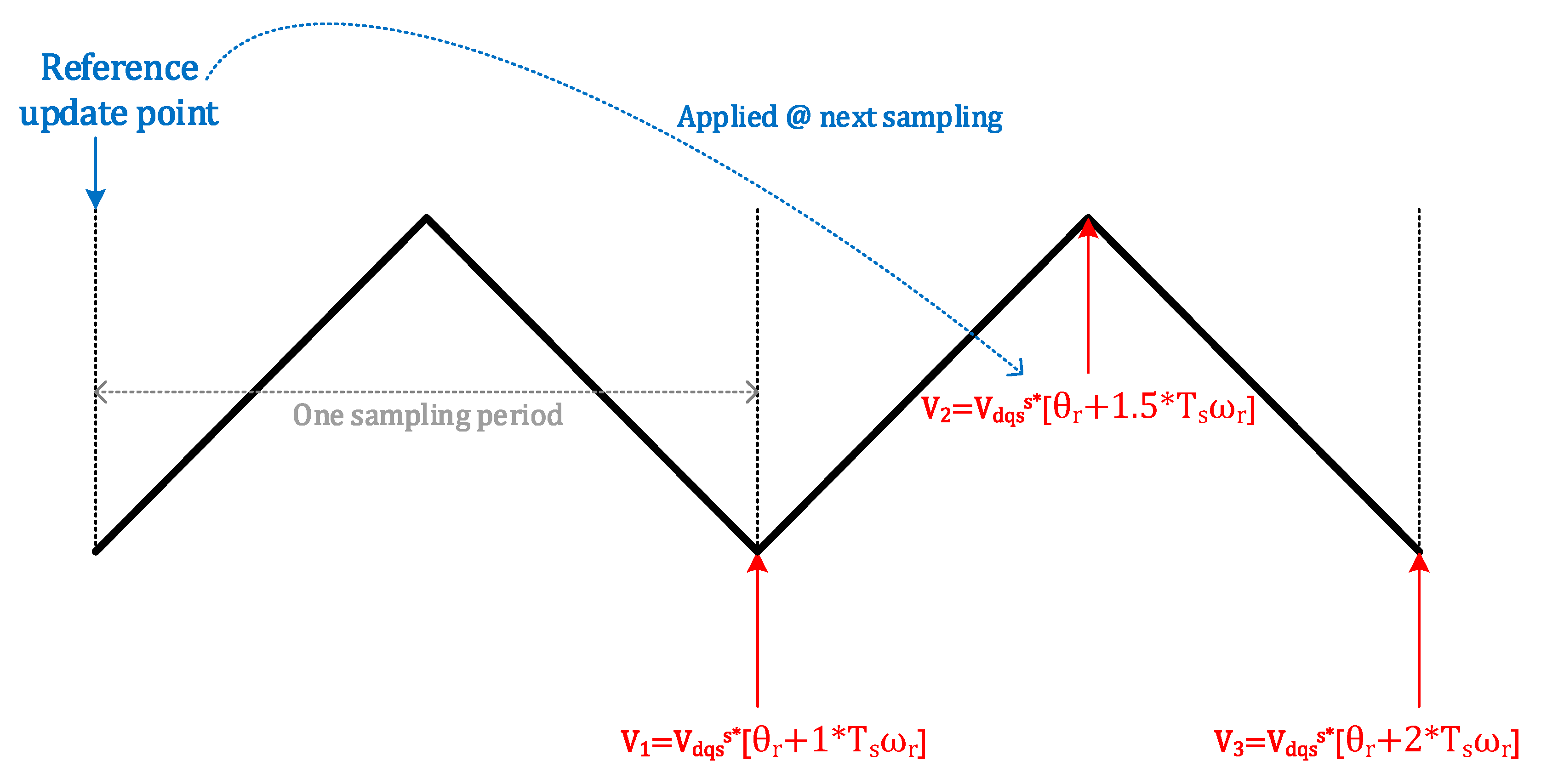
In motor drive systems applying digital control based on an MCU, the control logic is typically synchronized with the inverter’s switching frequency. When using carrier-based PWM, the calculations for the control operations are performed at the peak or valley of the carrier, and a new voltage reference is generated. This study assumed that the control calculation is executed and the voltage reference is updated at the valley point of the carrier. The calculated voltage reference cannot be applied immediately in the current sampling; instead, it is delayed by one sampling period and applied in the next sampling. To compensate for the voltage error caused by the sampling delay, the phase is advanced by 1.5 × ωr × Ts, where Ts is the sampling period. The compensation is carried out based on the next sampling’s mid-point.
In Figure 9, the point when the calculated voltage reference is actually applied is indicated based on the carrier. The compensation for the sampling delay in this digital control is also included in Figure 8. In high-speed operation regions such as the six-step operation, the motor’s position significantly changes within one sampling cycle, so the compensation of 1.5 × Ts is essential. In the same way, the voltage references at the beginning and end of the sampling cycle are calculated by reflecting the phase variation. Here, V1 is the voltage reference at the starting point, with a delay compensation of Ts, and V3 is the voltage reference at the end point, with a delay compensation of 2 × Ts. The switching timing for the proposed beatless control is determined based on these two voltage references (V1 and V3).
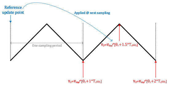
Figure 9.
Voltage references considering the phase variation at the peak and valley points of the PWM carrier.
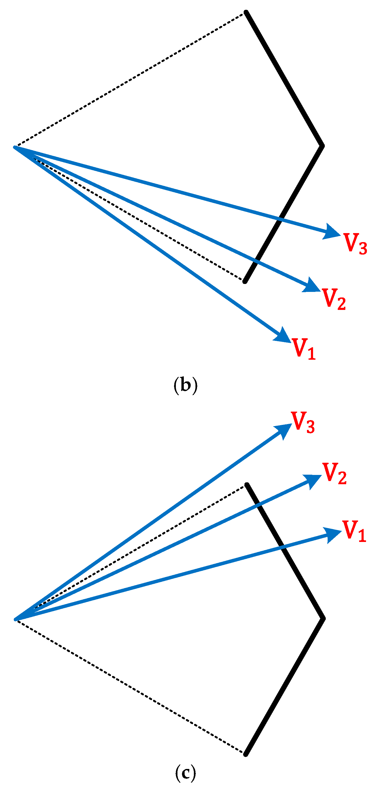
As shown in Figure 7, the six regions set on the voltage hexagon form a symmetric structure with 60-degree intervals. Therefore, through coordinate transformation, the voltage vectors in regions 2 to 6 are rotated to the first region. This rotating transformation can be written using the θi, which is presented in Figure 7, as follows.
Through the coordinate transformation in (4), always exists in the first region. The voltage placements of V1, V2, and V3 for are shown in Figure 10. Here, the reference region is set based on the V2 voltage vector, so the V2 vector is always placed in the first region.
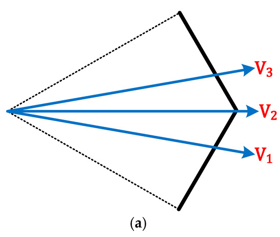
Figure 10.
Case determination based on the positions of V1, V2, and V3 vectors of vdqsi*. (a) Case I, (b) case II, (c) case III.
Figure 10a shows that all three voltage vectors are within the phase angle range of the first region, so in this case, the voltage vertex vector of the current region is maintained during the sampling period. As a result, no switching state changes occur, and the three pole voltage references are determined as follows.
Here, Sx_vertex refers to the switching states of the vertex voltage vector in the corresponding region. When V1, V2, and V3 are located within a single region, as shown in Figure 10a, this is referred to as Case I in this paper.
Next, Figure 10b corresponds to the case where the V1 vector is in the previous region, while V2 and V3 are in the current region. In this case, at the beginning of the switching period, the switching state is set as the vertex voltage vector of the previous region, and during the current sampling period, the switching state of one phase changes to output the vertex voltage vector of the current region. This situation is referred to as Case II. The pole voltage references in Case II are shown in Table 3. When switching occurs on one phase leg that does not have ±Vdc/2 as the pole voltage, it results in six possible combinations of phases being turned on or off. In Table 3, the pole voltage references are indicated for the possible six combinations based on the movement of the vertex voltage vector, and θ1, θ2, and θ3 represent the phase angles of V1, V2, and V3, respectively. Finally, Figure 10c represents the case where V1 and V2 are in the current region and V3 is in the next region. This is referred to as Case III, and the pole voltage references resulting from the region shift are also included in Table 3. Considering the nonlinearity of the inverter, such as dead time, the pole voltage presented in Table 3 can be adjusted based on the direction and magnitude of the current [18,19,20]. However, this adjustment applies only to the phase where switching occurs. As there is no switching in the clamped phase, pole voltage correction is unnecessary in that case.
Table 3.
Pole voltage calculation formula for 6-step beatless operation.
In the generation of these voltage commands, a case determination is required, which can be simply carried out based on the values of θ1 and θ3 as follows. In Case I, θ1 and θ3 satisfy the following condition.
In Case II, θ1 is determined as follows:
In Case III, θ1 is determined as follows:
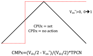
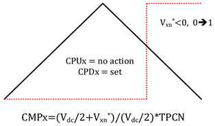
3.4. Proposed Beatless Control Method Based on Fixed Switching Frequency
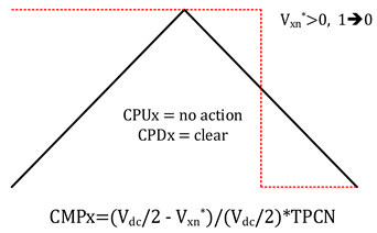
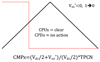
In the linear modulation region, the triangular carrier-based PWM involves both the off and on sequences for all phase legs in each switching cycle. In other words, all phase legs switch twice per cycle. However, in six-step operation, no switching event occurs or either an on sequence or off sequence is executed at one phase leg. In Case I, no switching event occurs, and the on or off sequence settings for Case II and III are shown in Table 2. For the proposed beatless operation, the method calculating the CMPx values and setting the CPUx and CPDx differ for each sequence. Table 4 summarizes the CMPx and polarity register settings according to the on/off sequence and the polarity of the pole voltage reference in Cases II and III. By applying this switching operation setting from Table 4 to only one phase leg, the other two phase legs maintain the switching states without switching operation. In Case I, no switching occurs, so both CPUx and CDUx are set to no action, and the CMPx value has no effect on the operation.
Table 4.
Setup of polarity and comparison-match registers (CPUx, CPDx, CMPx) for implementing a single switching operation in the proposed 6-step beatless control.
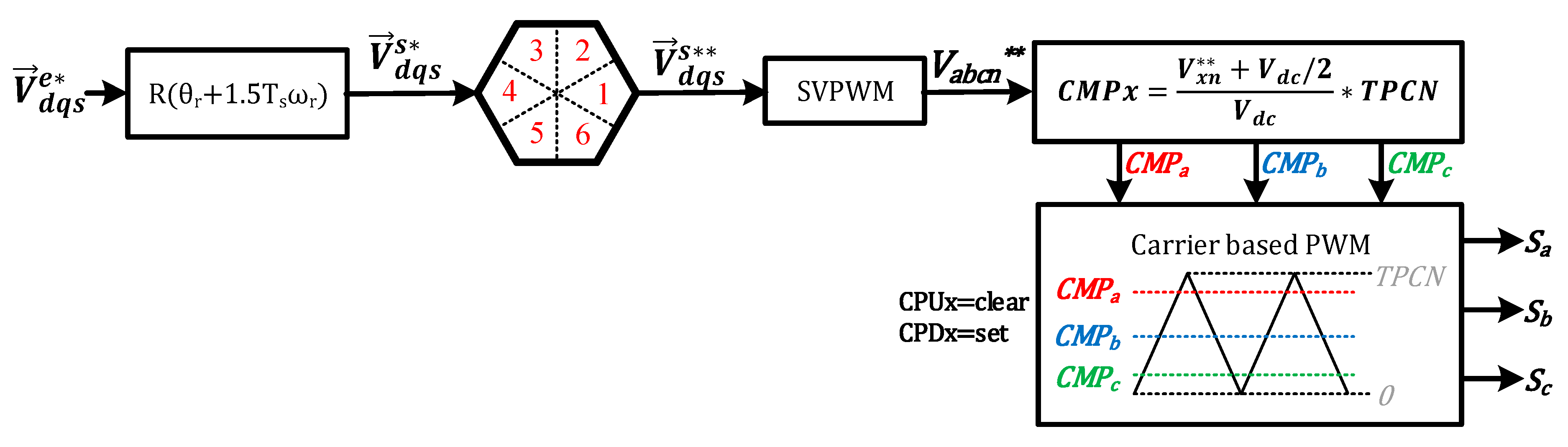
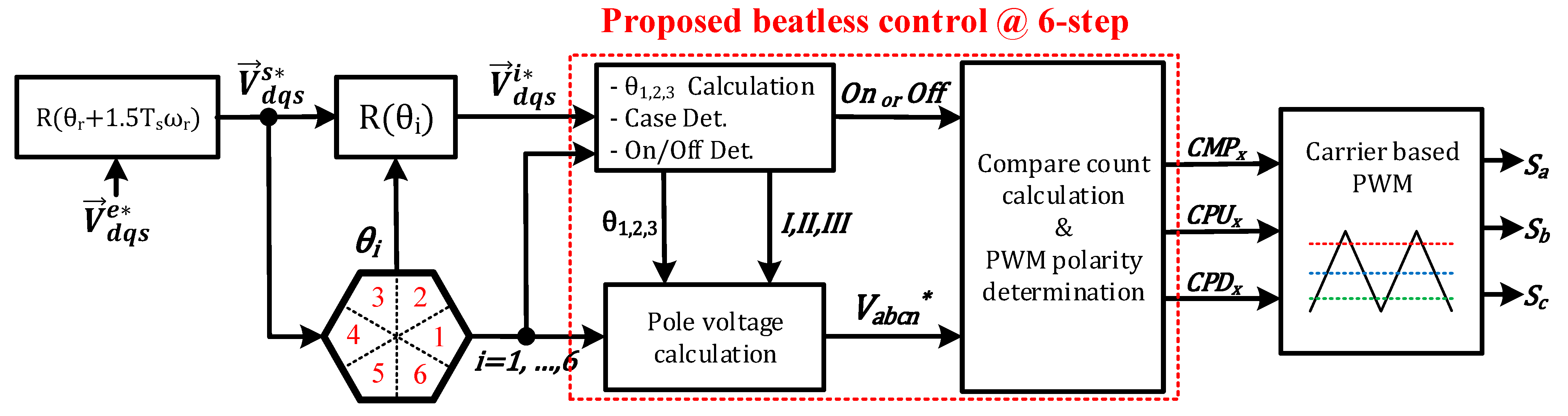
Figure 11 is a block diagram for the proposed beatless control in the six-step operation. Based on Figure 7, the region of the initial voltage reference vector is set, and the voltage vector is coordinate-transformed to the first region. ‘Case’ and ‘on/off sequence’ are then determined based on this, and the pole voltage reference is calculated according to Table 3. Based on the calculated pole voltage reference and the determined on/off sequence, the PWM registers of CPUx, CPDx, and CMPx are decided and applied to the conventional PWM logic. The proposed six-step beatless control method can be applied to most general motor control MCUs and is feasible even for low-cost MCUs where a variable switching frequency modulation is impossible, as it is implemented in the fixed switching frequency state.
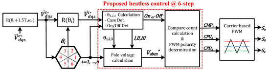
Figure 11.
Entire block diagram of the proposed 6-step beatless control.
4. Verification of the Proposed Beatless Control Through the Real-Time Simulator
In this study, a real-time simulator, Typhoon HIL, is used to validate the feasibility and operational performance of the proposed beatless control method. Figure 12 shows the experimental setup including the real-time simulator. The proposed beatless algorithm is implemented on the TMS320F28335, the MCU for motor control, which generates the PWM signals. The generated PWM signals are input into the HIL device to evaluate the motor drive performance. An interface board is designed between the HIL device and the MCU, allowing the PWM signals from the MCU to be fed into the HIL device and the current and voltage analog signals generated by the HIL device to be acquired via the MCU’s ADC. This corresponds to a configuration identical to the actual experimental environment. Additionally, the ABZ pulse information of an encoder is generated by the HIL and acquired by the MCU to detect the rotational position of the permanent magnet motor. In this simulation setup, the motor’s current and torque output can be monitored through dedicated HIL software, and the internal variables used for control can be checked via an oscilloscope through the MCU’s DAC.
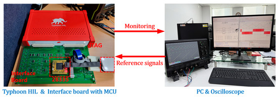
Figure 12.
Experimental setup including the real-time simulator (Typhoon HIL) and the MCU (TMS320F28335).
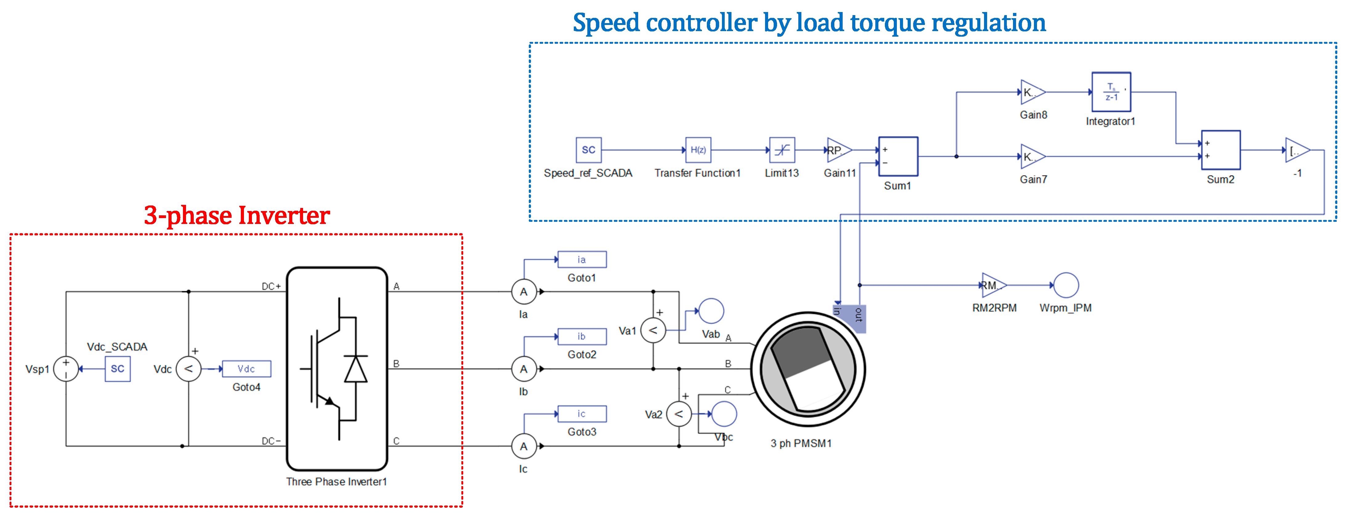
Figure 13 represents the circuit created in the real-time simulator. The target motor operates in torque control mode and the load torque is set to control the rotating speed. This setup is the same as the one used to verify the motor’s torque control performance in a typical dynamometer test environment. The parameters of the permanent magnet synchronous motor and inverter used in the simulation are listed in Table 1.
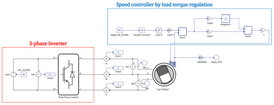
Figure 13.
Circuit configuration for real-time simulation and speed setting method.
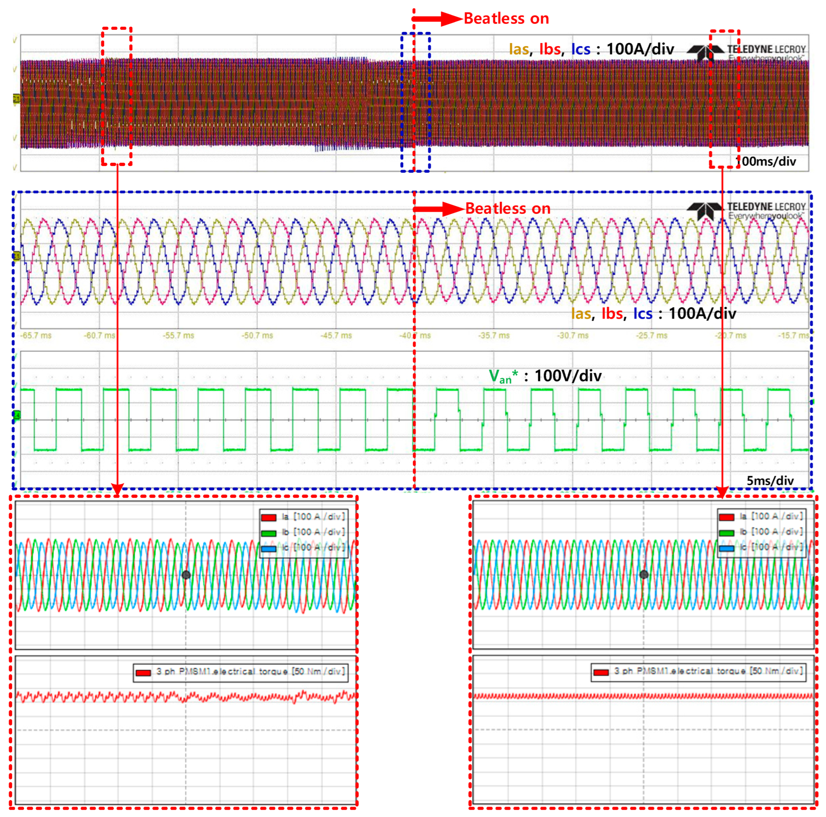
Figure 14 shows the waveforms of the phase current, phase-a pole voltage reference, and torque output when the speed is set to 5500 [r/min] and the motor torque output is set to maximum. With the speed setup beyond the rated speed, the flux weakening operation is applied, and the torque output is set to a lower value compared to the rated torque. In the region before the mid-point where beatless control is not applied, the operation is limited to Case I regions, resulting in the pole voltage references being set to only ±Vdc/2. With a PPR of about 27.27, voltage errors due to the beat phenomenon occur, and as a result, a current ripple of low frequency is observed. As analyzed in Figure 5 above, it is expected that the DC component voltage error occurs, which causes a current error, and then it interacts with the current controller, increasing the peak value of the three-phase current, resulting in the ripple of low frequency. Additionally, at the torque output, the low-frequency ripple components are added beside the 6th-harmonics torque ripple due to the six-step operation. On the other hand, after the proposed beatless control method is applied, the phase-a pole voltage not only has ±Vdc/2 but also has intermediate values at the switching points where the polarity changes. This corresponds to the pole voltage reference of the corresponding phase, reflecting the phase of the initial voltage vector reference as specified in Table 3. Through this, six-step operation considering the initial voltage reference phase is applied, and it is confirmed that the low-frequency ripple components in the current and torque are eliminated. The low-frequency ripple components are caused by the interaction between the DC component of the voltage output due to the beat voltage presented in Figure 5b and the current controller. In the stator reference frame, the DC component current appears as a fundamental harmonic AC component in the synchronous reference frame, which results in various ripple components in the voltage output of the current controller depending on the rotating speed and the bandwidth setting of the current controller. To verify this, the results at higher speeds are presented below.
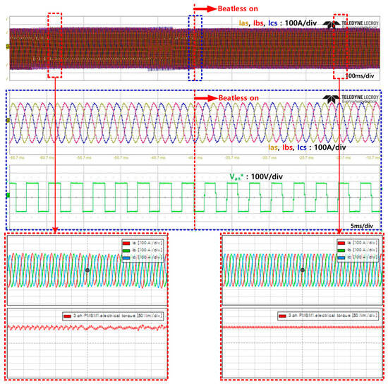
Figure 14.
(Real-time) Simulation results at 5500 [r/min] and 120 [Nm]: results before and after applying the proposed beatless control.
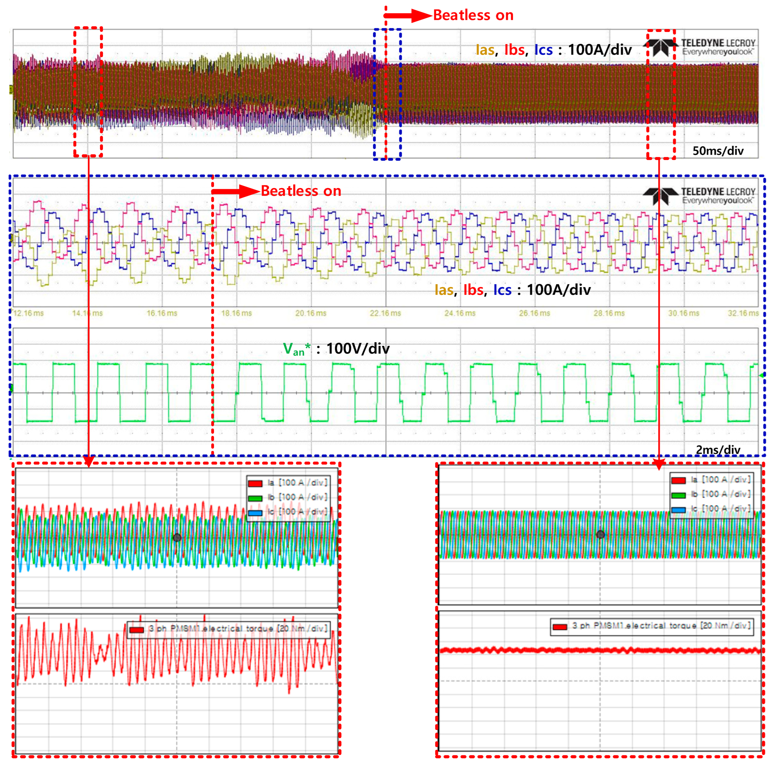
In Figure 15, under the same operating conditions as Figure 14, the motor speed is only changed to the maximum speed of 12,000 [r/min], which corresponds to PPR = 12.5. In the section before the beatless control is applied, the current and torque ripples occur due to the beat phenomenon, and the degree of the ripple is confirmed to be much more severe compared to Figure 14 (PPR = 27.27). As mentioned above, as the rotating speed increases and the PPR decreases, the side effects of the beat phenomenon become more pronounced. Also, it can be observed that the frequency of the ripple has significantly increased. This is because, as the rotational speed increases, the error of the DC component in the stator reference frame generates an error in the fundamental harmonic component in the synchronous reference frame control. The frequency of this fundamental harmonic component has increased as a result. After the proposed beatless control is applied, the pole voltage takes intermediate values between ±Vdc/2 at the switching points, confirming that six-step operation, reflecting a phase of the voltage reference, is applied. As a result, low-frequency ripples in both the current and torque are almost perfectly eliminated.
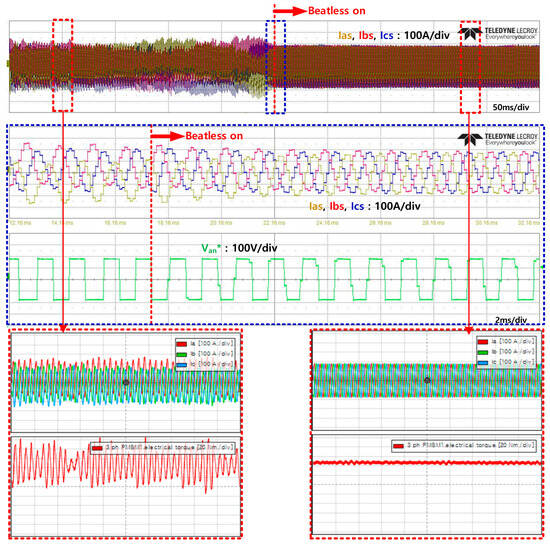
Figure 15.
(Real-time) Simulation results at 12,000 [r/min] and 45 [Nm]: results before and after applying the proposed beatless control.
5. Conclusions
This study presents a beatless six-step operation method for a three-phase motor drive system with a fixed switching frequency, and its performance was verified through a real-time simulator. Conventional research on six-step beatless control has either applied a synchronized PWM method or merely proposed beatless concepts. However, this study presents a detailed approach that can be applied to carrier-based PWM, including specific settings for the MCU timer registers. The proposed beatless method does not simply set the pole voltage reference to ±Vdc/2 for six-step operation but adjusts the pole voltage reference considering the phase of the initial voltage reference vector. Additionally, in the PWM using an up–down carrier, the registers determining the PWM polarity for the carrier’s rising and falling intervals are changed at each switching period to precisely match the phase of the voltage reference vector. The proposed method can be implemented through most motor control MCUs as it only requires adjusting the fixed switching frequency and PWM-related register settings. As a result, the DC component voltage error in the six-step voltage output is completely eliminated. The proposed beatless control method was implemented on an MCU linked to a real-time simulator, and its operational performance was specifically verified.
Funding
This research received no external funding.
Data Availability Statement
Data are contained within the article.
Conflicts of Interest
The author declares no conflict of interest.
References
- Atanalian, S.; Sebaaly, F.; Zgheib, R.; AL-Haddad, K. Real-Time Implementation of Three-Phase Z Packed U-Cell Modualr Multilevel Grid-Connected Converter Using CPU and FPGA. Electronics 2024, 13, 2186. [Google Scholar] [CrossRef]
- Sang, Z.; Li, S.; Huang, Y.; Gao, X.; Qiao, R. Indirect Matrix Converter Hardware-in-the Loop Semi-Physical Simulation Based on Latency-Free Decoupling. Electronics 2023, 12, 4802. [Google Scholar] [CrossRef]
- Shanyeghan, M.; Benedetto, M.D.; Lidozzi, A.; Solero, L. HIL-Based Fault-Tolerant Vector Space Decomposition Control for a Six-Phase PMSM Fed by a Five-Level CHB Converter. Energies 2025, 18, 507. [Google Scholar] [CrossRef]
- Sonzanski, K. Low-Cost Hardware Analog and Digital Real-Time Circuit Simulators for Developing Power Electronics Control Circuits. Energies 2024, 17, 6359. [Google Scholar] [CrossRef]
- Holtz, J.; Lotzkat, W.; Khambadkone, A.M. On continuous control of PWM inverters in the overmodulation range including the six-step mode. IEEE Trans. Power Electron. 1993, 8, 546–553. [Google Scholar] [CrossRef]
- Lee, K.; Han, Y. PWM strategy in OVM and Six-Step Regions for Open-End Winding PMSM Fed by a Dual Inverter with a Common DC Bus. IEEE Trans. Power Electron. 2024, 39, 13696–13707. [Google Scholar] [CrossRef]
- Wang, B.; Wang, L.; Yu, Y.; Xu, D. Adaptive Overmodulation Strategy for PMSM Field-Weakening Control Based on Working Quadrant. IEEE Trans. Ind. Electron. 2023, 70, 9959–9970. [Google Scholar] [CrossRef]
- Jung, B.; Lee, T.; Nam, K. Overmodulation Strategy for Voltage Source Inverter With a Single DC-Link Current Sensor. IEEE Trans. Ind. Appl. 2022, 58, 531–540. [Google Scholar] [CrossRef]
- Chen, Z.; Mao, H.; Yang, X.; Wang, Z. A study on pulse width errors of digitized naturally sampled PWM. In Proceedings of the 2008 IEEE Power Electronics Specialists Conference, Rhodes, Greece, 15–19 June 2008; pp. 592–597. [Google Scholar] [CrossRef]
- Stumpf, P.; Jardan, R.K.; Nagy, I. Comparison of naturally sampled PWM techniques in ultrahigh speed drives. In Proceedings of the 2012 IEEE International Symposium on Industrial Electronics, Hangzhou, China, 28–31 May 2012; pp. 246–251. [Google Scholar] [CrossRef]
- Stumpf, P.; Jardan, R.K.; Nagy, I. Subharmonics generated by space vector modulation in ultrahigh speed drives. IEEE Trans. Ind. Electron. 2012, 59, 1029–1037. [Google Scholar] [CrossRef]
- Halasz, S. DC components and subharmonics of carrier-based PWM. In Proceedings of the 2012 15th International Power Electronics and Motion Control Conference (EPE/PEMC), Novi Sad, Serbia, 4–6 September 2012. [Google Scholar] [CrossRef]
- Jardan, R.K.; Stumpf, P.; Bartal, P.; Varga, Z.; Nagy, I. A novel approach in studying the effects of subharmonics on ultrahigh-speed AC motor drives. IEEE Trans. Ind. Electron. 2011, 58, 1274–1281. [Google Scholar] [CrossRef]
- Ke, Z.; Zhang, J.; Raich, R. Low-Frequency Current Oscillation Reduction for Six-Step Operation of Three-Phase Inverters. IEEE Trans. Power Electron. 2017, 32, 2948–2956. [Google Scholar] [CrossRef]
- Hara, T.; Taniguchi, S.; Ajima, T.; Sawahata, M.; Hori, M.; Tsukagoshi, T. Synchronous PWM Control with Carrier Wave Phase Shifts for Permanent Magnet Synchronous Motor. IEEE Trans. Ind. Appl. 2022, 58, 5650–5658. [Google Scholar] [CrossRef]
- Hara, T.; Taniguchi, S.; Ajima, T.; Sawahata, M.; Hori, M.; Tsukagoshi, T. Vibration and Loss Reduction of Permanent Magnet Synchronous Motor Driven by Synchronous PWM Control with Carrier Wave Phase Shifts. In Proceedings of the 2021 IEEE Energy Conversion Congress and Exposition (ECCE), Vancouver, BC, Canada, 10–14 October 2021. [Google Scholar] [CrossRef]
- Tommaso, A.; Miceli, R.; Nevoloso, C.; Marsala, S. Practical Implementation of a Synchronous PWM Strategy for Low Switching Frequency FOC of IM Drives with ATSAM3X8E Microcontroller. In Proceedings of the 2021 Sixteenth International Conference on Ecological Vehicles and Renewable Energies (EVER), Monte-Carlo, Monaco, 5–7 May 2021. [Google Scholar] [CrossRef]
- Lin, H.; Cai, C.; Chen, J.; Gao, Y.; Vazquez, S.; Li, Y. Modulation and Control Independent Dead-Zone Compensation for H-Bridge Converters: A Simplified Digital Logic Scheme. IEEE Trans. Ind. Electron. 2024, 71, 15239–15244. [Google Scholar] [CrossRef]
- Wang, H.; Xu, J.; Ye, J.; Li, B.; Huang, S.; Huang, Y.; Liu, D.; Shen, A. Harmonic spectra analysis of digital SPWM in VSI with DC bus ripple and dead-time effects. IEEE Trans. Power Electron. 2023, 38, 9494–9513. [Google Scholar] [CrossRef]
- Lin, Y.; Lai, Y. Dead-time elimination of PWM-Controlled inverter/converter without separate power sources for current polarity detection circuit. IEEE Trans. Ind. Electron. 2009, 56, 2121–2127. [Google Scholar]


Disclaimer/Publisher’s Note: The statements, opinions and data contained in all publications are solely those of the individual author(s) and contributor(s) and not of MDPI and/or the editor(s). MDPI and/or the editor(s) disclaim responsibility for any injury to people or property resulting from any ideas, methods, instructions or products referred to in the content. |
© 2025 by the author. Licensee MDPI, Basel, Switzerland. This article is an open access article distributed under the terms and conditions of the Creative Commons Attribution (CC BY) license (https://creativecommons.org/licenses/by/4.0/).