Article

Wet Etching-Based WO3 Patterning for High-Performance Neuromorphic Electrochemical Transistors

by
Liwei Zhang
1,
Sixing Chen
1,
Shaoming Fu
1,
Songjia Han
2,
Li Zhang
1,3,
Yu Zhang
1,
Mengye Wang
3,
Chuan Liu
1 and
Xiaoci Liang
1,*
1
The State Key Laboratory of Optoelectronic Materials and Technologies, Guangdong Province Key Laboratory of Display Material and Technology, School of Electronics and Information Technology, Sun Yat-Sen University, Guangzhou 510275, China
2
College of Electronic Engineering, College of Artificial Intelligence, South China Agricultural University, Guangzhou 510642, China
3
School of Materials, Sun Yat-Sen University, Shenzhen 518107, China
*
Author to whom correspondence should be addressed.
Electronics 2025, 14(6), 1183; https://doi.org/10.3390/electronics14061183
Submission received: 25 February 2025 / Revised: 16 March 2025 / Accepted: 17 March 2025 / Published: 18 March 2025
(This article belongs to the Section Electronic Materials, Devices and Applications)

Abstract

:
WO3-based electrochemical transistors (ECTs) are recognized as candidates for three-terminal memristors due to their high on–off ratio, long retention time, and rapid switching speed. However, their patterned fabrication often relies on complex vacuum systems or extreme processing conditions, hindering cost-effective scalability. Here, we developed a novel wet etching technique integrated with sol–gel-derived WO3 channels, enabling ambient-air fabrication of Nafion-WO3 ECTs. The wet-etched devices achieve an on–off ratio of ~105, surpassing unetched and dry-etched counterparts by orders of magnitude. Furthermore, they exhibit exceptional paired-pulse facilitation and long-term stability, maintaining 12 distinct conductance states for 103 s, and an on–off ratio of ~102 over 25 read–write cycles. XPS result shows higher W5+ content and M-O-H bond proportion for wet-etched devices, revealing an optimized interface, with enhanced H+ injection efficiency. The simulated artificial neural network using this wet-etched ECT shows ~97% recognition accuracy for handwritten numerals. This approach offers a novel patterning strategy for developing cost-effective, high-performance neuromorphic devices.

1. Introduction

Neuromorphic computing, leveraging physical neural networks, has emerged as a next-generation paradigm to enable machine learning applications such as natural language processing and computer vision [1,2]. While traditional von Neumann architectures can simulate neural networks, their inherent separation of memory and processing units restricts data transfer speeds and hampers efficient large-scale data processing, particularly for complex neuromorphic algorithms [3]. In contrast, biological brains integrate computation and storage, achieving high efficiency and low power consumption—a feature inspiring efforts to overcome von Neumann bottlenecks. To mimic such biological synergy, researchers have developed diverse synaptic devices, including resistive random-access memory (ReRAM) [4,5], phase-change memory (PCM) [6,7], ferroelectric random-access memory (FeRAM) [8,9], and electrochemical random-access memory (ECRAM) [10,11].
Electrochemical transistors (ECTs), a key class of electrochemical random-access memory (ECRAM), function as three-terminal memristors governed by electrochemical ion doping. By modulating the gate voltage or current, ions in the electrolyte layer are controlled, enabling precise tuning of channel conductance. ECTs offer distinct advantages, including decoupled read/write operations and multi-state programmability [12]. Common doping ions—Li⁺ [13,14], Na⁺ [15], and H⁺ [16,17]—vary in performance. Protons (H⁺), with minimal ionic radius and mass, enable rapid transport and reduced structural degradation during doping. Nafion, a proton-conducting polymer electrolyte (>102 S cm⁻1 ionic conductivity), can enhance ECT response speed and durability due to its stability under harsh conditions [10,18]. For channel materials, transition metal oxides (TMOs) such as MoO3 [19], Nb2O5 [20], TiO2 [21], and WO3 [22] are widely explored. WO3, a wide-bandgap semiconductor (2.8–3.2 eV) [23], exhibits a layered structure and active d-orbitals that facilitate proton insertion at [WO6] octahedral sites under bias. This process injects electrons into the conduction band, significantly boosting channel conductivity and enabling high conduction on–off ratios [24,25].
Despite its widespread use in high-performance memory devices [26], WO3 lacks a simple, low-cost method for patterned fabrication, which limits the fabrication of large-area arrays for the application of artificial neural networks (ANN). Current approaches include shadow mask-assisted RF sputtering to confine deposition areas [18], reactive RF magnetron sputtering combined with photolithography and SF6-based reactive ion etching (RIE) [27], high-temperature (>100 °C) thermal atomic layer etching (ALE) using sequential boron trichloride (BCl3) and hydrogen fluoride (HF) treatments [28], and direct hydrothermal synthesis under high-temperature and atmospheric-pressure conditions with p-nitrobenzoic acid additives [29]. These methods require complex vacuum systems or extreme processing environments, posing challenges for safe, scalable, and economical ECT production. Therefore, exploring a new green and safe etching process to replace the traditional dry etching process with high hazard and power consumption is the purpose of this work.
In this study, we present a wet etching technique for WO3 patterning that integrates seamlessly with conventional photolithography, enabling ambient-air fabrication of channel structures. By combining this method with sol–gel-derived WO3 and a Nafion electrolyte, we demonstrate an ECT with exceptional storage performance, including high on–off ratios and prolonged retention times. By using experimental data of updatable conductance, we simulated an ANN based on the lookup table method with high accuracy in recognizing images. In Section 3.1, we compare the performance of wet etching, dry etching, and no etching on the WO3 film. In Section 3.2, we present the performance of wet etching WO3 devices on long-term and short-term memory. In Section 3.3, we present the implementation of the simulated ANN. This work may provide the solution for the patterning and integration of tungsten-based oxide on circuits in future work.

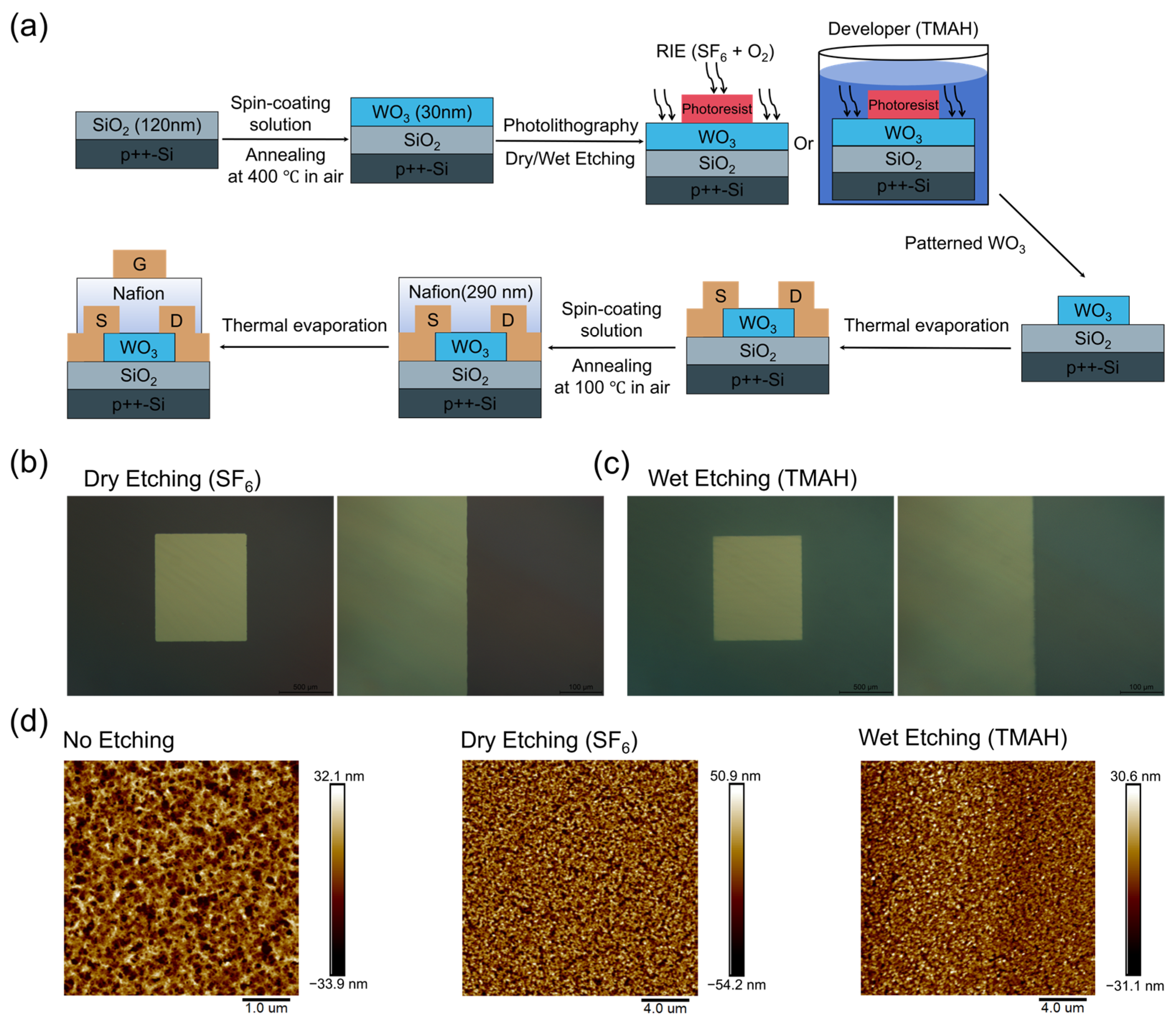
2. Materials and Methods

Tungsten hexachloride (WCl6, Aladdin, Shanghai, China) was dissolved in 99% absolute alcohol (Aladdin, Shanghai, China), and 0.1 mol/L precursor solution of WCl6 was prepared. The precursor solution of Nafion electrolyte was synthesized by mixing Nafion117 (Macklin, Shanghai, China) and 99% isopropanol (Aladdin, Shanghai, China) according to a volume ratio of 1:1. The WCl6 precursor solution was spin-coated on p++Si/SiO2 at 4000 rpm/30 s, and then annealed at 200 °C for 10 min and 400 °C for 1 h in air, thus obtaining the 30 nm WO3 thin film. Photolithography was employed to define channel patterns, followed by wet or dry etching.
Wet etching: Samples were developed using an alkaline positive photoresist developer (RZX-3038, Suzhou, China), primarily composed of tetramethylammonium hydroxide (TMAH). After development, the substrate was immersed in TMAH for 2 h under ambient conditions and rinsed with deionized water. The electricity power consumption is estimated at about 0.6 kW h.
Dry etching: Reactive ion etching (RIE, E100, Tailong Electronics, Beijing, China) was performed using SF6 and O2 (100 sccm each) at 100 W PolePower for 35 s, with a HighValvePOS of 30. The electricity power consumption is estimated at about 7.5 kW h for the total operation time (~1.5 h) of the equipment. Note that SF6 is an asphyxiant and greenhouse gas, which needs strict management, and its leakage may have an impact on the environment.
Following etching, residual photoresist was removed by sequential ultrasonic cleaning in acetone and ethanol (10 min each). A 60 nm aluminum (Al) source/drain electrode was deposited via thermal evaporation. The Nafion electrolyte precursor was spin-coated onto the sample at 2000 rpm for 30 s and annealed at 100 °C for 10 min. This process was repeated four times to achieve a 290 nm-thick electrolyte layer. Finally, a 100 nm Al gate electrode was thermally evaporated. Metal masks defined the patterns for source, drain, and gate electrodes, with channel dimensions of L = 200 μm and W = 1000 μm. X-ray photoelectron spectroscopy (XPS, Thermo K-Alpha, Guangzhou, China) was employed to analyze elemental composition changes during etching electrochemical doping. An atomic force microscope (AFM, Dimension Icon, Guangzhou, China) was used to analyze the WO3 surface morphology of ECTs without etching and with dry etching and wet etching. The thickness of Nafion and WO3 were both measured by AFM.

3. Results

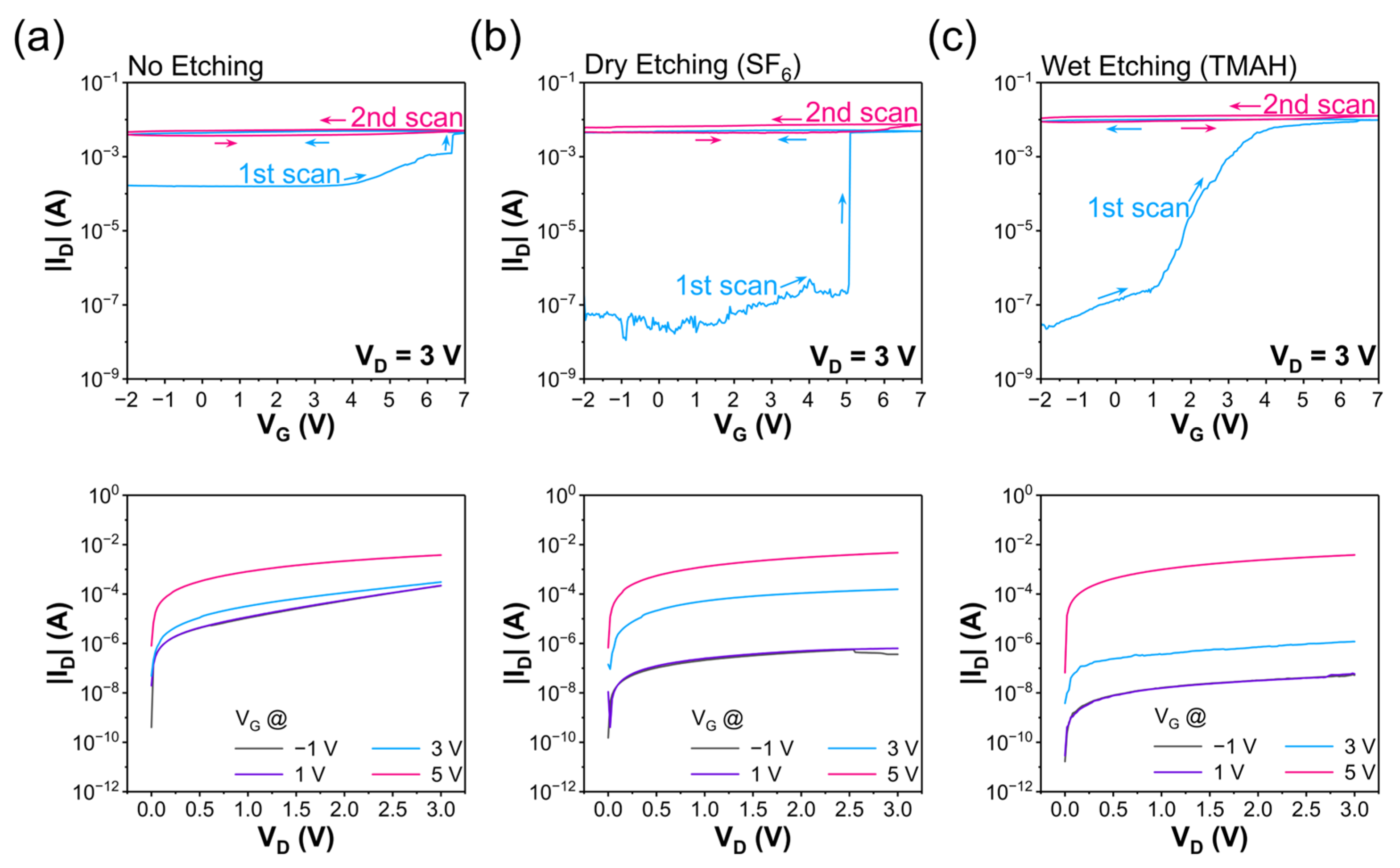
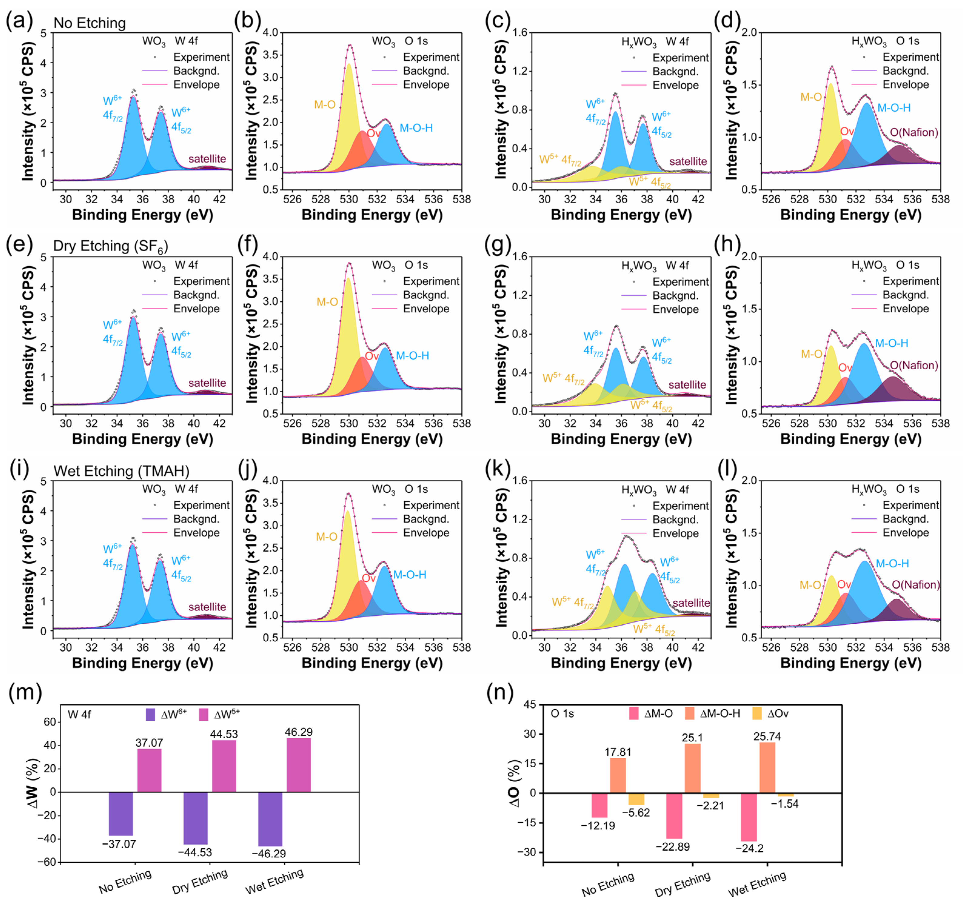
3.1. Comparison of Different Etching Methods

Figure 1a illustrates the fabrication process of the Nafion–WO3 ECT, integrating sol–gel synthesis, photolithography, etching, and thermal evaporation. The device adopts a top-gate top-contact structure, with WO3 as the channel layer and Nafion as the proton-conducting electrolyte. Figure 1b,c presents optical micrographs of patterned WO3 channels etched via SF6-based dry etching and TMAH wet etching, respectively. Both methods produced well-defined edges with negligible residual WO3 outside the target regions, confirming the precision and compatibility of the etching processes. Figure 1d shows the AFM images of the WO3 surface of the ECTs without etching and with dry etching and wet etching. Note that, compared with the pristine WO3 surface without etching, the surface of the etched WO3 is different from that of the pristine state because of the additional process. The root mean squares (RMS) of the roughness are 10.6 nm, 16.4 nm, and 8.45 nm for the non-etching, dry-etching, and wet-etching films, respectively. It is found that the film with the dry etching process is rougher than that with wet etching. This is likely because the ion bombardment caused damage to the film underneath the photoresist. The thickness of the WO3 film is about 30 nm without significant change after dry etching and wet etching, confirmed by the AFM.
Figure 2 presents the transfer and output characteristics of ECTs fabricated without etching and with different etching methods at VD = 3 V. All transfer curves exhibit counterclockwise hysteresis, indicating non-volatile conductance enhancement during the first voltage sweep, which persists in subsequent scans. The switching dynamic range ∆ID(on/off), defined as the ratio of ID(on) to ID(off) at VG = −2 V, reached 2.775 × 10⁵ for wet-etched devices—over 1000× and 2× higher than unetched (23.44) and dry-etched (1.153 × 10⁵) devices, respectively. Similarly, output curves demonstrated non-volatile ID modulation with increasing VG. At low VG (<1 V), all curves almost overlapped, reflecting a stable low-conductance state. For VG ≥ 3 V, ID surged irreversibly, confirming a switch to the high-conductance state. The saturation dynamic range ∆ID(sat), calculated as ID(sat) at VG = 5 V versus −1 V (VD = 1 V), further highlighted the superiority of wet etching (6.103 × 10⁴), outperforming dry etching (6.097 × 10³) and unetched devices (75.14) by orders of magnitude. These results demonstrate that patterned WO3 ECTs achieve significantly broader operational dynamic ranges.
The enhanced on–off current ratio in patterned WO3 ECTs, compared to unpatterned devices, arises from suppressed leakage currents. Unpatterned channels permit multiple conductive pathways between source and drain electrodes, whereas patterned geometries isolate the active channel, drastically reducing off-state currents by orders of magnitude. The non-volatile conductance modulation stems from proton (H+) dynamics. Under positive VG, sulfonic acid groups (-SO3H) in Nafion release protons that migrate to the Nafion/WO3 interface and electrochemically dope into the channel. Under negative VG, protons in WO3 are extracted. The above process can be described via the reaction [18]:
x H + + x e + W O 3     H x W O 3
This doping injects electrons into WO3’s conduction band, elevating channel conductance. The protons remain trapped in WO3 under zero bias, stabilizing the high-conductance state. Conversely, negative VG extracts protons, reverting the channel to a low-conductance state. To describe the adjustable conductance by the injected hydrogen, the conductance can be described as G = G 0 + e μ n c e W d / L , where e , μ n , L , W , d , c e , and G 0 are the electron charge, the electron mobility, channel length, the channel width, channel thickness, electron concentration induced by the injected hydrogen in Reaction (1), and the initial conductance, respectively.
As demonstrated in Figure 2, gate voltage can effectively modulate the ID through proton injection dynamics. To emulate synaptic long-term potentiation/depression (LTP/LTD), we applied sequential positive/negative current pulses to the gate, tuning the channel conductance (G = ID/VDS, VDS = 1 V). Figure 3a–c shows the LTP/LTD characteristics, where Gmin and Gmax denote the initial and post-positive pulse conductance, respectively. The on–off ratio (Gmax/Gmin) of unetched devices reached only 22 under 30 pulses (2 μA, 200 ms), while dry- and wet-etched devices achieved 2827 and 9429, respectively, with fewer and narrower pulses (15 pulses, 2 μA, 50 ms) (Figure 3d). Notably, wet-etched ECTs attained an on–off ratio near 105 under identical conditions (2 μA, 50 ms), surpassing dry-etched counterparts by ~3.3× (9429 vs. 2827). This stark contrast underscores two key findings: (1) patterning WO3 channels drastically enhances conductance modulation efficiency, even with shorter pulses; (2) the TMAH wet etching outperforms conventional SF6 dry etching, enabling higher on–off ratios (>105) and expanded settable conductance states for robust neuromorphic computing.
To evaluate the symmetry of conductance states during LTP/LTD switching, we calculated the asymmetry ratio (AR) using [30,31,32]:
A R = max G P ( n ) G D ( n ) G m a x G m i n
where GP(n) and GD(n) represent the conductance at the nth pulse during potentiation and depression, respectively. AR approaching zero indicates ideal symmetry. As shown in Figure 3e, patterned WO3 ECTs exhibited lower average AR and standard deviation than unpatterned devices, confirming improved state distribution symmetry and consistency [33]. Notably, wet-etched devices achieved marginally higher AR (0.69) compared to their dry-etched counterparts (0.64). The reason for this phenomenon may be that RIE leads to the amorphization of WO3, which makes the ion migration path disordered. Compared with the crystal structure retained by wet etching, the energy barrier distribution of ion migration in amorphous materials is more uniform, which leads to the narrowing of the conductance change difference of LTP/LTD.
To investigate the influence of the etching process on H+ injection, XPS analysis was performed on WO3 channels before and after electrochemical H⁺ injection (Figure 4). Pre-injection spectra of all devices exhibited characteristics with only W6⁺ 4f7/2 (at 35.22 eV) and 4f5/2 (at 37.37 eV) peaks, confirming the pristine WO3 phase [34]. Deconvolution of O1s spectra revealed three components: metal–oxygen bonds (M-O, at 529.94 eV), oxygen vacancies (Ov, at 530.88 eV), and hydroxyl groups (M-O-H, at 532.58 eV) [35]. The minor M-O-H contribution likely originated from surface-adsorbed oxygen species [36]. After H⁺ injection (10 μA, 10 min), new W5⁺ 4f7/2 (at 34.16 eV) and 4f5/2 (at 36.31 eV) peaks emerged, accompanied by an increase in M-O-H content, confirming proton intercalation. The new peak at 534.84 eV, caused by the residue of Nafion on the surface of channel, will not be included in the percentage changes of W and O elements in the three ECTs. The difference in XPS images of the three ECTs can be explained by the quantitative analysis of the peak area ratio change in Figure 4a–l. As displayed in Figure 4m,n, the area ratios between the W element peak and O element peak under each etching method are converted into percentages and their relative change is shown.
Quantitative analysis of XPS peak areas (Figure 4m,n) revealed distinct trends in W and O composition during H⁺ injection. Post-injection, the W5⁺ content increased by 37.07%, 44.53%, and 46.29% for unetched, dry-etched, and wet-etched devices, respectively. The W:O ratios are 1:2.81, 1:2.78, and 1:2.77 for the channel without etching, with dry etching, and with wet etching, respectively. Concurrently, hydroxyl oxygen (M-O-H) content rose by 17.81%, 25.10%, and 25.74% for unetched, dry-etched, and wet-etched devices, respectively, while the W6⁺, M-O, and Ov contributions decreased proportionally. These shifts confirm the reduction of W6+ to W5+ during H⁺ intercalation, consistent with Reaction (1). The stoichiometric parameter x in HxWO3—calculated from W5+ fractions—reached 0.37 (unetched), 0.45 (dry-etched), and 0.46 (wet-etched), demonstrating enhanced H+ injection in patterned channels. Notably, wet-etched devices exhibited the highest ΔW5+ (+46.29%) and ΔM-O-H (+25.74%), outperforming their dry-etched counterparts. This superiority likely stems from TMAH wet etching’s milder reaction kinetics compared to SF6 RIE, which minimizes structural defects and preserves the WO3 lattice integrity, thereby facilitating deeper H+ injection. The improved injection efficiency explains the superior on–off ratios (>105) of wet-etched ECTs.

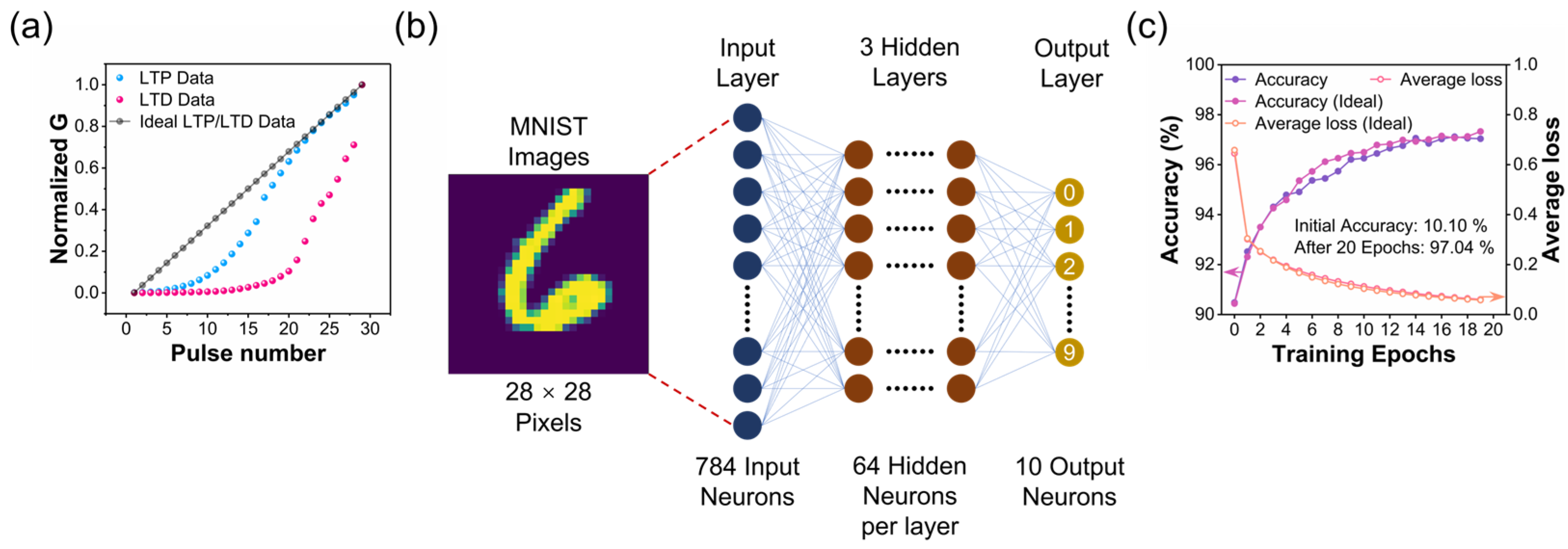
3.2. Long-Term and Short-Term Memory in WO3 ECTs

Figure 5a,b shows the LTP/LTD characteristics of wet-etched WO3 ECTs under varying gate pulse widths and numbers, achieving stable on–off ratios over 103 with an average AR of 0.63 (Table 1).
To emulate synaptic short-term plasticity, paired-pulse facilitation (PPF) was evaluated. A pair of pulses from presynaptic neurons will stimulate postsynaptic neurons to generate two excitatory postsynaptic currents (EPSCs), and the second EPSC is larger than the first one [37,38]. PPF arises from transient H+ adsorption/desorption at the WO3 surface, distinct from the bulk doping responsible for LTP/LTD. Under a positive gate pulse, H+ from Nafion adsorbs onto WO3, forming surface O-H bonds, providing additional carriers in the channel and temporarily increasing channel conductivity IEPSC. Upon pulse removal, internal electric fields drive partial proton desorption, causing IEPSC decay. When a second pulse is applied before complete desorption (∆t < relaxation time), residual adsorbed protons amplify subsequent IEPSC (Figure 5c,d) [16].
The PPF index (I2/I1) increased from 1.01 to 3.38 as ∆t decreased from 800 ms to 50 ms, confirming enhanced short-term memory at shorter intervals [39]. The PPF curve is fitted by a biexponential function [40,41]:
P P F   i n d e x = 1 + A 1   e x p Δ t / τ 1 + A 2   e x p Δ t / τ 2
where τ1 and τ2 correspond to the characteristic relaxation time of H+ after the first and second pulse stimulation [42]. The fitting yielded relaxation times of τ1 = 43.3 ms and τ2 = 218.2 ms. The longer τ2 reflects sustained H+ retention after sequential pulses, enabling short-term cumulative conductance enhancement.
Figure 5e,f demonstrates the stability and endurance of wet-etched ECTs. Twelve distinct conductance states (2 nS–350 μS) were programmed, and all states remained non-overlapping after 103 s of operation in ambient air, confirming robust state retention. Conductance variation within each state was quantified using the coefficient of variation (cv) [43]:
c v = i = 1 m G i G ¯ 2   /   m 1   /   G ¯
where G i is the conductance value sampled at different times, G ¯ is the mean conductance of G i , and m = 201 (5 s sampling interval over 103 s). All states exhibited ultra-low cv < 0.05, indicating minimal conductance drift. Furthermore, the device retained an on–off ratio ~102 after 25 read–write cycles, demonstrating its cycling reliability. The on–off ratio and the number of read–write cycles of ECT are two important parameters in neural morphology calculation. A high on–off ratio can accommodate more storage states, so that there is a larger fault-tolerant interval between the storage states. A sufficient number of cycles can ensure that the conductance drift of the device is negligible when updating conductance, and the conductance can be written accurately.

3.3. Simulated ANN for Image Recognition

To prove the potential of wet-etched ECTs for application in ANNs, a multilayer perceptron (MLP) neural network was constructed by using the Pytorch 1.7.1 platform. The image recognition for the Modified National Institute of Standards and Technology (MNIST) data set was simulated. The normalized LTP/LTD conductance data (Figure 6a, blue and magenta dots) of ECT were used in the weight updating process of the ANN, as shown in Figure 6a. As a comparison, an ideal datapoint (Figure 6a, gray dots) is generated from the computer as the case with best linearity.
Figure 6b represents the MLP neural network model consisting of 784 input neurons, 64 × 3 hidden neurons, and 10 output neurons, respectively. The training and recognition process of the ANN was carried out in a training data set containing 60,000 images and a separate test data set containing 10,000 images, respectively. As for the weight updating method, based on Adam optimizer, we rewrite a gradient optimizer of discrete pulse coding, which realizes the pulse quantization of weight updating through a bio-inspired LTP and LTD look-up table (LUT). On the basis of retaining the adaptive learning rate characteristics of Adam optimizer, this optimizer replaces the continuous gradient update value with discrete pulse amplitude. Specifically, consistent with the traditional Adam optimizer, it first calculates the first moment (momentum) m and the second moment (variance) v of the gradient, and then calculates the original weight update amount Δw; on this basis, the continuous update amount Δw is realized by double look-up table (LTP/LTD-LUT). Then, we multiply it by the learning rate to obtain the final weight update.
As seen in Figure 6c, wet-etched ECT displayed ~97.04% image recognition accuracy after 20 epochs, while the accuracy of the ideal device was ~97.33%. The corresponding average loss decreased from 0.650 to 0.061 after 20 epochs for the experimental device and decreased from 0.659 to 0.058 for the ideal device. The accuracy for the experimental data is close to that for the ideal case. The reason is likely the training gradient in the early stages of the MLP. Consequently, the weights trained in the original code primarily utilize the first half of the LTP/LTD data. This subset is highly linear and sufficiently dense to cover the normalized conductance range of 0–0.4, thereby improving convergence speed and accuracy. These results demonstrate that wet-etched ECTs can realize high-accuracy image recognition of handwritten numerals, as well as perform multilevel data storage and neuromorphic computing [44,45].
The above algorithm and simulation can be extended in platforms, such as MATLAB R2022b and SPICE (PySpice1.5), that can be combined with the Python 3.8 interface. For hardware implementation, this algorithm can be conducted by a hybrid computing architecture with a field programmable gate array (FPGA) and ECT array. The FPGA, as a digital controller, executes the gradient calculation, LUT query, and other logical operations. As an analog computing unit, the ECT array encodes input pulse, stores the weight values, and realizes multiplication and addition operations [46,47,48].
As a comparison, we summarized the performance of the existing advanced ECTs and the results of this work in Table 2. The ECT in this work shows balance performance on the on–off ratio, retention time, and recognition accuracy in the simulated neural network.

4. Conclusions

We developed a novel wet etching process for WO3 patterning, enabling the fabrication of Nafion–WO3 ECTs with sol–gel-derived WO3 channels. The wet-etched ECTs achieved an on–off ratio of ~105, outperforming unetched and dry-etched devices by orders of magnitude. These devices also exhibited excellent paired-pulse facilitation (PPF) and long-term stability, maintaining 12 distinct conductance states for 103 s and retaining an on–off ratio of ~102 over 25 read–write cycles. XPS analysis confirmed that wet etching enhanced H+ injection efficiency, with higher W5⁺ and M-O-H content compared to dry etching, leading to more thorough electrochemical reactions and superior device performance. The ANN simulation using this wet-etched ECT showed ~97% image recognition accuracy for handwritten numerals. The average loss of wet-etched ECT decreased from 0.65 to 0.06 after 20 epochs. This work demonstrates that wet etching is a promising approach for scalable, high-performance neuromorphic devices.

Author Contributions

Device design, L.Z. (Liwei Zhang); fabrication, L.Z. (Liwei Zhang); characterization, L.Z. (Liwei Zhang); image recognition, S.C., L.Z. (Liwei Zhang); writing—original draft preparation, L.Z. (Liwei Zhang), S.C., S.F., S.H., L.Z. (Li Zhang), Y.Z., M.W., X.L. and C.L. All authors have read and agreed to the published version of the manuscript.

Funding

This research was funded by the National Natural Science Foundation of China (62404255).

Data Availability Statement

The data presented in this study are available from the corresponding author upon reasonable request.

Acknowledgments

The authors gratefully acknowledge the technical support from the Laboratory Teaching Center of Electronics and Information Technology in Sun Yat-sen University.

Conflicts of Interest

The authors declare no conflicts of interest.

References

  1. Ielmini, D.; Ambrogio, S. Emerging neuromorphic devices. Nanotechnology 2020, 31, 092001. [Google Scholar] [CrossRef] [PubMed]
  2. Zhu, J.; Zhang, T.; Yang, Y.; Huang, R. A comprehensive review on emerging artificial neuromorphic devices. Appl. Phys. Rev. 2020, 7, 011312. [Google Scholar] [CrossRef]
  3. Boahen, K. A neuromorph’s prospectus. Comput. Sci. Eng. 2017, 19, 14–28. [Google Scholar] [CrossRef]
  4. Wang, T.; Meng, J.; Zhou, X.; Liu, Y.; He, Z.; Han, Q.; Li, Q.; Yu, J.; Li, Z.; Liu, Y.; et al. Reconfigurable neuromorphic memristor network for ultralow-power smart textile electronics. Nat. Commun. 2022, 13, 7432. [Google Scholar] [CrossRef]
  5. Wang, L.; Zhang, P.; Gao, Z.; Wen, D. Artificial Tactile Sensing Neuron with Tactile Sensing Ability Based on a Chitosan Memristor. Adv. Sci. 2024, 11, 2308610. [Google Scholar] [CrossRef] [PubMed]
  6. Park, S.-O.; Hong, S.; Sung, S.-J.; Kim, D.; Seo, S.; Jeong, H.; Park, T.; Cho, W.J.; Kim, J.; Choi, S. Phase-change memory via a phase-changeable self-confined nano-filament. Nature 2024, 628, 293–298. [Google Scholar] [CrossRef] [PubMed]
  7. Burr, G.W.; Breitwisch, M.J.; Franceschini, M.; Garetto, D.; Gopalakrishnan, K.; Jackson, B.; Kurdi, B.; Lam, C.; Lastras, L.A.; Padilla, A.; et al. Phase change memory technology. J. Vac. Sci. Technol. B 2010, 28, 223–262. [Google Scholar] [CrossRef]
  8. Si, M.; Su, C.-J.; Jiang, C.; Conrad, N.J.; Zhou, H.; Maize, K.D.; Qiu, G.; Wu, C.-T.; Shakouri, A.; Alam, M.A.; et al. Steep-slope hysteresis-free negative capacitance MoS2 transistors. Nat. Nanotechnol. 2018, 13, 24–28. [Google Scholar] [CrossRef]
  9. Gao, L.; Hu, B.-L.; Wang, L.; Cao, J.; He, R.; Zhang, F.; Wang, Z.; Xue, W.; Yang, H.; Li, R.-W. Intrinsically elastic polymer ferroelectric by precise slight cross-linking. Science 2023, 381, 540–544. [Google Scholar] [CrossRef]
  10. van de Burgt, Y.; Lubberman, E.; Fuller, E.J.; Keene, S.T.; Faria, G.C.; Agarwal, S.; Marinella, M.J.; Alec Talin, A.; Salleo, A. A non-volatile organic electrochemical device as a low-voltage artificial synapse for neuromorphic computing. Nat. Mater. 2017, 16, 414–418. [Google Scholar] [CrossRef]
  11. Tang, J.; Bishop, D.; Kim, S.; Copel, M.; Gokmen, T.; Todorov, T.; Shin, S.; Lee, K.T.; Solomon, P.; Chan, K.; et al. ECRAM as Scalable Synaptic Cell for High-Speed, Low-Power Neuromorphic Computing. In Proceedings of the 2018 IEEE International Electron Devices Meeting (IEDM), San Francisco, CA, USA, 1–5 December 2018. [Google Scholar] [CrossRef]
  12. Yang, C.-S.; Shang, D.-S.; Liu, N.; Fuller, E.J.; Agrawal, S.; Talin, A.A.; Li, Y.-Q.; Shen, B.-G.; Sun, Y. All-Solid-State Synaptic Transistor with Ultralow Conductance for Neuromorphic Computing. Adv. Funct. Mater. 2018, 28, 1804170. [Google Scholar] [CrossRef]
  13. Milewska, A.; Świerczek, K.; Tobola, J.; Boudoire, F.; Hu, Y.; Bora, D.K.; Mun, B.S.; Braun, A.; Molenda, J. The nature of the nonmetal–metal transition in LixCoO2 oxide. Solid State Ion. 2014, 263, 110–118. [Google Scholar] [CrossRef]
  14. Speulmanns, J.; Kia, A.M.; Kühnel, K.; Bönhardt, S.; Weinreich, W. Surface-Dependent Performance of Ultrathin TiN Films as an Electrically Conducting Li Diffusion Barrier for Li-Ion-Based Devices. ACS Appl. Mater. Interfaces 2020, 12, 39252–39260. [Google Scholar] [CrossRef]
  15. Huang, J.; Wu, K.; Xu, G.; Wu, M.; Dou, S.; Wu, C. Recent progress and strategic perspectives of inorganic solid electrolytes: Fundamentals, modifications, and applications in sodium metal batteries. Chem. Soc. Rev. 2023, 52, 4933–4995. [Google Scholar] [CrossRef]
  16. Yang, C.S.; Shang, D.S.; Liu, N.; Shi, G.; Shen, X.; Yu, R.C.; Li, Y.Q.; Sun, Y. A Synaptic Transistor based on Quasi-2D Molybdenum Oxide. Adv. Mater. 2017, 29, 1700906. [Google Scholar] [CrossRef]
  17. Zhang, F.; Zhang, Y.; Li, L.; Mou, X.; Peng, H.; Shen, S.; Wang, M.; Xiao, K.; Ji, S.-H.; Yi, D.; et al. Nanoscale multistate resistive switching in WO3 through scanning probe induced proton evolution. Nat. Commun. 2023, 14, 3950. [Google Scholar] [CrossRef]
  18. Yao, X.; Klyukin, K.; Lu, W.; Onen, M.; Ryu, S.; Kim, D.; Emond, N.; Waluyo, I.; Hunt, A.; del Alamo, J.A.; et al. Protonic solid-state electrochemical synapse for physical neural networks. Nat. Commun. 2020, 11, 3134. [Google Scholar] [CrossRef]
  19. Tran, D.M.; Son, J.W.; Ju, T.-S.; Hwang, C.; Park, B.H. Dopamine-Regulated Plasticity in MoO3 Synaptic Transistors. ACS Appl. Mater. Interfaces 2023, 15, 49329–49337. [Google Scholar] [CrossRef]
  20. Li, Y.; Lu, J.; Shang, D.; Liu, Q.; Wu, S.; Wu, Z.; Zhang, X.; Yang, J.; Wang, Z.; Lv, H.; et al. Oxide-Based Electrolyte-Gated Transistors for Spatiotemporal Information Processing. Adv. Mater. 2020, 32, 2003018. [Google Scholar] [CrossRef]
  21. Sahu, M.C.; Jena, A.K.; Mallik, S.K.; Roy, S.; Sahoo, S.; Ajimsha, R.S.; Misra, P.; Sahoo, S. Reconfigurable Low-Power TiO2 Memristor for Integration of Artificial Synapse and Nociceptor. ACS Appl. Mater. Interfaces 2023, 15, 25713–25725. [Google Scholar] [CrossRef]
  22. Xu, H.; Shang, D.; Luo, Q.; An, J.; Li, Y.; Wu, S.; Yao, Z.; Zhang, W.; Xu, X.; Dou, C.; et al. A low-power vertical dual-gate neurotransistor with short-term memory for high energy-efficient neuromorphic computing. Nat. Commun. 2023, 14, 6385. [Google Scholar] [CrossRef] [PubMed]
  23. Vemuri, R.S.; Engelhard, M.H.; Ramana, C.V. Correlation between Surface Chemistry, Density, and Band Gap in Nanocrystalline WO3 Thin Films. ACS Appl. Mater. Interfaces 2012, 4, 1371–1377. [Google Scholar] [CrossRef]
  24. Xie, D.; Liang, X.; Geng, D.; Wu, Q.; Liu, C. An Enhanced Synaptic Plasticity of Electrolyte-Gated Transistors through the Tungsten Doping of an Oxide Semiconductor. Electronics 2024, 13, 1485. [Google Scholar] [CrossRef]
  25. Hjelm, A.; Granqvist, C.G.; Wills, J.M. Electronic structure and optical properties of WO3, LiWO3, NaWO3, and HWO3. Phys. Rev. B 1996, 54, 2436–2445. [Google Scholar] [CrossRef]
  26. Talin, A.A.; Li, Y.; Robinson, D.A.; Fuller, E.J.; Kumar, S. ECRAM Materials, Devices, Circuits and Architectures: A Perspective. Adv. Mater. 2023, 35, 2204771. [Google Scholar] [CrossRef] [PubMed]
  27. Cui, J.; An, F.; Qian, J.; Wu, Y.; Sloan, L.L.; Pidaparthy, S.; Zuo, J.-M.; Cao, Q. CMOS-compatible electrochemical synaptic transistor arrays for deep learning accelerators. Nat. Electron. 2023, 6, 292–300. [Google Scholar] [CrossRef]
  28. Johnson, N.R.; George, S.M. WO3 and W Thermal Atomic Layer Etching Using “Conversion-Fluorination” and “Oxidation-Conversion-Fluorination” Mechanisms. ACS Appl. Mater. Interfaces 2017, 9, 34435–34447. [Google Scholar] [CrossRef]
  29. Su, X.; Li, Y.; Jian, J.; Wang, J. In situ etching WO3 nanoplates: Hydrothermal synthesis, photoluminescence and gas sensor properties. Mater. Res. Bull. 2010, 45, 1960–1963. [Google Scholar] [CrossRef]
  30. Shi, P.; Wang, D.; Yu, T.; Xing, R.; Wu, Z.; Yan, S.; Wei, L.; Chen, Y.; Ren, H.; Yu, C.; et al. Solid-state electrolyte gated synaptic transistor based on SrFeO2.5 film channel. Mater. Des. 2021, 210, 110022. [Google Scholar] [CrossRef]
  31. Jang, J.W.; Park, S.; Burr, G.W.; Hwang, H.; Jeong, Y.H. Optimization of Conductance Change in Pr1–xCaxMnO3-Based Synaptic Devices for Neuromorphic Systems. IEEE Electron Device Lett. 2015, 36, 457–459. [Google Scholar] [CrossRef]
  32. Wang, I.T.; Chang, C.-C.; Chiu, L.-W.; Chou, T.; Hou, T.-H. 3D Ta/TaOx/TiO2/Ti synaptic array and linearity tuning of weight update for hardware neural network applications. Nanotechnology 2016, 27, 365204. [Google Scholar] [CrossRef] [PubMed]
  33. Wu, Z.; Shi, P.; Xing, R.; Xing, Y.; Ge, Y.; Wei, L.; Wang, D.; Zhao, L.; Yan, S.; Chen, Y. Quasi-two-dimensional α-molybdenum oxide thin film prepared by magnetron sputtering for neuromorphic computing. RSC Adv. 2022, 12, 17706–17714. [Google Scholar] [CrossRef] [PubMed]
  34. Zhang, G.; Guo, K.; Shen, X.; Ning, H.; Liang, H.; Zhong, J.; Xu, W.; Tang, B.; Yao, R.; Peng, J. Physical Simulation Model of WO3 Electrochromic Films Based on Continuous Electron-Transfer Kinetics and Experimental Verification. ACS Appl. Mater. Interfaces 2021, 13, 4768–4776. [Google Scholar] [CrossRef]
  35. Bathe, S.R.; Patil, P.S. Titanium doping effects in electrochromic pulsed spray pyrolysed WO3 thin films. Solid State Ion. 2008, 179, 314–323. [Google Scholar] [CrossRef]
  36. Karbalaei Akbari, M.; Ramachandran, R.K.; Detavernier, C.; Hu, J.; Kim, J.; Verpoort, F.; Zhuiykov, S. Heterostructured plasmonic memristors with tunable opto-synaptic functionalities. J. Mater. Chem. C 2021, 9, 2539–2549. [Google Scholar] [CrossRef]
  37. He, Y.; Nie, S.; Liu, R.; Shi, Y.; Wan, Q. Indium–Gallium–Zinc–Oxide Schottky Synaptic Transistors for Silent Synapse Conversion Emulation. IEEE Electron Device Lett. 2019, 40, 139–142. [Google Scholar] [CrossRef]
  38. Zhou, J.; Wan, C.; Zhu, L.; Shi, Y.; Wan, Q. Synaptic Behaviors Mimicked in Flexible Oxide-Based Transistors on Plastic Substrates. IEEE Electron Device Lett. 2013, 34, 1433–1435. [Google Scholar] [CrossRef]
  39. Han, C.; Han, X.; Han, J.; He, M.; Peng, S.; Zhang, C.; Liu, X.; Gou, J.; Wang, J. Light-Stimulated Synaptic Transistor with High PPF Feature for Artificial Visual Perception System Application. Adv. Funct. Mater. 2022, 32, 2113053. [Google Scholar] [CrossRef]
  40. Gong, Y.; Wang, Y.; Li, R.; Yang, J.-Q.; Lv, Z.; Xing, X.; Liao, Q.; Wang, J.; Chen, J.; Zhou, Y.; et al. Tailoring synaptic plasticity in a perovskite QD-based asymmetric memristor. J. Mater. Chem. C 2020, 8, 2985–2992. [Google Scholar] [CrossRef]
  41. Zucker, R.S.; Regehr, W.G. Short-Term Synaptic Plasticity. Annu. Rev. Physiol. 2002, 64, 355–405. [Google Scholar] [CrossRef]
  42. Zinebi, F.; Russell, R.T.; McKernan, M.; Shinnick-Gallagher, P. Comparison of paired-pulse facilitation of AMPA and NMDA synaptic currents in the lateral amygdala. Synapse 2001, 42, 115–127. [Google Scholar] [CrossRef] [PubMed]
  43. Brenes, A.J. Calculating and Reporting Coefficients of Variation for DIA-Based Proteomics. J. Proteome Res. 2024, 23, 5274–5278. [Google Scholar] [CrossRef] [PubMed]
  44. Chen, P.Y.; Peng, X.; Yu, S. NeuroSim+: An integrated device-to-algorithm framework for benchmarking synaptic devices and array architectures. In Proceedings of the 2017 IEEE International Electron Devices Meeting (IEDM), San Francisco, CA, USA, 2–6 December 2017. [Google Scholar] [CrossRef]
  45. Mohanty, H.N.; Tsuruoka, T.; Mohanty, J.R.; Terabe, K. Proton-Gated Synaptic Transistors, Based on an Electron-Beam Patterned Nafion Electrolyte. ACS Appl. Mater. Interfaces 2023, 15, 19279–19289. [Google Scholar] [CrossRef] [PubMed]
  46. Nowshin, F.; Yi, Y. Memristor-based Deep Spiking Neural Network with a Computing-In-Memory Architecture. In Proceedings of the 2022 23rd International Symposium on Quality Electronic Design (ISQED), Santa Clara, CA, USA, 6–7 April 2022. [Google Scholar] [CrossRef]
  47. Yao, P.; Wu, H.; Gao, B.; Tang, J.; Zhang, Q.; Zhang, W.; Yang, J.J.; Qian, H. Fully hardware-implemented memristor convolutional neural network. Nature 2020, 577, 641–646. [Google Scholar] [CrossRef] [PubMed]
  48. Burr, G.W.; Shelby, R.M.; Sebastian, A.; Kim, S.; Kim, S.; Sidler, S.; Virwani, K.; Ishii, M.; Narayanan, P.; Fumarola, A.; et al. Neuromorphic computing using non-volatile memory. Adv. Phys. X 2017, 2, 89–124. [Google Scholar] [CrossRef]
  49. Wu, Z.; Shi, P.; Xing, R.; Yu, T.; Zhao, L.; Wei, L.; Wang, D.; Yan, S.; Tian, Y.; Bai, L.; et al. Flexible Mott Synaptic Transistor on Polyimide Substrate for Physical Neural Networks. Adv. Electron. Mater. 2022, 8, 2200078. [Google Scholar] [CrossRef]
  50. Su, D.; Liang, X.; Geng, D.; Wu, Q.; Liu, B.; Liu, C. An Artificial Neural Network Based on Oxide Synaptic Transistor for Accurate and Robust Image Recognition. Micromachines 2024, 15, 433. [Google Scholar] [CrossRef]
Figure 1. (a) Schematic diagram of the fabrication process of Nafion–WO3 ECT. The optical microscope image of the patterned WO3 (left) and the high magnification optical microscope image of the edge of patterned WO3 (right) treated by (b) dry etching with RIE, (c) wet etching with TMAH. (d) The atomic force microscope (AFM) images of the above three devices.
Electronics 14 01183 g001
Figure 2. The transfer and output characteristics of WO3-based ECTs: (a) no etching, (b) dry etching, (c) wet etching.
Electronics 14 01183 g002
Figure 3. The LTP/LTD characteristics for the WO3-based ECT (a) without etching, with (b) dry etching and (c) wet etching under different gate pulse amplitudes. The corresponding (d) on–off conductance ratio and (e) asymmetric ratio (AR).
Electronics 14 01183 g003
Figure 4. The X-ray photoelectron spectroscopy of W4f and O1s for the WO3 (ad) without etching, with (eh) dry etching, and with (il) wet etching, where WO3 and HxWO3 are the channel before and after protons injection. The percentage changes of (m) W content at different valence states and (n) O content at different binding states.
Electronics 14 01183 g004
Figure 5. The performance of ECT processed by TMAH wet etching. The LTP/LTD characteristics measured (a) at different gate pulse widths (50 ms, 100 ms, 200 ms), and constant amplitude (500 nA) (b) at different numbers of positive and negative pulses (15p + 15d, 30p + 30d, 50p + 50d) and constant amplitude (500 nA) and width (50 ms). (c) Excitatory post synaptic currents I1 and I2 at VDS = 1 V triggered by a pair of gate voltage pulses. The amplitude, width, and duty cycle of the gate voltage pulse are 1.5 V, 200 ms, and 50%, respectively. (d) The PPF index is a function of the pulse interval time ∆t, and it is fitted by a double-phase exponential function. (e) The retention time of ECT in multiple conductance states (VDS = 1 V), and (f) the endurance of the read–write cycle (VDS = 1 V, the gate pulse amplitude, width, and number are 500 nA, 50 ms, and 10p + 10d, respectively).
Electronics 14 01183 g005
Figure 6. (a) The LTP/LTD data of the wet-etched ECT and ideal ECT are, respectively, used in the weight updating process of the neural network. (b) The structure diagram of the neural network model used to simulate the image recognition of 28 × 28-pixel handwritten numerals from the MNIST data set. (c) The diagram of image recognition accuracy and average loss with training epochs using the wet-etched and ideal ECT, respectively.
Electronics 14 01183 g006
Table 1. The on–off ratio and asymmetry ratio of ECT with wet etching under different gate pulse widths or numbers.
Pulse Width/NumberGmax/GminAR A R ¯
50 ms259.00.67
100 ms1731.10.68
200 ms3192.40.89
0.63
15p + 15d259.00.67
30p + 30d859.20.58
50p + 50d3652.00.31
Table 2. The comparison between the existing advanced ECTs and the results of this work.
ChannelElectrolyteIon TypeOn-Off RatioConductance
Retention Time
Recognition
Accuracy
Ref.
MoO3H2SO4H+~250 s-[16]
Nb2O5LixSiO2Li+~20103 s-[20]
VO2CsClO4H+~24 × 103 s98%[49]
In2O3Al2O3H+~3120 s85%[50]
WO3ZrO2H+~20103 s93%[27]
IZONafionH+~2.5103 s84%[45]
WO3NafionH+~107--[18]
WO3NafionH+~105103 s97%Our work
Disclaimer/Publisher’s Note: The statements, opinions and data contained in all publications are solely those of the individual author(s) and contributor(s) and not of MDPI and/or the editor(s). MDPI and/or the editor(s) disclaim responsibility for any injury to people or property resulting from any ideas, methods, instructions or products referred to in the content.

