
Radiation-Hardened Design and Experimental Validation Using a Mixed-Stage Model for Reliability Assessment of Integrated Circuits in Radiation Environments

Abstract
1. Introduction
2. Optimization of Radiation-Hardened Layouts for CMOS Devices
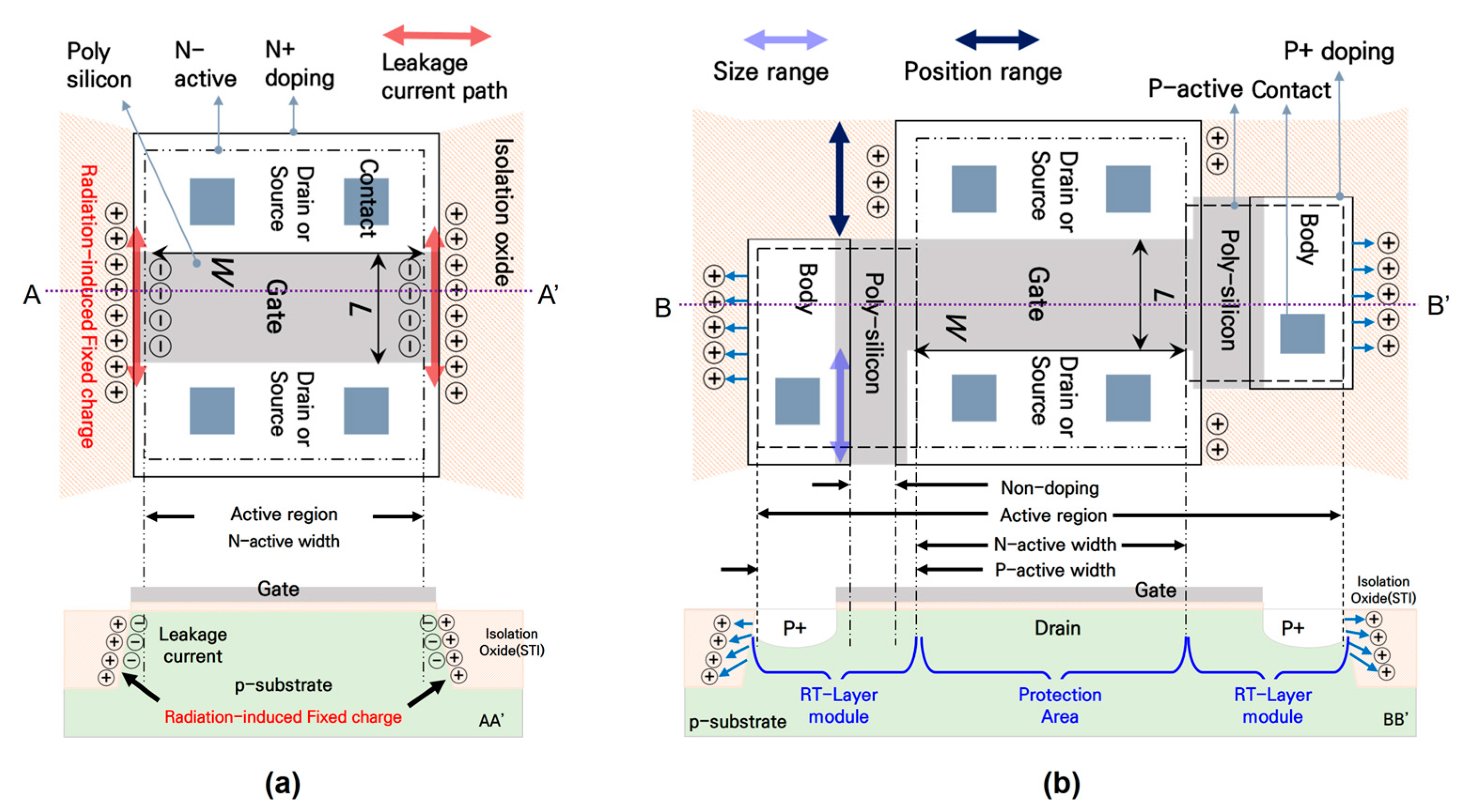
2.1. Total Ionizing Dose Effects in CMOS Devices
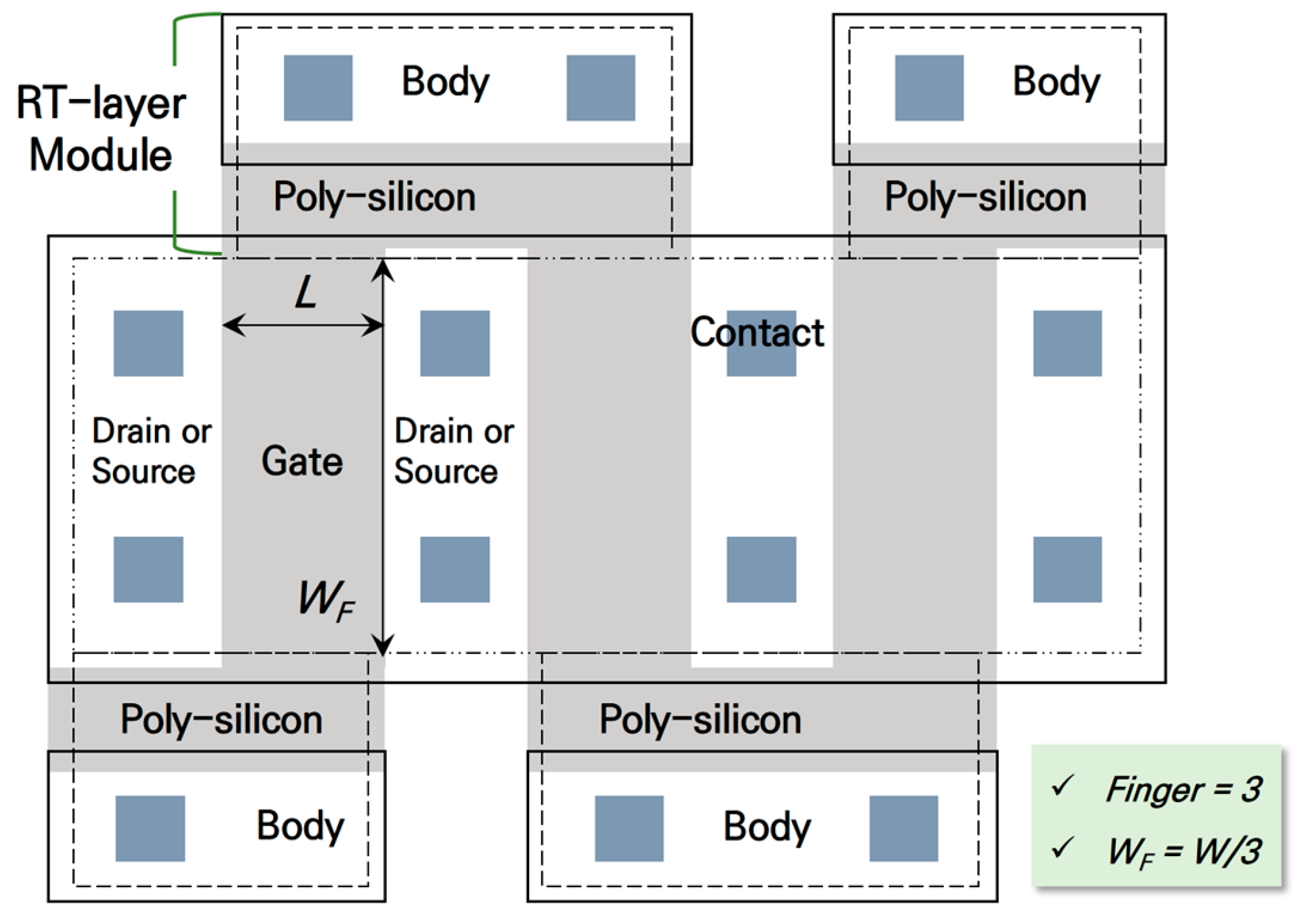
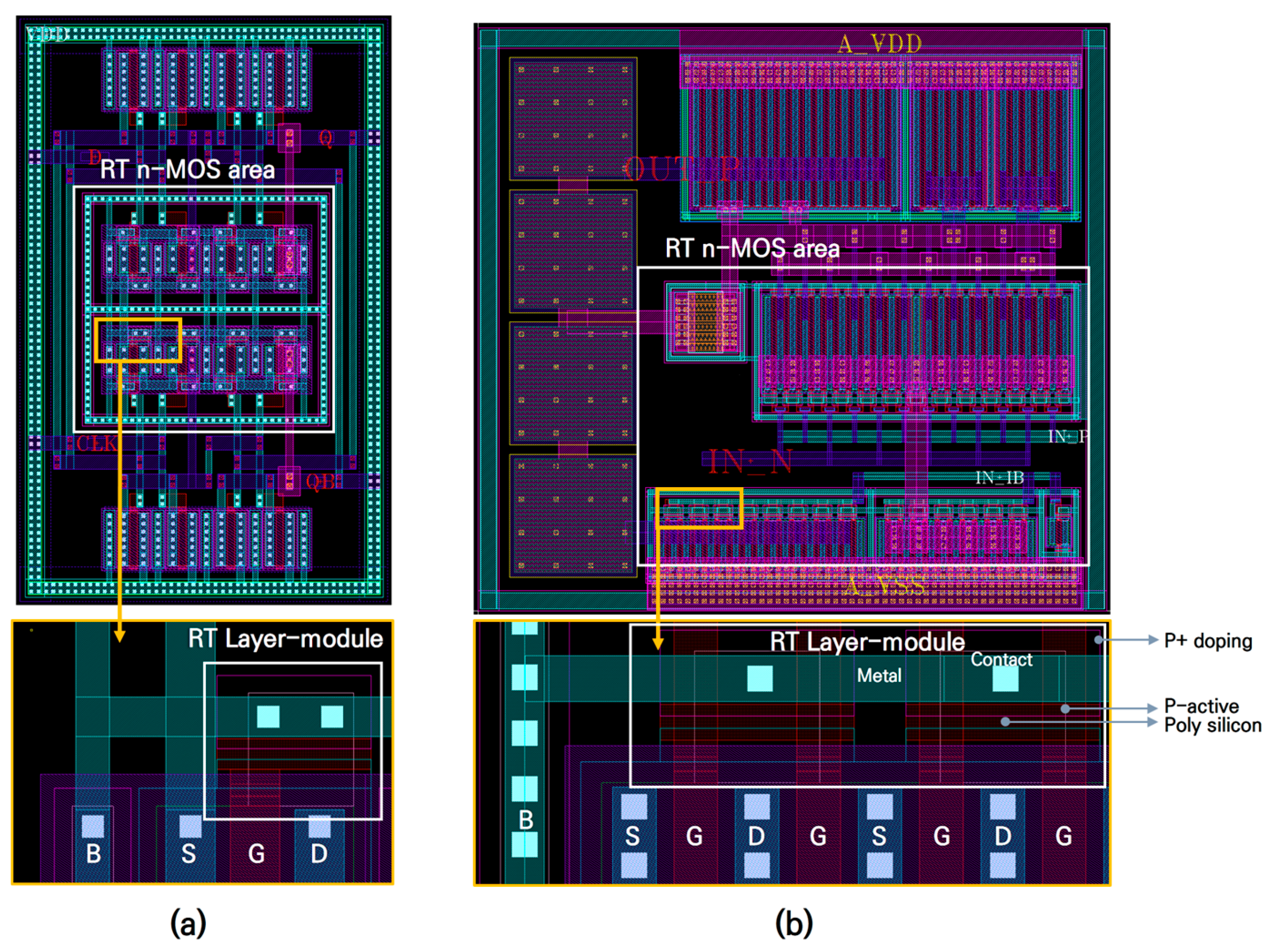
2.2. Radiation-Hardened Structure Design for CMOS Devices
3. Radiation-Tolerant IC M&S and Implementation
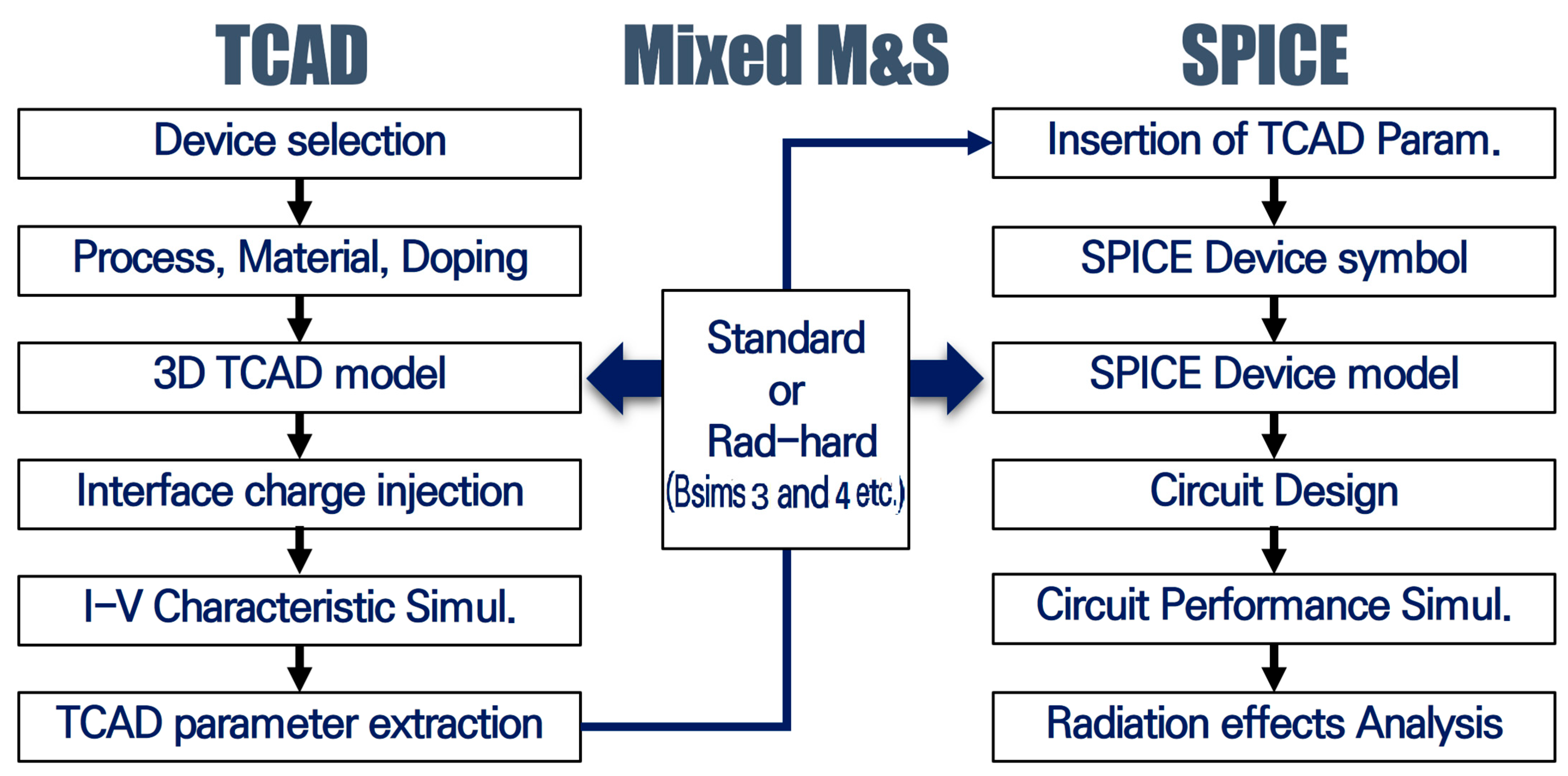
3.1. Mixed-Stage M&S for ASIC Radiation Effects
3.2. Radiation-Tolerant CMOS ASIC Design and Fabrication
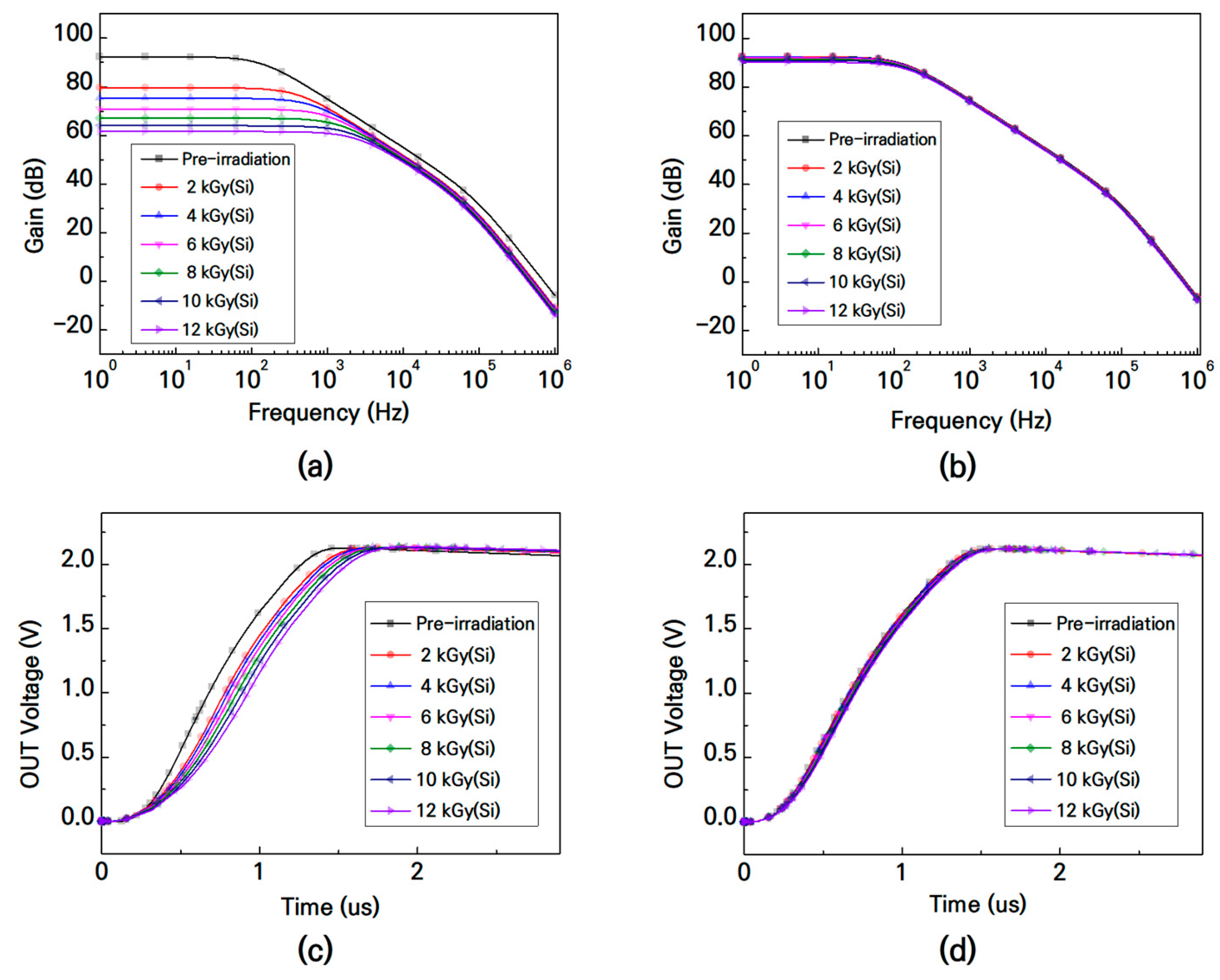
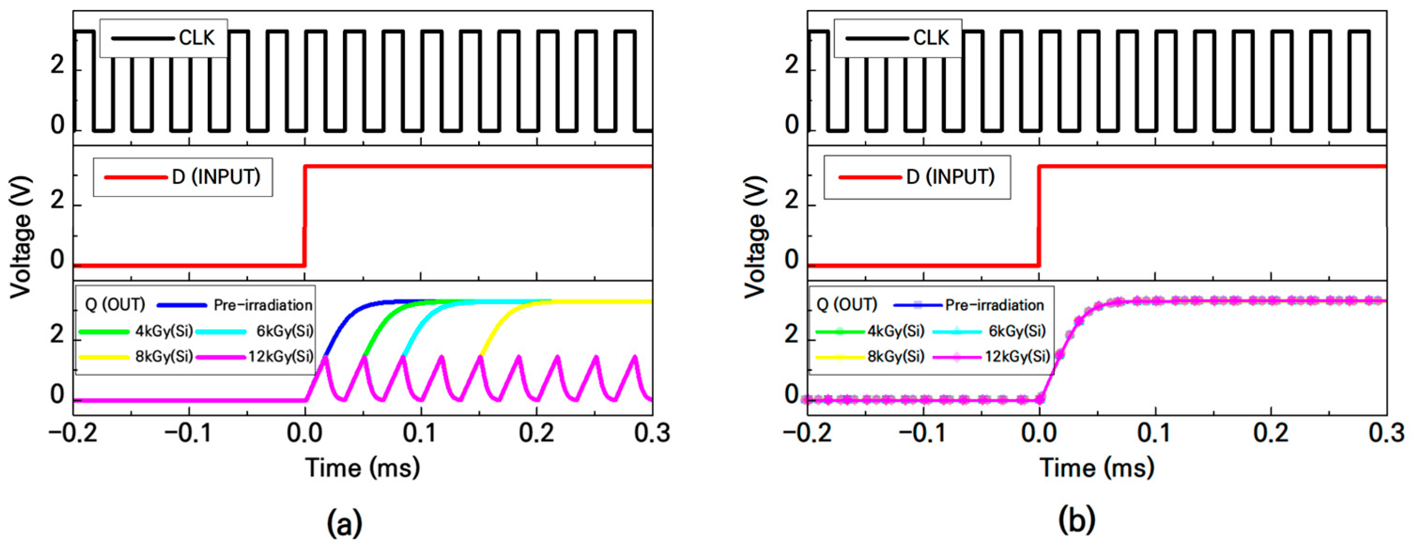
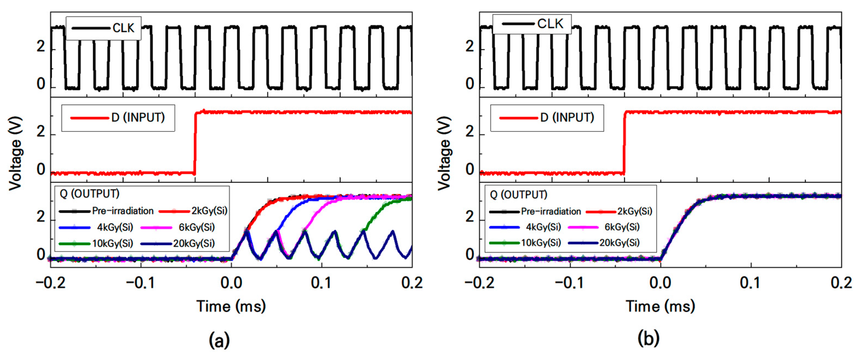
4. Experimental Validation of Radiation-Tolerant ICs
4.1. TID Testing of Proposed Radiation-Tolerant ASIC Chips
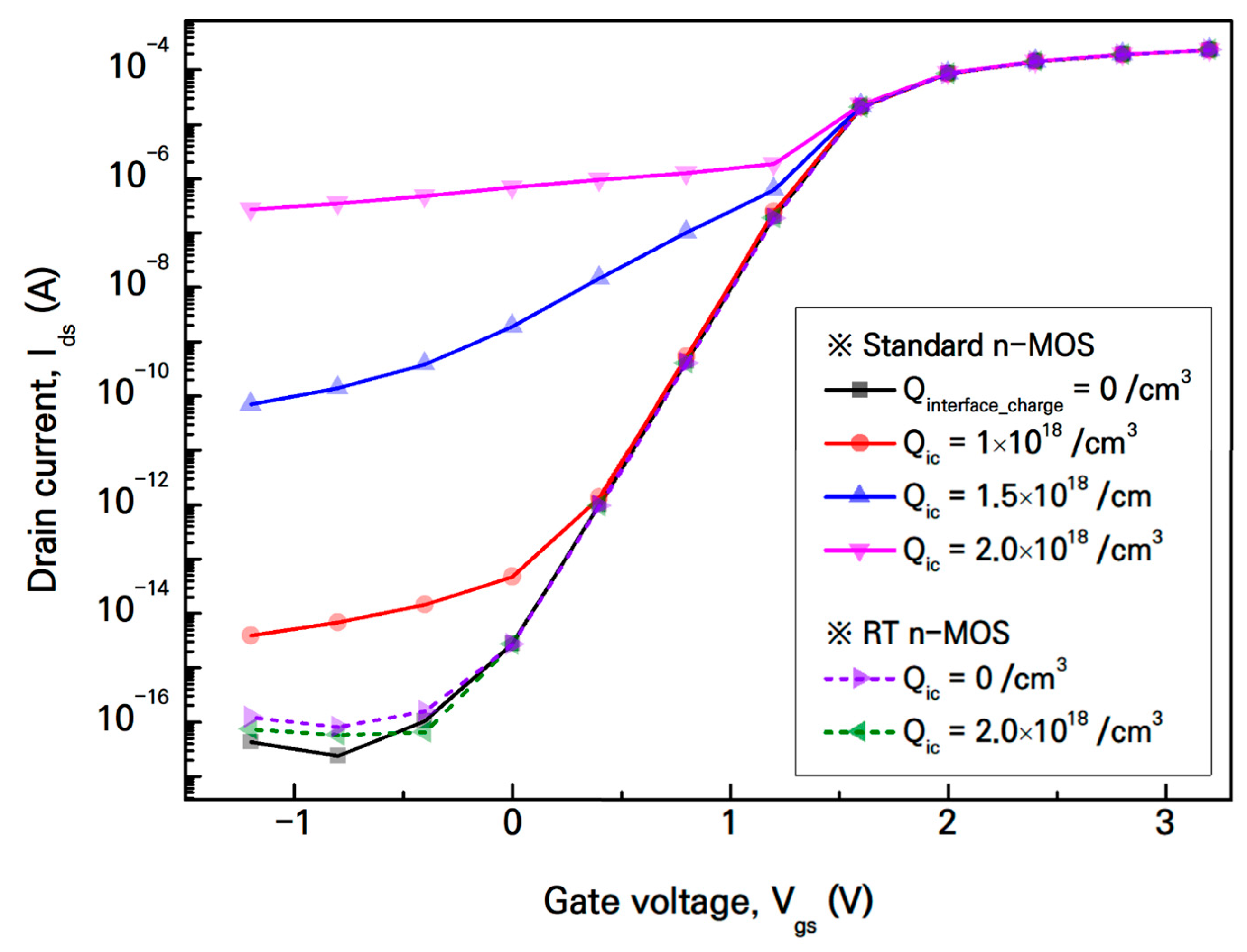
4.2. Radiation Test Results and Analysis
5. Conclusions
Author Contributions
Funding
Data Availability Statement
Acknowledgments
Conflicts of Interest
References
- Conrad, E.E. Radiation effects research in the 60’s. IEEE Trans. Nucl. Sci. 1994, 41, 2648–2659. [Google Scholar] [CrossRef]
- Holmes-Siedle, A.; Adams, L. Handbook of Radiation Effects, 2nd ed.; Oxford University Press: Oxford, UK, 2002. [Google Scholar]
- Cohn, L.; Espig, M.; Wolicki, A.; Simons, M.; Rogers, C. Transient Radiation Effects on Electronics (TREE) Handbook; Defense Nuclear Agency: Fort Belvoir, VA, USA, 1996. [Google Scholar]
- Messenger, G.C.; Ash, M.S. The Effects of Radiation on Electronic Systems; Springer Press: New York, NY, USA; Van Nostrand Reihnold: New York, NY, USA, 1992. [Google Scholar]
- Joop, M.K.Q.; Moaiyeri, M.H.; Shidaifat, A.A.; Song, H. Ultra-Efficient and Robust Auto-Nonvolatile Schmitt Trigger-Based Latch Design Using Ferroelectric CNTFET Technology. IEEE Trans. Ultrason. Ferroelectr. Freq. Control 2022, 69, 1829–1840. [Google Scholar] [CrossRef]
- Schwank, J.R.; Sexton, F.W.; Shaneyfelt, M.R.; Fleetwood, D.M. Total ionizing dose hardness assurance issues for high dose rate environments. IEEE Trans. Nucl. Sci. 2007, 54, 1042–1048. [Google Scholar] [CrossRef]
- Snoeys, W.J.; Gutierrez, T.A.P.; Anelli, G. A New NMOS Layout Structure for Radiation Tolerance. IEEE Trans. Nul. Sci. 2002, 49, 1829–1833. [Google Scholar] [CrossRef]
- Giraldo, A.; Paccagnella, A.; Minzoni, A. Aspect ratio calculation in n-channel MOSFET’s with a gate-enclosed layout. Solid State Electron. 2000, 44, 981–989. [Google Scholar] [CrossRef]
- Lee, M.S.; Lee, H.C. Dummy gate- assisted n-MOSFET layout for a radiation-tolerant integrated circuit. IEEE Trans. Nucl. Sci. 2013, 60, 3084–3091. [Google Scholar] [CrossRef]
- Liu, Z.; Yu, H.; Liu, Y.; Ning, H. Design of a Radiation Hardened DC-DC Boost Converter. In Proceedings of the Information Engineering and Computer Science (ICIECS), 2010 2nd International Conference, Wuhan, China, 25–26 December 2010. [Google Scholar] [CrossRef]
- Saks, N.S.; Ancona, M.G.; Modolo, J.A. Generation of interface states by ionizing radiation in very thin MOS oxides. IEEE Trans. Nucl. Sci. 1986, 33, 1185–1190. [Google Scholar] [CrossRef]
- Barnaby, H.J. Total-ionizing-dose effects in modern CMOS technologies. IEEE Trans. Nucl. Sci. 2006, 53, 3103–3121. [Google Scholar] [CrossRef]
- Kumar, M.; Ubhi, J.S.; Basra, S.; Chawla, A.; Jatana, H.S. Total ionizing dose hardness analysis of transistors in commercial 180 nm CMOS technology. Microelectron. J. 2021, 115, 105182. [Google Scholar] [CrossRef]
- Oldham, T.R.; Mclean, F.B. Total ionizing dose effects in MOS oxides and devices. IEEE Trans. Nucl. Sci. 2003, 50, 483–499. [Google Scholar] [CrossRef]
- Baker, R.J. CMOS: Circuit Design, Layout, and Simulation, 3rd ed.; John Wiley & Sons Ltd.: Hoboken, NJ, USA, 2010. [Google Scholar]
- Hastings, A. The Art of Analog Layout, 2nd ed.; Prentice Hall: Hoboken, NJ, USA, 2005. [Google Scholar]
- Korea Atomic Energy Institute. Jeongeup-si, South Korea. Advanced Radiation Technology Institute. Available online: https://www.kaeri.re.kr/arti/ (accessed on 17 October 2024).
- Ionizing Radiation (Total Dose) Test Procedure; MIL-STD-883H 1019.8; United States Department of Defense: Arlington County, VA, USA, 2010.
- Total Dose Steady-State Irradiation Test Method; ESA/SCC Basic Specification; European Space Agency: Paris, France, 2010; Volume 22900.


| Comparison Criteria | M&S Methods for Radiation Effects on ICs | ||
|---|---|---|---|
| Full-TCAD | Full-SPICE | Mixed-Stage (This Work) | |
| Computation Time | Very Long | Short | Moderate |
| Accuracy | Very High | Low | Medium to High |
| Modeling Precision | Device-Level | Circuit-Level | Device + Circuit-Level |
| Scalability with Complexity Increase | Low | High | Moderate |
| Applicability to Large Circuits | Small-Scale Transistor | Large-Scale System Analysis | Mid-Scale IC Analysis |
| SPICE Model Extracted from TCAD | ||
|---|---|---|
| Parameter | Description | TID Effects |
| VTH0 | Initial threshold voltage | Increases |
| U0 | Low-field mobility | Decreases |
| ETA0 | Drain-Induced Barrier Lowering (DIBL) coefficient | Increases |
| NFS | Fixed oxide charge density | Increases |
| XJ | Junction depth | Increases |
| WD | Depletion width | Increases |
| IS | Saturation current | Increases |
| Measurement Conditions | ||
|---|---|---|
| Irradiation conditions | Total dose [kGy(Si)] | 20 |
| Dose rate [kGy/h] | 5 | |
| RT-IC type (1) | Driver buffer with RT Op-Amp | |
| Bias conditions | Supply voltage [V] | 3.3 |
| Input | Unit step function/0~2 V | |
| Term of elec. parameter | Slew rate [V/us] | |
| RT-IC type (2) | RT D-latch | |
| Bias conditions | Supply voltage [V] | 3.3 |
| Input (D) | pulse/100 Hz/3.3 V | |
| Clock (CLK) | pulse/25~30 kHz/3.3 V | |
| Term of elec. parameter | VOUT (Data error) and Operation Freq. [kHz] | |
| TID Test Evaluation Results | |||
|---|---|---|---|
| Driver buffer with Op-Amp | |||
| Parameter | Irradiation | Standard | Rad-Tolerance |
| SR [V/μs] | Before | 1.55 | 1.46 |
| After (20 kGy) | 1.22 | 1.455 | |
| Damage [%] | 21.3 | 0.001 | |
| D-latch | |||
| Parameter | Irradiation | Standard | Rad-Tolerance |
| Max. operation Freq. [kHz] | Before | 30 | 30 |
| After (2 kGy) | 25.5 | 30 | |
| Damage [%] | 15 | 0 | |
| Data error (30 kHz) [#] | Before | 0 | 0 |
| After (10 kGy) | 4 | 0 | |
| After (20 kGy) | Malfunction | Normal | |
| Damage [%] | 100% | 0 | |
| Comparison Criteria | Radiation-Tolerant n-MOSFETs with LMT | |||
|---|---|---|---|---|
| ELT [8] | DGA [9] | H-gate [10] | This Work | |
| Radiation tolerance [kGy(Si)] | 300 | 5 | 1.2 | 20 |
| Source-drain symmetry | No | Yes | Yes | Yes |
| W/L ratio limitation | Yes | No | No | No |
| Channel size variation | Yes | Yes | Yes | No |
| Multi-finger implementation | No | Yes | Yes | Yes |
| Req. for additional process | No | Yes | No | No |
| Applicability to ICs | Low | Moderate | Moderate | High |
Disclaimer/Publisher’s Note: The statements, opinions and data contained in all publications are solely those of the individual author(s) and contributor(s) and not of MDPI and/or the editor(s). MDPI and/or the editor(s) disclaim responsibility for any injury to people or property resulting from any ideas, methods, instructions or products referred to in the content. |
© 2025 by the authors. Licensee MDPI, Basel, Switzerland. This article is an open access article distributed under the terms and conditions of the Creative Commons Attribution (CC BY) license (https://creativecommons.org/licenses/by/4.0/).
Share and Cite
Lee, M.; Lee, N.; Ki, D.; Cho, S. Radiation-Hardened Design and Experimental Validation Using a Mixed-Stage Model for Reliability Assessment of Integrated Circuits in Radiation Environments. Electronics 2025, 14, 1296. https://doi.org/10.3390/electronics14071296
Lee M, Lee N, Ki D, Cho S. Radiation-Hardened Design and Experimental Validation Using a Mixed-Stage Model for Reliability Assessment of Integrated Circuits in Radiation Environments. Electronics. 2025; 14(7):1296. https://doi.org/10.3390/electronics14071296
Chicago/Turabian StyleLee, Minwoong, Namho Lee, Donghan Ki, and Seongik Cho. 2025. "Radiation-Hardened Design and Experimental Validation Using a Mixed-Stage Model for Reliability Assessment of Integrated Circuits in Radiation Environments" Electronics 14, no. 7: 1296. https://doi.org/10.3390/electronics14071296
APA StyleLee, M., Lee, N., Ki, D., & Cho, S. (2025). Radiation-Hardened Design and Experimental Validation Using a Mixed-Stage Model for Reliability Assessment of Integrated Circuits in Radiation Environments. Electronics, 14(7), 1296. https://doi.org/10.3390/electronics14071296