1. Introduction
As electronic device technology aggressively scales towards the 22-nm node, especially with the recent introduction of high-
k material to avoid the gate tunneling effect, the aging-induced reliability issue will be exacerbated greatly [
1,
2]. As such, structural degradation in modern Complementary Metal Oxide Semiconductor (CMOS) devices can potentially accelerate, therefore resulting in hard faults at a much faster pace [
3]. Because these hard faults cannot be rectified to make an ICchip more reliable to use, it is imperative to develop effective anti-aging techniques at the circuit, logic and architecture levels, especially for the applications that require high field reliability. Such applications include automobiles, aircraft, medical equipments or power plants, whereby the performance degradation and circuit failure can potentially be life-threatening.
Major aging mechanisms of CMOS technology include bias temperature instability (BTI), hot carrier injection (HCI), electro-migration (EM), stress migration (SM) and time-dependent dielectric breakdown (TDDB) [
4]. All of these mechanisms are responsible for the gradual oxide wear-out or the interconnect failure that causes circuit performance degradation and transistor failure. Furthermore, all of these mechanisms can be worsened by the high switching rate of a circuit, excess supply voltage or high operational temperature. Among all of these transistor aging mechanisms, the most prominent ones are the negative bias-temperature instability (NBTI), which affects PMOS transistors, and the positive one (PBTI), which affects NMOStransistors [
1,
2,
5,
6]. The major effect of the NBTI and PBTI is that they increase the magnitude of the transistor's threshold voltage and reduce the effective carrier mobility over time, therefore leading to a reduction in the operational reliability of the CMOS transistor. Ultimately, such aging mechanisms will shorten the lifetime of CMOS devices. In the past, the effect of PBTI was negligible in comparison to NBTI. However, since the introduction of the high-
k/metal gate materials, its effect becomes comparable.
Historically, Field Programmable Gate Array (FPGA) technology has been always at the forefront to exploit the latest advancements in CMOS technology. This is because FPGA devices typically have regular and highly-scalable structures, as well as stringent demands on high performance and energy efficiency. For example, FPGAs that use a 22-nm high-
k/metal gate process technology and operate with frequencies up to 1.5 GHz have been announced [
7]. Unfortunately, CMOS technology scaling also poses several technical challenges to FPGA device's reliability. Specifically, these issues include manufacturing variability, sub-threshold leakage, power dissipation, increased circuit noise sensitivity and reliability concerns, due to transient (e.g., radiation-induced soft errors) and permanent (e.g., transistor aging) failures [
8,
9]. In this paper, we present a novel technique at the logic level, specifically designed to mitigate the aging effect of FPGA devices. Our proposed method is both scalable and applicable for Very Large Scale Integration (VLSI) digital circuits implemented with modern FPGA devices.
1.1. Research Objective and Key Contribution
Fundamentally, there are two approaches to mitigate the reliability issues in FPGA devices. The first approach takes a bottom-up strategy, which involves analyzing failure mechanisms at the level of device physics, therefore improving the overall reliability of FPGA devices through transistor engineering or circuit optimization. The second approach attempts to improve FPGA device reliability in a top-down direction, i.e., establishing the relationship between the reliability of individual circuit logic components and the reliability of the whole device. In other words, the second approach formulates the FPGA device reliability problem as a system engineering problem and solves it at the logic and architecture design levels.
This paper focuses on mitigating the negative impacts due to FPGA transistor aging at the logic level. Specifically, we aim at developing a systematic approach for discriminatively scaling s within an FPGA device in order to optimally improve its overall reliability. As will be shown later, our proposed criticality-based approach is totally independent of the specific ways to enhance the reliability of individual FPGA components. Besides elevating the s of LUTs, we can also use device engineering or even modular redundancy. As such, we first develop a systematic framework to analytically model the reliability of an FPGA LUT (look-up table), which consists of both Static Random-Access Memory (SRAM) bits and associated switching circuits. While the majority of all existing work focused on studying the timing degradation due to BTI effects, we concentrate on investigating the BTI-induced switching degradation in FPGA. We also, for the first time, establish the relationship between signal transition density and a LUT's reliability in an analytical way. This key observation further motivates us to define the modular criticality as the product of signal transition density and the logic observability of each LUT. Finally, we analytically prove that the optimal way to improve the overall reliability of a whole FPGA device is to fortify individual LUTs according to their modular criticality. To the best of our knowledge, this work is the first to draw such a conclusion.
The rest of the paper is organized as follows.
Section 2 Modeling BTI-Induced CMOS Device Aging states the existing study results on CMOS technology aging. We then delve into more detailed descriptions of the analysis procedure for FPGA aging due to BTI in
Section 4. In
Section 5 and
Section 6, we outline our modeling strategy of FPGA reliability, our proposed strategy to maximize its overall reliability and the optimality proof of our proposed approach, respectively. Subsequently,
Section 7 describes the reliability improvement results that we obtained using benchmarks from the Altera benchmark suite of the Quartus University Interface Program (QUIP). In these results, we aim to illustrate both the effectiveness and the computational efficiency of our proposed approach. Afterwards, we present and analyze the usefulness of modular criticality values by applying discriminative logic fortification to several circuits. As we will show, the knowledge of modular criticality values for a given circuit can significantly increase the cost-effectiveness of hardware redundancy. Finally,
Section 9 concludes the paper.
2. Modeling BTI-Induced CMOS Device Aging
Several predictive models for BTI have been developed based on reaction-diffusion (R-D) models [
10,
11]. In particular, several studies analyzed the BTI effect on threshold voltage changes. Traditionally, although BTI can be categorized into two different effects on the transistor model, the NBTI, which affects PMOS transistors, is far more important than the PBTI, which affects NMOS transistors. However, with the better understanding of high
κ/metal gate transistors in sub-45-nm technology, the PBTI effect becomes more important and comparable to NBTI. In this paper, we adopt the most recent results and combine both the NBTI and PBTI effects when estimating BTI's impact on the transistor threshold voltage
. For brevity, we omit the detailed description of the physical mechanism for both the BTI and PBTI. Instead, we refer interested readers to many existing studies [
11,
12,
13] for further information.
Fundamentally, there are two types of BTI effects: static BTI and dynamic BTI. The static NBTI/PBTI corresponds to the case when the PMOS/NMOS transistor is under constant stress. In this case,
due to NBTI/PBTI at time
t can be expressed, according to [
14], as:
where
n is the time exponent and
to
depends on the diffusion type used in the physics modeling.
A is another constant depending on the hole density, temperature
T and the electrical field
. Specifically,
where
q is the electron charge,
k is the Boltzmann constant and
is the oxide capacitance per unit area.
Dynamic BTI corresponds to the case where the PMOS/NMOS transistor undergoes alternate stress (
) and recovery (
) periods. Fundamentally, both NBTI and PBTI have two phases: (1) the stress phase, at which the gate-source voltage is reversely (positively) biased (
); and (2) the relaxation phase (
). As shown in
Figure 1, at the stress phase, the interface of channel and gate oxide creates some interface traps. The created interface traps make the magnitude of threshold voltage
increase; on the other hand, some of the interface traps may be removed, and as a result, the
of the transistor decrease, due to the widely different diffusivity of
in the oxide and poly-Si. The recovery becomes a two-step process, with fast recovery driven by the
in oxide followed by slow recovery of
by back diffusion from poly-Si. Thus,
can be separately expressed in stress and recovery periods.
and
where
either equals
or the diffusion distance of hydrogen in the initial stage of recovery. This parameter captures the fast drop of
at the beginning of the recovery phase. This effect is verified with estimated measurement data from [
11]. This model also accurately captures the dependence of the fractional recovery on
. Thus, thicker dielectrics have higher fractional recovery.
Figure 1.
Illustration of Dynamic BTI. Each clock cycle consists of two phases: (1) Stress (D) and (2) Recovery (R). The dashed line represents the overall aging process, i.e., the increasing trend of .
Figure 1.
Illustration of Dynamic BTI. Each clock cycle consists of two phases: (1) Stress (D) and (2) Recovery (R). The dashed line represents the overall aging process, i.e., the increasing trend of .
In order to predict the long-term threshold voltage degradation (
) due to NBTI at a time
t, the stress and recovery cycles can be simulated for
cycles to obtain the long-term degradation. However, for high performance circuits,
m can be very large, even for
t = 1 month. Thus, it becomes impractical to perform simulation in order to predict
. However, various recent studies have shown that it is possible to obtain a closed form for the upper bound on the
as a function of the duty cycle
α,
and
t [
15]. In fact, the models of PBTI and NBTI are similar to each other. The BTI effect on
can be calculated as follows [
15],
where
A is a function-dependent factor of the temperature,
n is a constant depending on the fabrication process (
or
based on the diffusion type [
14]),
Y is the duty cycle and
t is the total time (transistor age) [
15]. In this paper, we define the duty cycle of a transistor as the ratio between the stress time to the total time, which also can be defined by signal probability (SP). To further verify the accuracy of this model, we have compared the results of our modeling and the experimental data collected by [
15] for the TSMC45-nm technology node. Both data have shown very good matching.
The R-D based
model discussed above assumes nominal degradation without considering the statistical variation in the underlying degradation process. In reality, due to the finite number of Si-H bonds in the channel, breaking and re-passivation of these bonds experience stochastic fluctuations [
16]. This phenomenon is similar to the random
variation induced by the number and the placement of dopant atoms in the channel, known as the random dopant fluctuation (RDF) effect. The general framework of BTI variation has been proposed by Stewart in [
17], where the number of broken bonds
in the channel has been modeled as a Poisson random variable. Under this assumption,
satisfies the following:
where
and
represent the mean and the standard deviation (SD) of
.
is the nominal (mean)
degradation due to the BTI.
is the effective channel area. We can further derive the SD of
as:
This equation shows that since the nominal degradation follows a fractional power law, the also maintains a power relationship with respect to time with a fixed exponent of 1/12. Note that unlike the nominal degradation, the BTI-induced SD depends on the transistor dimension with a reverse square relationship.
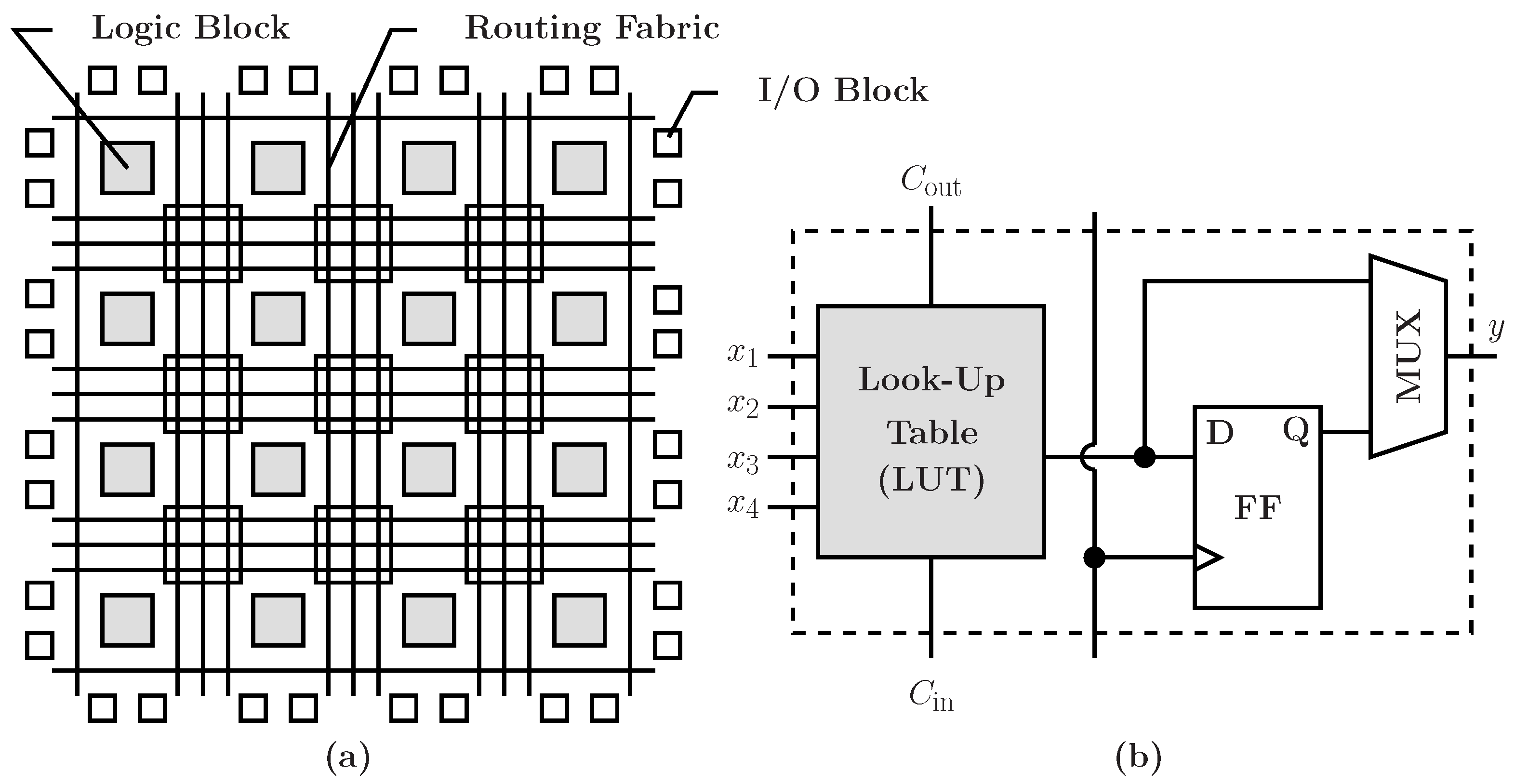
4. Modeling FPGA Device Aging
An FPGA is a logic device that contains a two-dimensional array of generic logic elements (LEs) and programmable switches, as shown in
Figure 7a. A logic element depicted in
Figure 7b can be configured (
i.e., programmed) to perform a simple function, and a programmable switch can be customized to provide interconnections among the logic elements. A custom design can be implemented by specifying the function of each logic element, selectively setting the connection of each logic element and selectively setting the connection of each programmable switch. A logic element usually contains a programmable look-up table (LUT), programmable interconnects and flip-flops (FF). An
n-input look-up table is typically implemented by a static random access memory (SRAM) and is used to implement any n-input combinational function. The flip-flops can be selectively used to implement sequential circuits. Most FPGA devices also embed certain macro cells, such as block RAMs, dedicated multipliers, clock managers and I/O interface circuits. Logic elements are usually grouped into logic array blocks (LABs). Since the LUT is the basic logic element to implement the logic function, in this work, we analytically quantify the aging-induced effect on the transistor for the FPGA reliability issue.
Figure 7.
(a) Sketch of the FPGA architecture; (b) diagram of a simple logic block. FF, flip-flop.
Figure 7.
(a) Sketch of the FPGA architecture; (b) diagram of a simple logic block. FF, flip-flop.
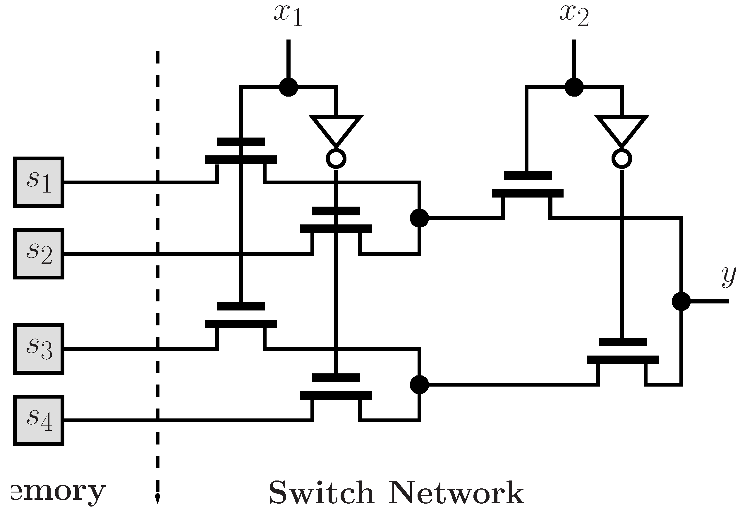
In FPGAs, LUTs are considered the basic blocks for mapping Boolean functions. Modern FPGAs allow modifications to the mapped function of LUTs through reconfiguration, partial or full, online or offline. The logic structure of a typical FPGA logic block consists of SRAM configuration bits and switching network.
Figure 8 depicts a small two-input LUT, whereas modern FPGA devices typically use six- or eight-input LUTs. In the following, we derive the error probability of a LUT analytically based on the error probability results of the SRAM cell and switching transistors developed in
Section 3.1 and
Section 3.2. Ideally, we should also incorporate flip-flops into our analytical framework. There are two reasons why we did not do that. First, this paper mainly focuses on the logic correctness of a placed and routed circuit implemented with an FPGA device. Flip-flops are clocked circuits whose outputs may change on an active edge of the clock signal based on its input. Flip-flops normally would not change the output upon input change, even when the clock signal is asserted. Therefore, the logic correctness of an FF mostly depends on the timing violations due to device aging, which can be more effectively addressed by reducing the clock rate or allowing more generous timing margins at the design stage. Secondly, for all combinational circuits, FF does not exist. Even for the sequential circuits, the number of FFs is much smaller than the number of switches in a modern FPGA. Finally, although we did not include FFs in our theoretical analysis, we include every gate in our experiments of extracting modular criticality through simulations.
Figure 8.
Logic diagram of a two-input LUT.
Figure 8.
Logic diagram of a two-input LUT.
4.1. Aging-Induced Effect on LUT-SRAM
As discussed in
Section 3, the device aging effect can cause read, write and hold failure in SRAM cells. In fact, the error probability of a SRAM cell is determined by
, which can be described as a function of device duration
t, technology node
and signal probability
α. Therefore, the error probability of a SRAM cell
.
After configuring an FPGA device, the SRAM cells in each of the activated LUTs store different logic values, “0” and “1”, that determine the functionality of each LUT, hence the overall functionality of the complete implemented logic design. During the operation of an FPGA device, for any given LUT used, different combinations of input signals will switch on different transistor paths. The switched-on path will establish the connection to a specific SRAM cell, whose stored logic bit becomes the output. Assume that the LUT has
N inputs; the total number of bits in the
N-LUT will be
. Furthermore, assume the access probability and the error probability of each SRAM cell to be
and
, respectively. Because the error probability of a memory cell also depends on its content [
21], we denote the error probability of a SRAM cell that stores “0” and “1” as
and
, respectively. Finally, we suppose that the error probability of each memory cell is totally independent. Therefore, the error probability of a
configuration memory block in a
N-LUT can be written as
. Now, we assume that all SRAM cells are designed and manufactured with the same error characteristics; therefore,
,
and
. As a result,
, where
and
denote the set of all memory cells that store “0” and “1”, respectively. Because the signal probability
α equals
, the final result:
As discussed in the previous section, the “1” cell is much more critical than the “0” cell, and the increasing of the signal probability of the LUT output for the “1” cell error probability will definitely increase the total probability of the SRAM.
4.2. Modeling Error Probability of Switching Network
As illustrated in
Figure 8, the LUT of modern FPGA devices typically uses an NMOS pass transistor as the switching elements. Different input signal combinations can turn on some of these switching transistors and route the bit content of one of LUT memory cell to the output
y. Therefore, the error probability for the switching network can be written as:
where and denote the probability of taking switching path i and the probability that the path i malfunctions.
A faulty switching path can be caused by the switching degradation of the NMOS transistor, as discussed in
Section 3.1. Fundamentally, the long stress time on the NMOS transistor may lead to increasing of threshold voltage
, which, in turn, results in degraded switching strength.
Figure 9 illustrates a switching path consisting of
N NMOS transistor switches. Assuming the aging-induced error probability of an individual NMOS transistor
to be
, the probability for the switching path to be faulty can be written as
, when
,
. Substituting this into Equation (
5) results in:
Figure 9.
One switched path containing N NMOSswitches.
Figure 9.
One switched path containing N NMOSswitches.
4.3. Analytically Modeling Error Probability in LUT
Each LUT in an FPGA device consists of two parts: the SRAM cell array and the multiplexer switching network. Assuming that these two components malfunction independently, the error probability of a LUT can be formalized as follows:
where
,
and
denote the error probability of a SRAM cell that stores “1” and “0” and the aging-induced error probability of an individual NMOS transistor (
M), respectively. Furthermore,
Because
, as discussed in
Section 4.1, obviously
, which means that the overall error probability of a LUT increases monotonically with the increase of the output signal probability
α. It will become clear that this result is critical in our optimal solution of improving the overall reliability of a placed and routed logic design with an FPGA device.
5. Analyzing FPGA Device Reliability
In this section, an intuitive approach to reliability analysis is described. It is based on the observation that a failure at a gate close to the primary output has a greater probability of propagating to the primary output than a gate several levels of logic away from the primary outputs. This is because a failure that has to propagate through several levels of logic has a higher probability of being logically masked. This can be quantified by applying the concept of observability, which has historically found use in the testing and logic synthesis domains.
In reliability analysis, the logic observability of any logic node can be defined as the probability that a logic value upset error (
or
) at the logic node under consideration will change the circuit outputs. As stated in [
22], logic observability can be computed with Boolean differences, symbolic techniques based on binary decision diagrams (BDDs) or simulation. In this study, we will attempt to derive a closed-form expression for the logic reliability,
, where
e denotes the error probability of each logic gate.
To the best of our knowledge, there has not been any systematic study on accurately measuring modular criticality values within a large-scale VLSI digital circuit. The most related works to this paper are several recent studies that explored various analytical ways of computing the overall logic reliability of VLSI logic circuits [
23,
24,
25,
26]. Reliability analysis of logic circuits refers to the problem of evaluating the effects of errors due to noise at individual transistors, gates or logic blocks on the outputs of the circuit. The models for noise range from the highly specific decomposition of the sources, e.g., single-event upsets, to highly abstract models that combine the effects of different failure mechanisms [
27,
28]. For example, in [
22], the authors developed an observability-based approach that can compute a closed-form expression for circuit reliability as a function of the failure probabilities and observability of the gates. Unfortunately, all of these analytical studies, although mathematically concise, have to make some key assumptions, therefore seriously limiting their applicability and accuracy. For example, the method in [
22] needs to approximate the multi-gate correlations in order to handle reconvergent fan-out. In addition, it is not clear how the existing analytical approaches can handle some unspecified probabilistic input vector distributions or more complicated correlation patterns within a VLSI logic circuit.
6. Optimally Improving Reliability via Discriminative Scaling
In a typical FPGA CAD flow, after logic synthesis and technology mapping, any given logic circuit will be converted into a network of LUTs (). Without loss of generality, we assume that the circuit under consideration consists of N LUTs, and each LUT has k inputs and one output. Furthermore, we assume that has M signal nets, each of which connects the output port of exactly one LUT to the input ports of a number of LUTs. Furthermore, we define the signal probability and error observability of signal net i as and , respectively. Finally, in this study, we define the product of and as the logic criticality of LUT i.
's output reliability is its probability of being correct in all its output ports when a large ensemble of identically and independently distributed (i.i.d.) random inputs are applied. Here, denotes the vector of error probability of all N gates.
Intuitively, the larger the is, the more critical the LUT i is to the correctness of the whole circuit . Note that the input vector distribution need not to be uniform i.i.d. Instead, it can be any general form. In other words, the larger the logic criticality is, the more sensitive the overall output reliability is towards LUT i's error.
The intuitive explanation of our definition of is straightforward. First, for any LUT i, represents the frequency of its output switching, which is directly related to the transistor aging and shows how likely a switching error will occur. Second, shows how sensitive the final output of will be to the output error of LUT i. Essentially, reflects the combined effect of both and towards 's overall correctness. In the following, we will show that our definition is not only intuitive, but also optimal in the sense that, using the ranking of logic criticality as the guidance, we can optimally maximize the overall reliability improvement of given a fixed amount of extra resources, such as additional chip area or extra power budget.
Thus, observability-based reliability analysis makes two simplifying assumptions for estimating the effect of multiple gate failures.
The effect of LUT failures at the primary output is decoupled from each other, i.e., a failure at each LUT i is assumed to affect the output with a probability regardless of other LUT failures. This assumption allows the joint observability to be replaced by simultaneous observability, which is computationally less demanding, to compute the effect of multiple gate failures at the output.
The observability of the LUTs are assumed to be independent of each other. Using this assumption, the computation of the simultaneous observability of two LUTs can be simplified to the product of the individual LUT observabilities. For instance, the probability that LUT 1 is observable and LUT 2 is not observable is given by , and the probability that LUT 1 and LUT 2 are both not observable is given by .
With this background, we shall derive the expression for the probability of error at the output for a general circuit network with N LUTs. Without loss of generality, we assume that the circuit has a single output y. Denote the error probability and logic observability of the ith LUT by and , respectively. Using the first assumption, the output y will be in error when an odd number of faulty LUTs in are simultaneously observable. Using the second assumption, the simultaneous observability of a set of LUTs can be computed by simply multiplying the individual observabilities of the LUTs.
In general, the probability that only the LUTs in
F are observable is given by
. The expression
has the same magnitude as
A and the same sign as
A when
F has an even number of LUTs and the opposite sign as
A when
F has an odd number of LUTs. Thus, when
F has an odd number of LUTs, the expression
gives the probability that the LUTs in F are observable, and when F has an even number of LUTs,
is equal to zero. Thus, the probability that an odd number of LUTs in
is observable is given by:
By the first simplifying assumption, the probability of error at the output y given that the LUTs in have failed is also given. Thus, .
The probability that the LUTs in
are in error and the LUTs in
are error-free is given by
. Thus, the probability of error at the output
y is given by
. Finally,
This result clearly shows that, in order to minimize the overall error probability , we should always choose the largest terms to remove. Therefore, given N LUTs in an FPGA design, if only K of them can be fortified, in order to maximize the overall design reliability, we should always choose the K LUTs with the largest criticality values , where .
7. Results and Analysis
To validate our error probability model and our discriminative assignment strategy, we have chosen 10 circuits from the Altera benchmark suite of the Quartus University Interface Program (QUIP). The overall procedure of our experiments is depicted in
Figure 10. All of our test circuits are in the form of Verilog source files. We rely on the commercial Altera Quartus 2 software to perform all FPGA logic synthesis, logic optimization and technology mapping. Finally, the resulting .QVM files from the Quartus contain both the LUT netlist and the encoded logic truth table for each LUT. We then use our in-house logic simulation tools to read in the .QVM file, and perform logic simulation. As in many other studies, we use extensive Monte Carlo logic simulation to obtain the error probability of any given circuit design. For each benchmark circuit, we cover all possible input combinations. For each input combination, we run many simulation iterations in order to obtain accurate output reliability. Of course, the number of simulation iterations for any given input vector will highly depend on the specific topology and complexity of the targeted logic circuit. We continue logic simulations until the out error probability saturates. Our results have shown that typically 5,000 logic simulations for each input vector are often sufficient. As for logic observability, we use a similar approach, the only difference being that we only invert the logic value at the logic node under consideration, while keeping all logic values at all other nodes unchanged. The observability will be measured by counting the probability for any output to change its value. Obviously, these measurement results also take the dependency of logic observability on internal logic values into considerations. To deal with the intensive computations required for the above logic simulations, we employ the STOKEScomputing cluster at UCF (University of Central Florida), which consists of 3,450 compute cores (Intel Xeon 64-bit processors) and over 7.5 TB of RAM. The total simulation took about one week to complete.
We use the 45-nm predictive technology model (PTM) to model all CMOS devices (
http://ptm.asu.edu). At the nominal
and
, we assume the error probability of all transistors to be zero. We then set the on-time to be
years and obtain the duty cycle values
Y from our logic simulations. Next, using Equation (
1), we compute the
, which can then be used to obtain
using Equation (
2). Using Equation (
3), we then obtain the error probability of a single transistor
. Finally, we can calculate the error probability of any single LUT by the method discussed in
Section 4. Note that the above methodology of computing error probability caused by device aging is only applicable to pass-transistor switches. Because the SRAM elements store constant values, we use a different approach to evaluate the aging effect on the error probability. Specifically, as discussed in
Section 4.1, after obtaining
using Equation (
2), we can utilize the empirically-measured data, as shown in
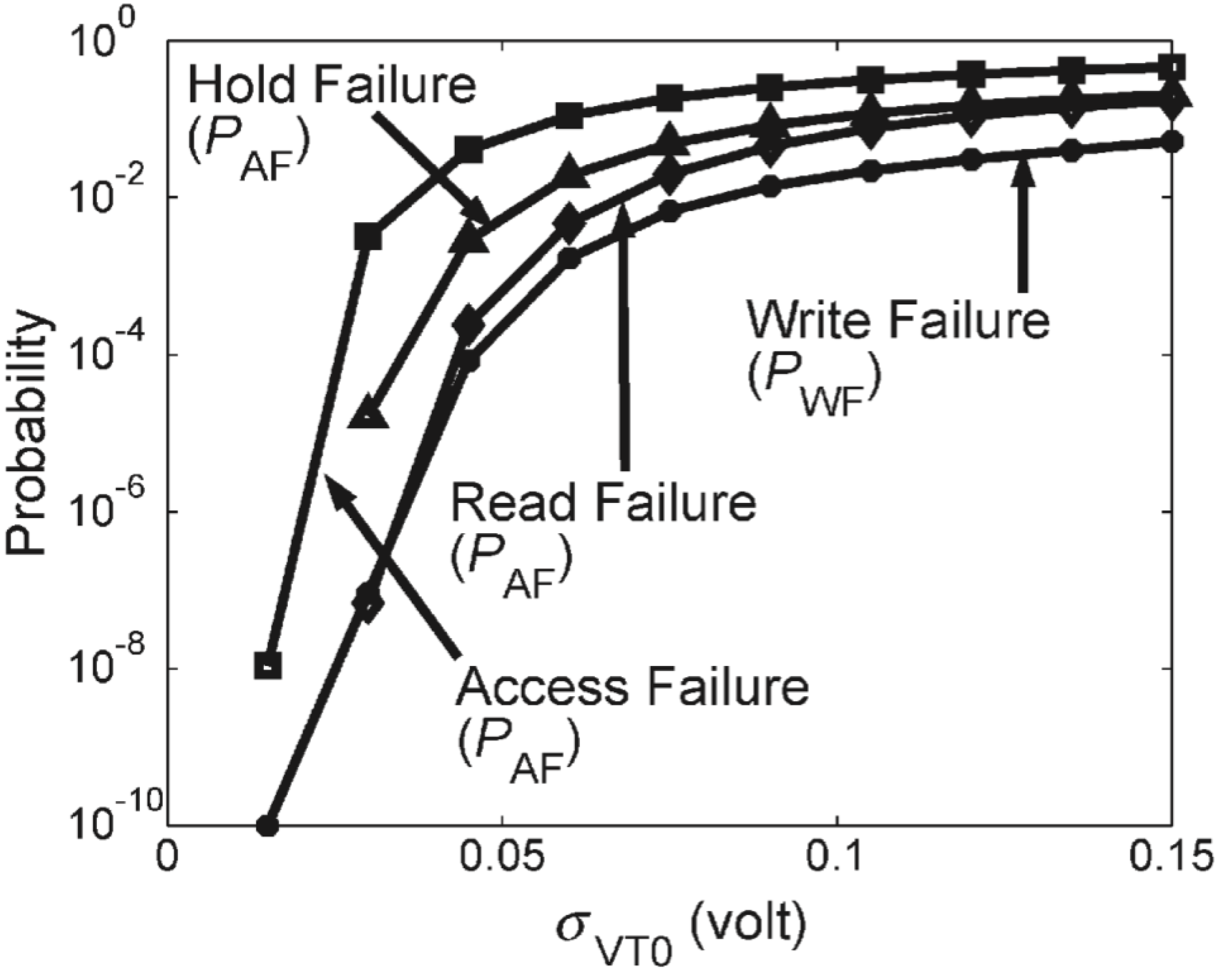
Figure 6, to read out three main components of the error probability of a SRAM memory cell [
21], which can be readily combined to obtain the total memory error probability due to device aging. Our results have shown that for the 45-nm CMOS technology, after three years of switch-on time, the
is 0.063 V, which induces about
in LUT error probability. This error probability can be completely eliminated by elevating the
to be about 1.1 V.
Figure 10.
CAD flow of our circuit design experiments.
Figure 10.
CAD flow of our circuit design experiments.
All results in
Table 1 have been obtained under the above assumptions. For each of these ten benchmarks, we conduct four sets of experiments denoted by U, A, B and C. Type U experiments serve as the baseline when no circuit fortification is done. In Type A experiments, we use the optimal fortification strategy that we developed in
Section 6,
i.e., we chose
K LUTs with the largest criticality values to fortify. In Type B experiments, we randomly pick
K LUTs to fortify, while in Type C experiments, we do the opposite to our optimal fortification strategy: we chose
K LUTs with the smallest criticality values to fortify. Finally, we have tried three different
K values, which are 10%, 20% and 30% of
N.
Table 1.
Results of the overall error probability for all 10 Quartus University Interface Program (QUIP) benchmarks.
Table 1.
Results of the overall error probability for all 10 Quartus University Interface Program (QUIP) benchmarks.
| | LE# | PIN# | U | top 10% | top 20% | top 30% |
|---|
| A | B | C | A | B | C | A | B | C |
|---|
| OC_SRAM | 243 | 153 | 0.0387 | 0.01046 | 0.0265 | 0.02636 | 0.00331 | 0.00887 | 0.008812 | 0.00331 | 0.00887 | 0.008812 |
| B04 | 189 | 21 | 0.03698 | 0.01581 | 0.0276 | 0.0281 | 0.00404 | 0.00843 | 0.008139 | 0.0016 | 0.002811 | 0.002711 |
| Barrel16 | 135 | 38 | 0.0314 | 0.01314 | 0.0192 | 0.0198 | 0.00361 | 0.00714 | 0.007108 | 0.00105 | 0.00295 | 0.003071 |
| Barrel64 | 897 | 136 | 0.1765 | 0.03023 | 0.1274 | 0.1211 | 0.00841 | 0.0231 | 0.02341 | 0.000817 | 0.00714 | 0.007131 |
| EX1010 | 871 | 20 | 0.145 | 0.0912 | 0.1287 | 0.1233 | 0.045 | 0.0854 | 0.0844 | 0.01226 | 0.0368 | 0.03067 |
| FLIP_RISK8 | 1490 | 113 | 0.282 | 0.0876 | 0.235 | 0.2345 | 0.0484 | 0.085 | 0.082 | 0.0106 | 0.021 | 0.024 |
| MUX8_64 | 835 | 76 | 0.161 | 0.054 | 0.112 | 0.116 | 0.0114 | 0.0877 | 0.0881 | 0.006325 | 0.00969 | 0.00971 |
| OC_AES_CORE | 5005 | 388 | 0.312 | 0.082 | 0.278 | 0.277 | 0.01087 | 0.051 | 0.0526 | 0.0081 | 0.0314 | 0.0322 |
| OC_FPU | 6972 | 110 | 0.351 | 0.0754 | 0.2588 | 0.257 | 0.012745 | 0.0621 | 0.0652 | 0.006124 | 0.00881 | 0.00892 |
| OC_DES3PERF | 20188 | 298 | 0.413 | 0.0959 | 0.381 | 0.3815 | 0.010745 | 0.07821 | 0.07813 | 0.00196 | 0.009181 | 0.00912 |
As shown in
Table 1, for all benchmark circuits, our optimal discriminative voltage scaling method has significantly improved its overall logic circuit reliability. The improvement ranges from approximately three-times to five-times. Not surprisingly, the opposite voltage scaling (Type C) has performed poorly with reliability improvements ranging from merely 10% to 30% for
. Also intuitively true, when
K values increases from 10% to 30%, for any benchmark circuit and any voltage scaling method, the improvement in overall circuit reliability steadily increases. Somewhat surprisingly, when comparing Type B with Type C experiments, very few differences can be found. This essentially shows that, without utilizing the LUT criticality values as the guidance for discriminative voltage scaling, the reliability improvement is almost as poor as the worst scenario. This finding clearly shows the significant advantage of our proposed discriminative voltage scaling scheme based on the LUT criticality ranking.
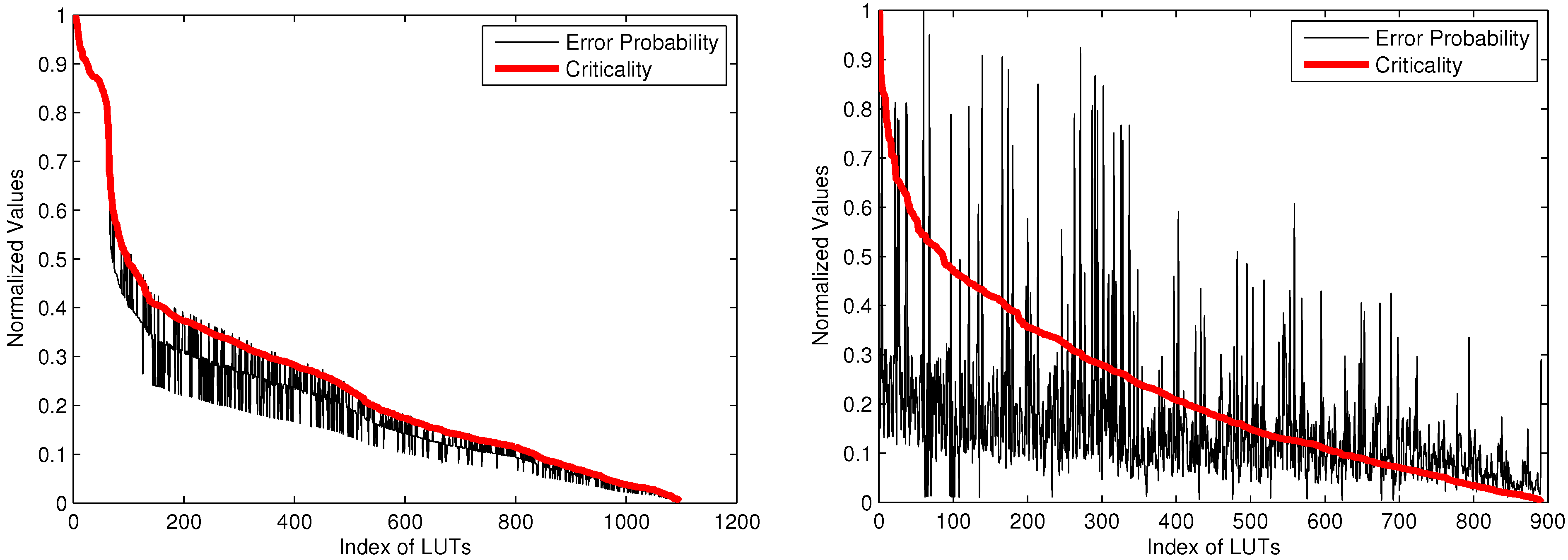
When examining the results in
Table 1 more carefully, one can find that the effectiveness of our discriminative voltage scaling method varies widely. For example, after fortification, the reliability of
has been improved by almost 3.22-times, while the reliability of
has only been improved by 1.58-times, although both circuits are of almost the same size. To better understand this phenomenon, in
Figure 11, we have plotted the value profile of LUT criticality and LUT error probability values for both circuits. In each circuit, we first sort all of the LUTs according to the decreasing order of criticality. We then plot the LUT error probability values according to this sorted order. Comparing
Figure 11a,b, one can easily observe that for the circuit
, the sorting order of LUT criticality and error probability match quite closely. In contrast, for
, these two orderings differ greatly. In other words, for
, the most critical LUT often is the one with the highest error probability, while for
, the opposite is true. Therefore, in the case of
, we may have fortified many LUTs with very low error probability, hence the relatively low effectiveness of our discriminative voltage scaling.
Figure 11.
Profile comparison between LUT criticality and LUT error probability values. (a) Results of circuit FLIP_RISKS. (b) Results of circuit Ex1010.
Figure 11.
Profile comparison between LUT criticality and LUT error probability values. (a) Results of circuit FLIP_RISKS. (b) Results of circuit Ex1010.
8. Related Work
Criticality analysis has been extensively studied in software [
29], but is quite rare in error-resilient computing device research. Only recently, the general area of criticality analysis (CA), which provides relative measures of significance for the effects of individual components on the overall correctness of system operation, has been investigated in digital circuit design. For example, in [
30], a novel approach to optimize digital integrated circuit yield with regards to speed and area/power for aggressive scaling technologies is presented. The technique is intended to reduce the effects of intra-die variations using redundancy applied only on critical parts of the circuit. In [
31], the researchers have explored the idea of discriminatively fortifying a large H.264 circuit design with FPGA fabric. They recognize that: (1) different system components contribute differently to the overall correctness of a target application and therefore should be treated distinctively; and (2) abundant error resilience exists inherently in many practical algorithms, such as signal processing, visual perception and artificial learning. Such error resilience can be significantly improved with effective hardware support. However, in [
31], the authors used Monte Carlo-based fault injection, and therefore, the resulting algorithm cannot be efficiently applied to large-scale circuits. Furthermore, their definition of modular criticality was quite
ad hoc, therefore lacking analytical justification.
More relevant to our study, [
32] introduced a logic-level soft error mitigation methodology for combinational circuits. Their key idea is to exploit the existence of logic implications in a design and to selectively add pertinent functionally redundant wires to the circuit. They have demonstrated that the addition of functionally redundant wires reduces the probability that a single-event transient (SET) error will reach a primary output and, by extension, the soft error rate (SER) of the circuit. Obviously, the proposed circuit techniques can be readily applied using our proposed criticality estimation method, especially in a large-scale circuit case. However, more importantly, the method used in [
32] to determine circuit criticality is mostly done by assessing the SET sensitization probability reduction achieved by candidate functionally-redundant wires and selects an appropriate subset that, when added to the design, minimizes its SER. Consequently, their overall method of criticality analysis is rather heuristic and utilizes largely “local” information. In addition, it is not very clear how this method can scale with very large-scale circuits.
Samudrala
et al. [
33] also targeted hardening combinational circuits, but focused on mapping digital designs onto Xilinx Virtex FPGAs against single-event upsets (SEUs). They do not perform detailed criticality analysis. Instead, their method uses the signal probabilities of the lines to detect SEU-sensitive sub-circuits of a given combinational circuit. Afterwards, the circuit components deemed to be sensitive are hardened against SEUs by selectively applying triple modular redundancy (STMR) to these sensitive sub-circuits. More recently, in [
34], a new methodology to insert selective TMR automatically for SEU mitigation has been presented. Again, the criticality was determined based on empirical data. Because the overall method is cast as a multi-variable optimization problem, it is not clear how this method can scale with circuit size, and few insights will be provided as to which part of the circuit is more critical than others, and by how much.
Finally, another related study [
6] also studied the transistor aging mostly due to NBTI and PBTI for FPGA technology. However, they only investigated the effect of transistor aging, due to NBTI and PBTI, in LUTs, by considering different implementations through detailed SPICE simulations. In contrast, our study involves both analytical and empirical studies. More importantly, we study how to improve the overall logic reliability for logic circuits implemented with an FPGA device, without modifying any logic structure in FPGA circuit implementations. Our main approach is to strategically elevate
at various critical components to maximize its reliability benefits.


