1. Introduction
The DC power converter is an essential element for effective power generation and management systems, such as the DC micro grid, renewable power generation system, and energy storage systems [
1,
2,
3,
4]. Analysis and design of efficient and stable power converters have been studied widely [
5,
6,
7]. Depending on the power source and load conditions, three basic converters; buck (step-down), boost (step-up), and buck-boost converters are available for particular applications.
The buck-boost power converter is capable of converting the source voltage to higher or lower voltages to the load terminal. High speed power MOSFETs switches are usually employed to control the energy flow from the supply to the load terminal. A desired output voltage can be achieved through properly control of the duty cycle for the power switches. However, given the voltage variations in the input, control of the power switch, driver circuit design for the MOSFET, stability for the small signal perturbation, and over current protection, etc., the design of the buck-boost controller is challenging and complicated. Thanks to the demands of industry, high efficiency power converter controllers such as LTC3780 [
8], TPS40057 [
9], TPS40200 [
10], etc., are available for the designer. With these controllers, voltage regulation is easily achieved using simple voltage-divider networks. Once the voltage-divider network is selected, the output voltage of the power converter is maintained at the predetermined level despite the voltage variation at the input terminal. However, if a variable output voltage is required for specific performance and applications, an additional control circuit has to be included to provide the auto-ranging function.
In the current study, we focused on the design of an auto-ranging buck-boost power converter system for unmanned aerial vehicle (UAV) power management application. The system contains two major subsystems, namely, a Zeta type buck-boost power converter and a control unit. The function of the system is divided into two control loops. The inner-loop is a voltage regulator based on a Zeta type buck-boost converter. The outer-loop is for voltage and current regulation. The voltage/current regulation is achieved through controlling a light dependent resistor (LDR) based variable voltage-divider from the control unit. An LDR is a type of resistor whose resistance varies depending on the amount of light falling on its surface. It can be used in a circuit where it is required to sense the presence of light [
11,
12]. The LDR based variable voltage-divider provides contactless and continuous means for auto-ranging voltage and current regulation. Details of the design are given in
Section 2.
Section 3 presents a microcontroller controlled buck-boost power converter based on the proposed method. Computer simulations based on a MATLAB/SIMULINK model were successfully conducted to verify the design. In addition, a prototype system was built and successfully tested for Li-ion battery charging application. Results of the battery charging testing are provided in
Section 4. The conclusions of the study are summarized in
Section 5.
2. Buck-Boost Power Converter
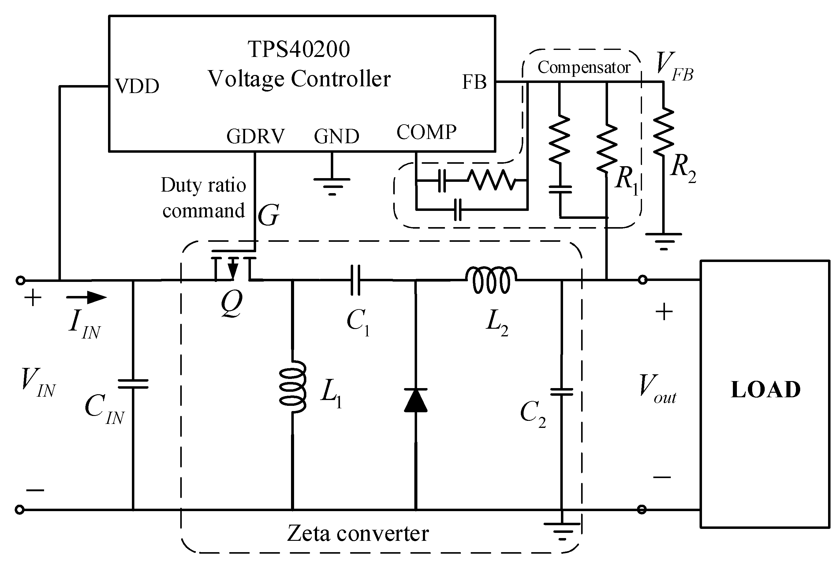
The buck-boost converter considered in this design is a Zeta type converter as shown in
Figure 1. A high-speed p-type power MOSFET (
in
Figure 1) was employed to control the energy flow and voltage regulation. An example of the TPS40200-based Zeta type buck-boost DC to DC power converter is shown in
Figure 2.
The output voltage
in
Figure 2 is maintained by regulating the feedback voltage,
, of the
formed voltage divider as shown in
Figure 2. The voltage
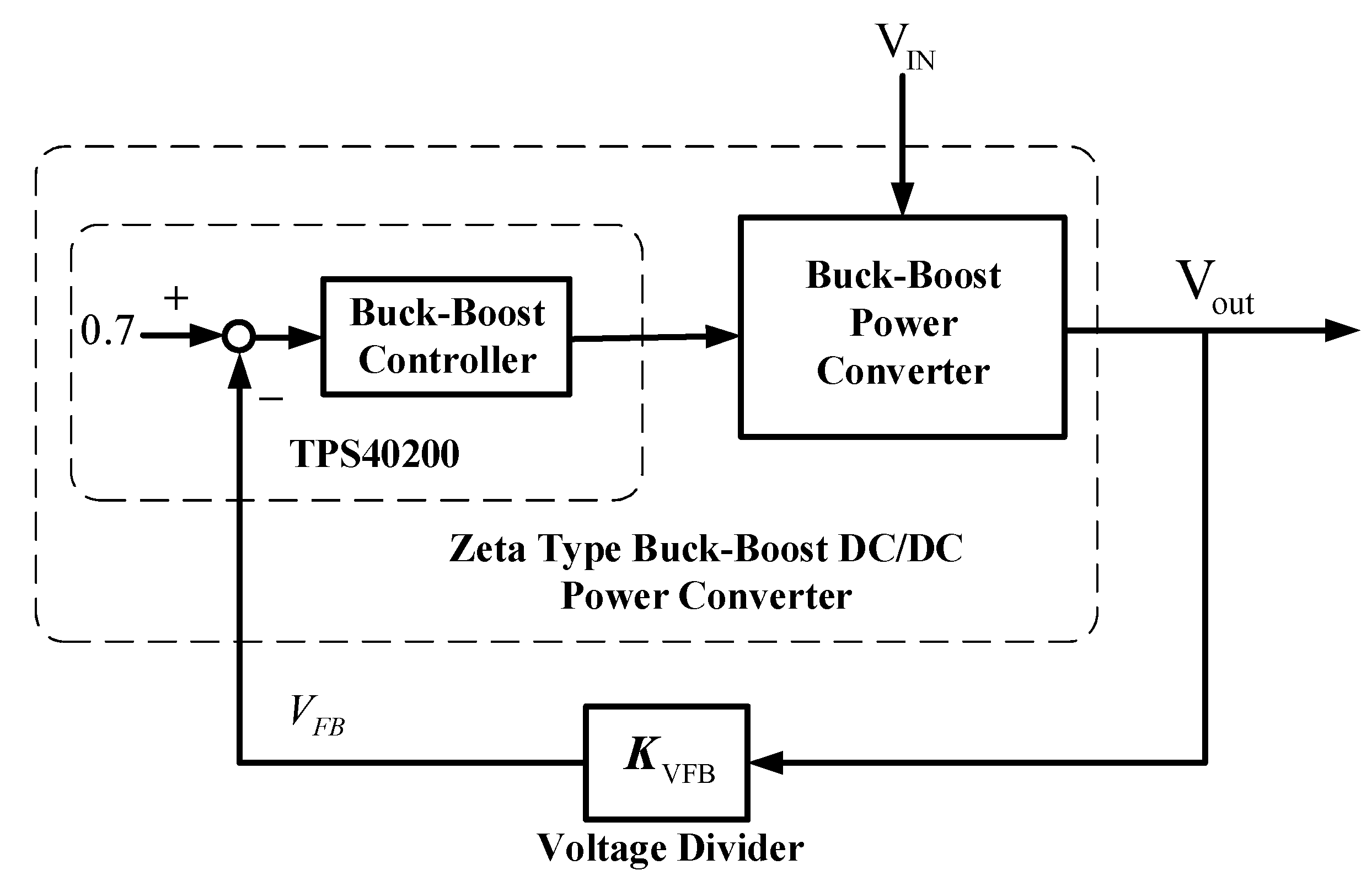
is regulated at 0.7 V by a feedback control loop in the TPS40200 voltage regulator as depicted in
Figure 3. The voltage feedback gain
in
Figure 3 is a voltage divider formed by
. That is
Thus, the output voltage is maintained at
Obviously, output voltage
is determined by proper selection of
. To simplify the design, we fixed the resistance
so that
becomes the only variable to control. For example, if we want to control output
to vary from +5 V ~ +30 V, we need to control
to vary from
to
if
is
. The remaining problem becomes how to control the resistance
so that the desired
is achieved. This implies that
must be some form of variable resistor that can be controlled easily. Due to the high-speed switching control of the MOSFETs, a power up problem is inherent in the system if a variable resistor is used directly for
. The problem is that we have to set
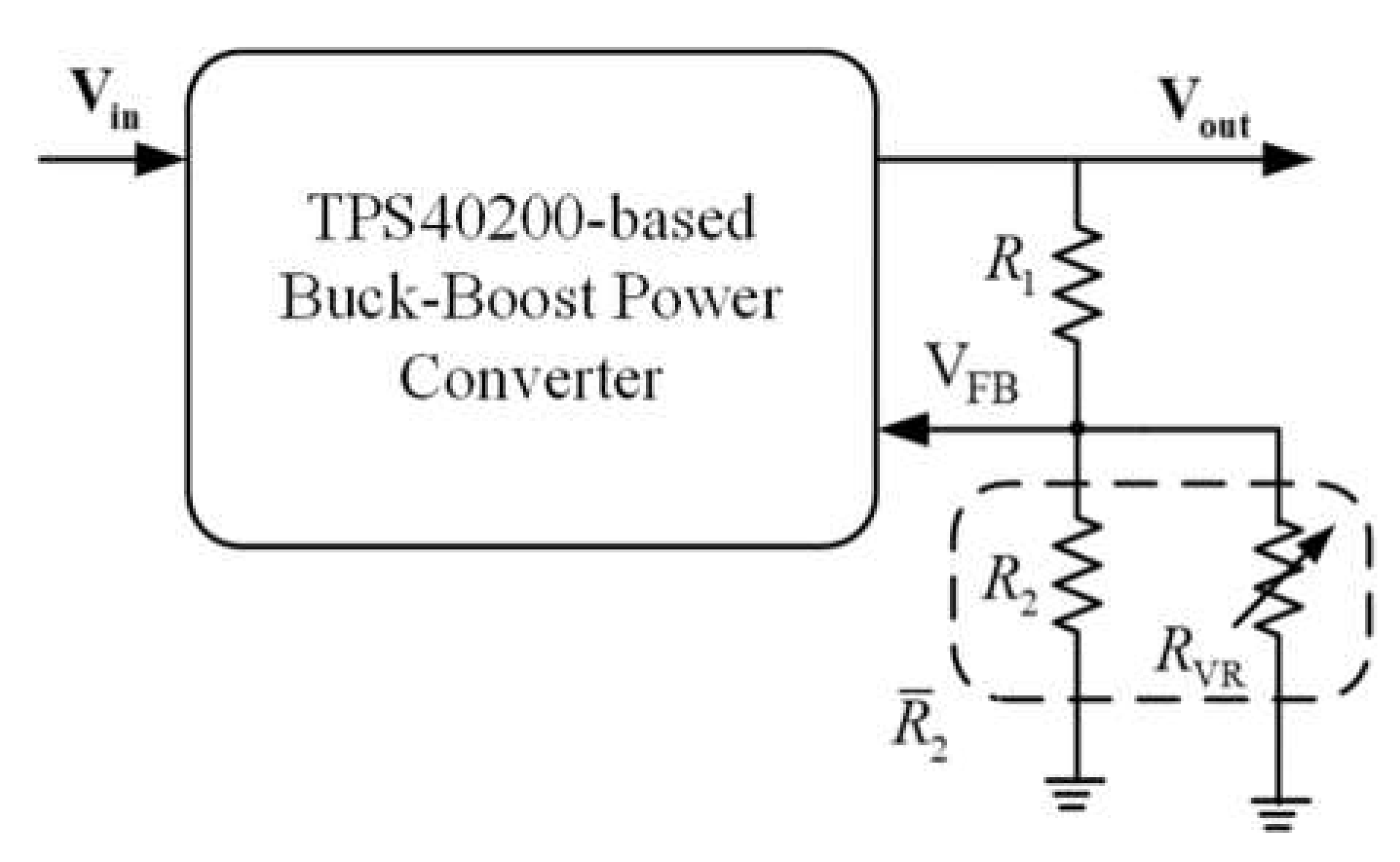
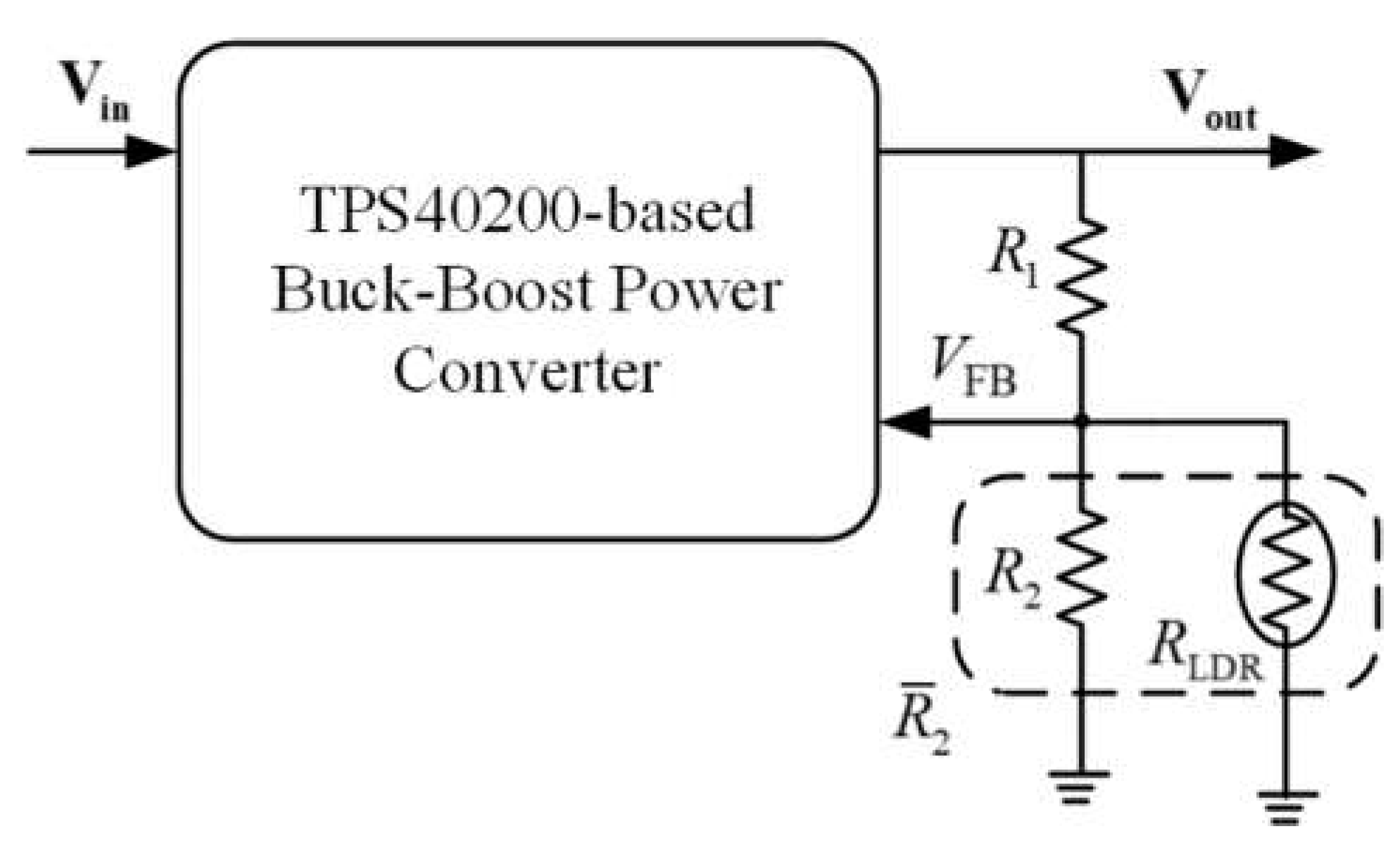
to a proper value before we power up the buck-boost converter otherwise the converter fails to operate or even burns out. To avoid these problems, we used a fixed resistance
in parallel with a controlled variable resistor to perform voltage regulation. Two types of variable resistors are discussed in this design as shown in
Figure 4 and
Figure 5.
Figure 4 is the configuration using a digital variable resistor.
Figure 5 shows the configuration using a LDR to perform the required function. The drawback of using a digital variable resistor is that it is a contact type resistor with discontinuous changes in the resistance. It creates more unwanted noises in the control process. Furthermore, depending on the resolution of the digital resistor (8 bits and 10 bits are common in the industry) the output voltage is limited to certain steps and easily leads to limit-cycle phenomenon. The LDR based variable resistor provides contactless, continuous changes in its resistance,
, according to the light intensity falling on it. Depending on the type and materials used, the resistance
can be as low as
to
when fully illuminated and as high as
(dark resistance) when in dark conditions.
In (3)
represents the minimal voltage that appears at the output terminal when the LDR is left uncontrolled (dark resistance). Increasing the light intensity on the LDR decreases the resistance
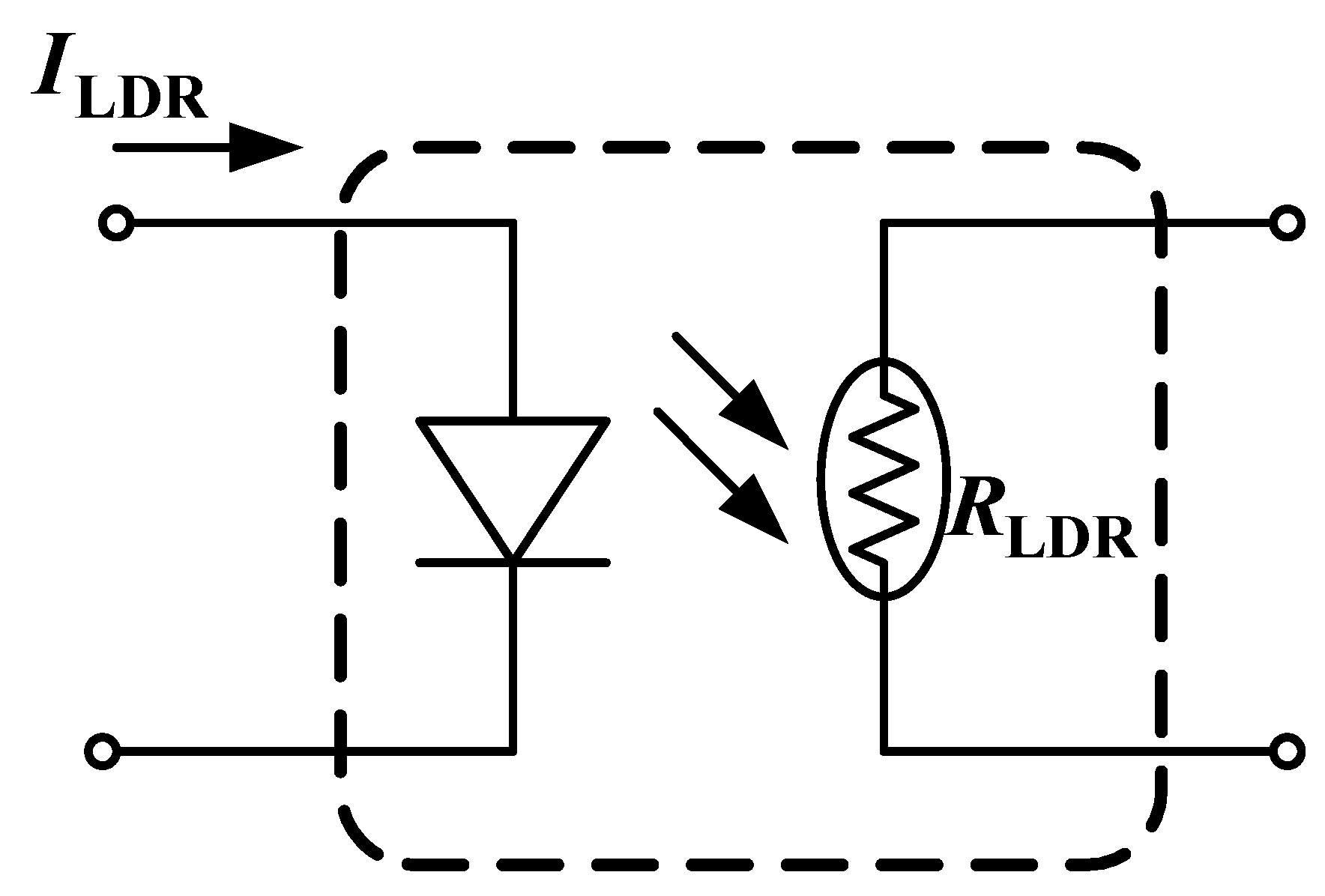
. Thus, the output voltage increases as light intensity on the LDR increases. The LDR and LED integrated device is commercially available [
13] for light intensity control of the LDR, as shown in
Figure 6. Light intensity is controlled by commanding the current,
through the LED, which in turn will change the resistance
.
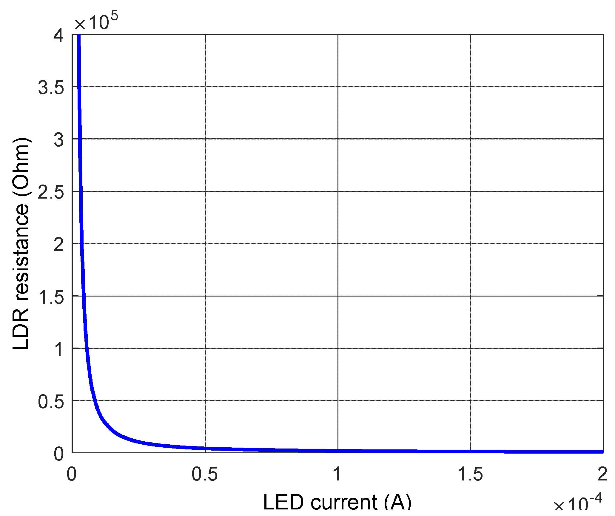
An experiment was conducted to examine the quantitative properties of the LDR. The resistances
at different LED currents are shown in
Figure 7. It shows the nonlinear phenomenon between the LDR resistance and the applied current. However, the properties might differ slightly from part to part.
Using curve fitting, the experimental data was expressed by the following
From the characteristics of the LDR, as shown in
Figure 7, the sensitivity of
with respect to LED current is significant in small current region (high
region). Compared to the low resistance region, the contribution to output voltage changes is less significant in the high resistance region. Moreover, control of low LED current is less reliable and impractical. Therefore, a low resistance region was selected for the buck-boost converter design in this study.
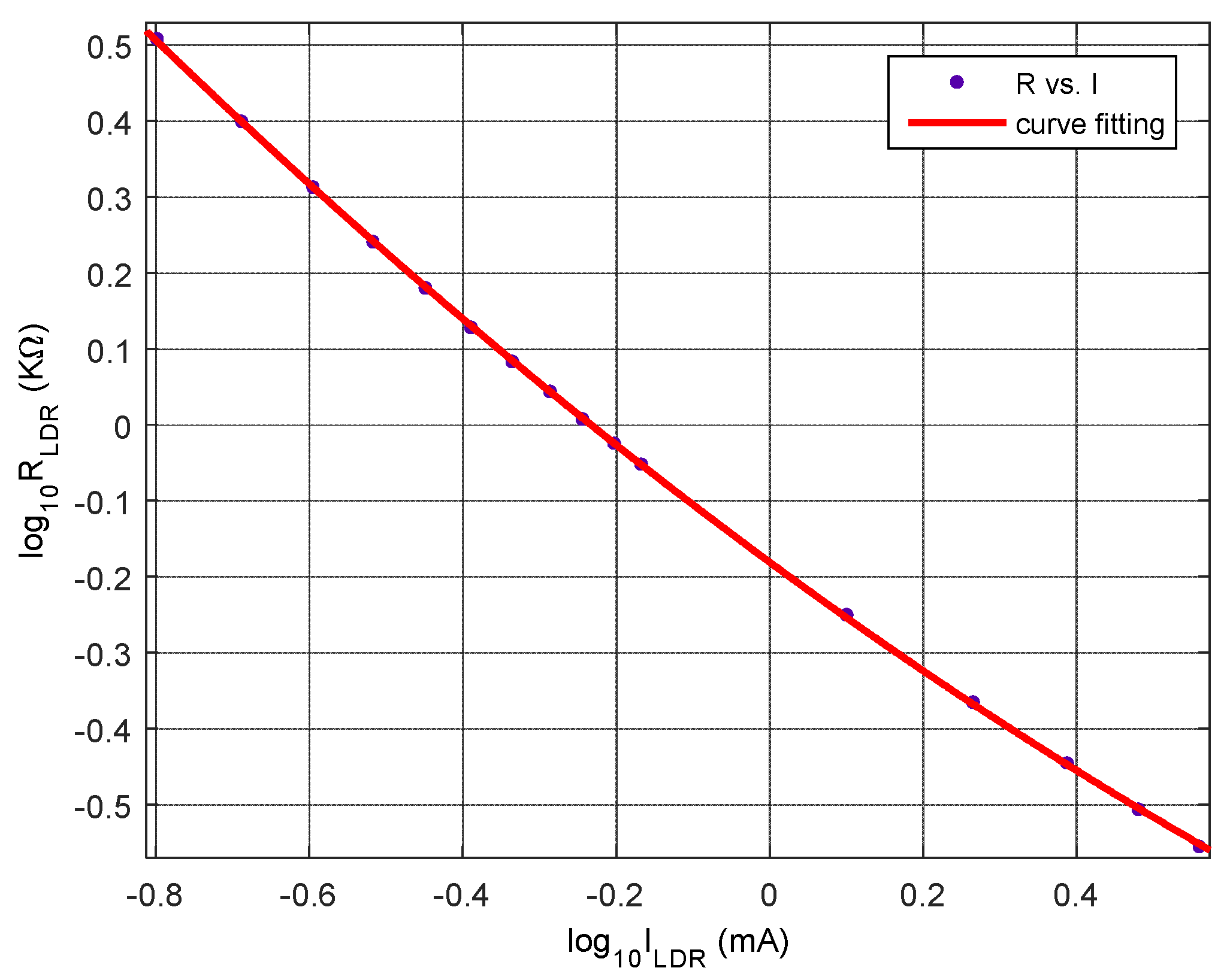
Figure 8 represents the comparison of test data and curve fitting results for
in
region. This region is selected in response to the design requirement that is set in this research.
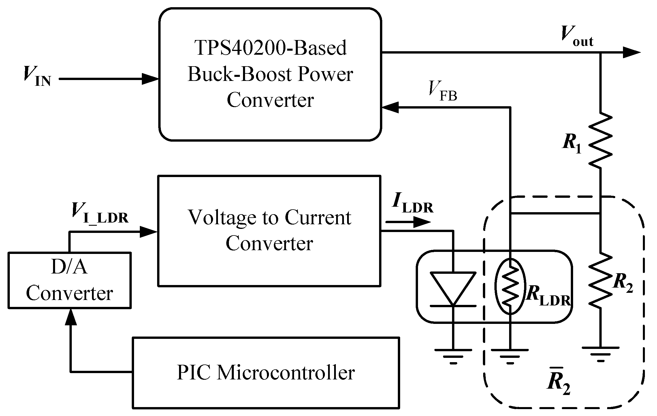
The characteristics of the LDR and its defined control region, the open-loop system of the LDR control, is presented in
Figure 9. A voltage to current converter is incorporated in the system to convert the command from the microcontroller to LED demanded current.
Figure 2 shows voltage regulation using a Zeta type buck-boost power converter. If the resistors
and
are fixed, the output voltage will be regulated to a fixed level.
Figure 3 represents the voltage regulation in the feedback control loop and can be used for further analysis.
Figure 9 shows the schematic diagram for control of the LDR resistance. The output voltage level can then be controlled via control of the LDR resistance.
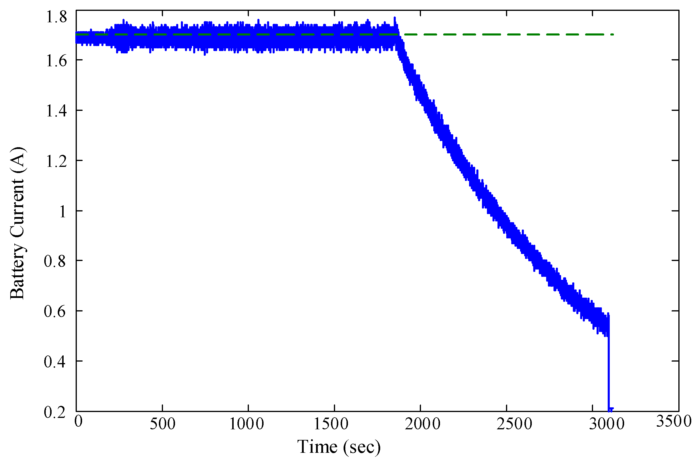
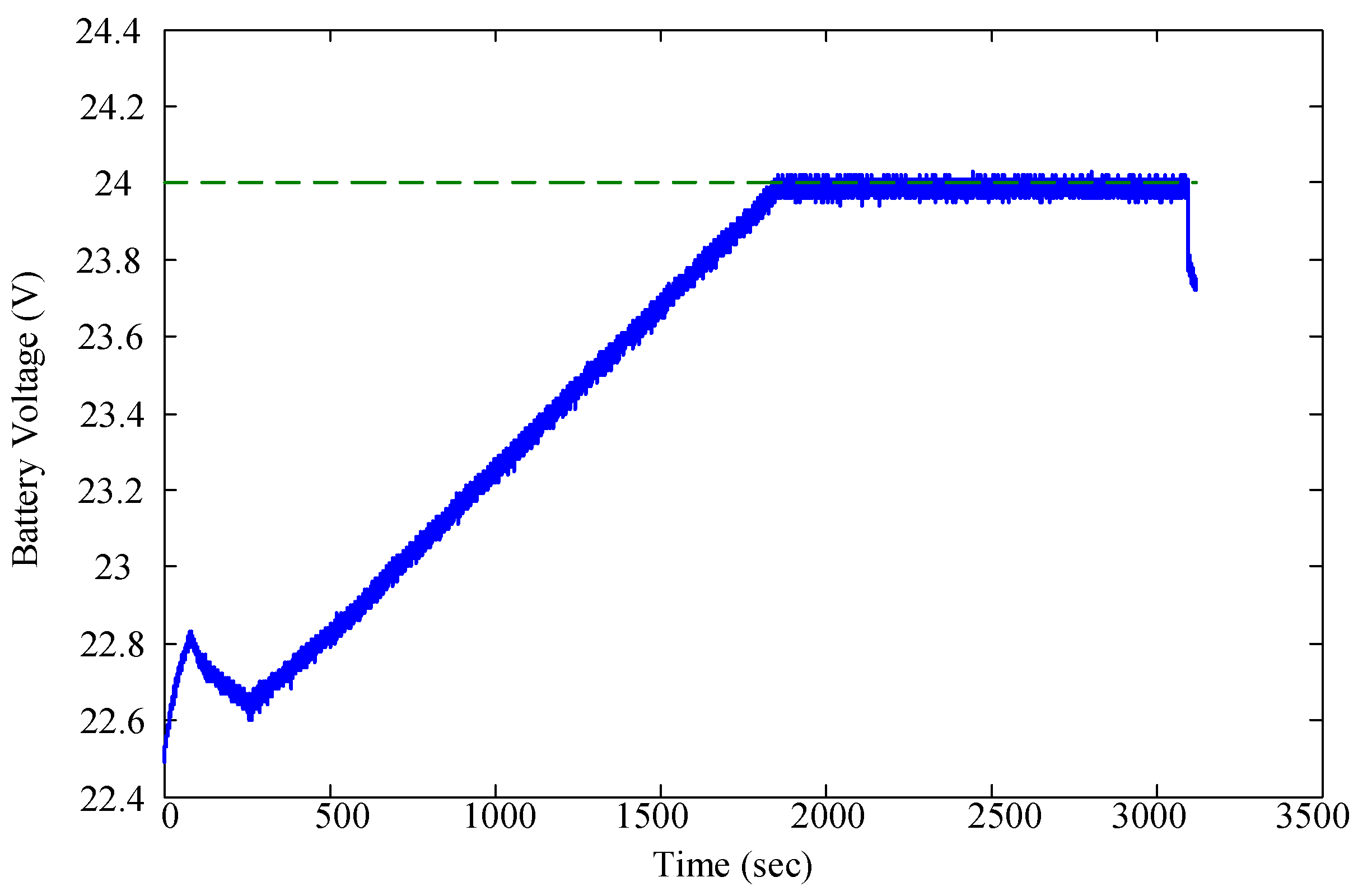
The goal of this research was to design a microcontroller controlled auto-ranging buck-boost power converter for the power management system of an experimental solar-powered UAV. The maximum power point for the PV array used for the UAV was about 24 V at irradiation of 1000 W/m
2. For battery charging, the goal was to provide the capability for charging battery modules with either 3 cells or 6 cells connected in series. The charging process includes constant current and constant voltage mechanisms. The required output voltage for 3 cells module is around 10–12.6 V and 20–25.2 V for 6 cells module. The voltage required for the propulsion system is 26 V for the UAV. Conservatively, the range of output voltage was set to be controlled between 5 to 30 V, which covers the design requirements to initiate the design. The resistances
, and
were selected to achieve
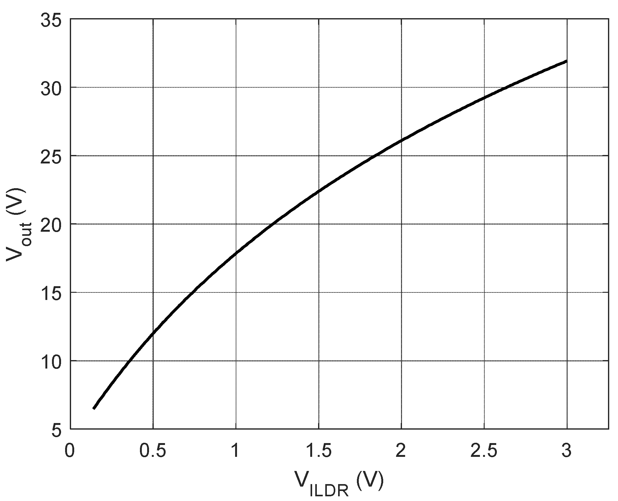
. When 1.5 mA LED current is applied to the LDR, the corresponding
resistance is
which will produce +31.89 V output voltage. The command from the microcontroller was selected to be 0–5 V. The gain for the voltage to current converter was chosen as 2.5/5 (mA/V). The range of
we chose for the design was from
to
. The corresponding LED current was from 0.07 mA to 1.5 mA. Thus, the range of the voltage command was from 0.035 V to 3.0 V. This produces controlled output voltage between
, which satisfies the design requirements. The relationship between the output voltage and the command from control unit is shown in
Figure 10. Voltages less than 6.49 V are not considered to be as precise as the selected controlled region.
3. Microcontroller Controlled Buck-Boost Power Converter
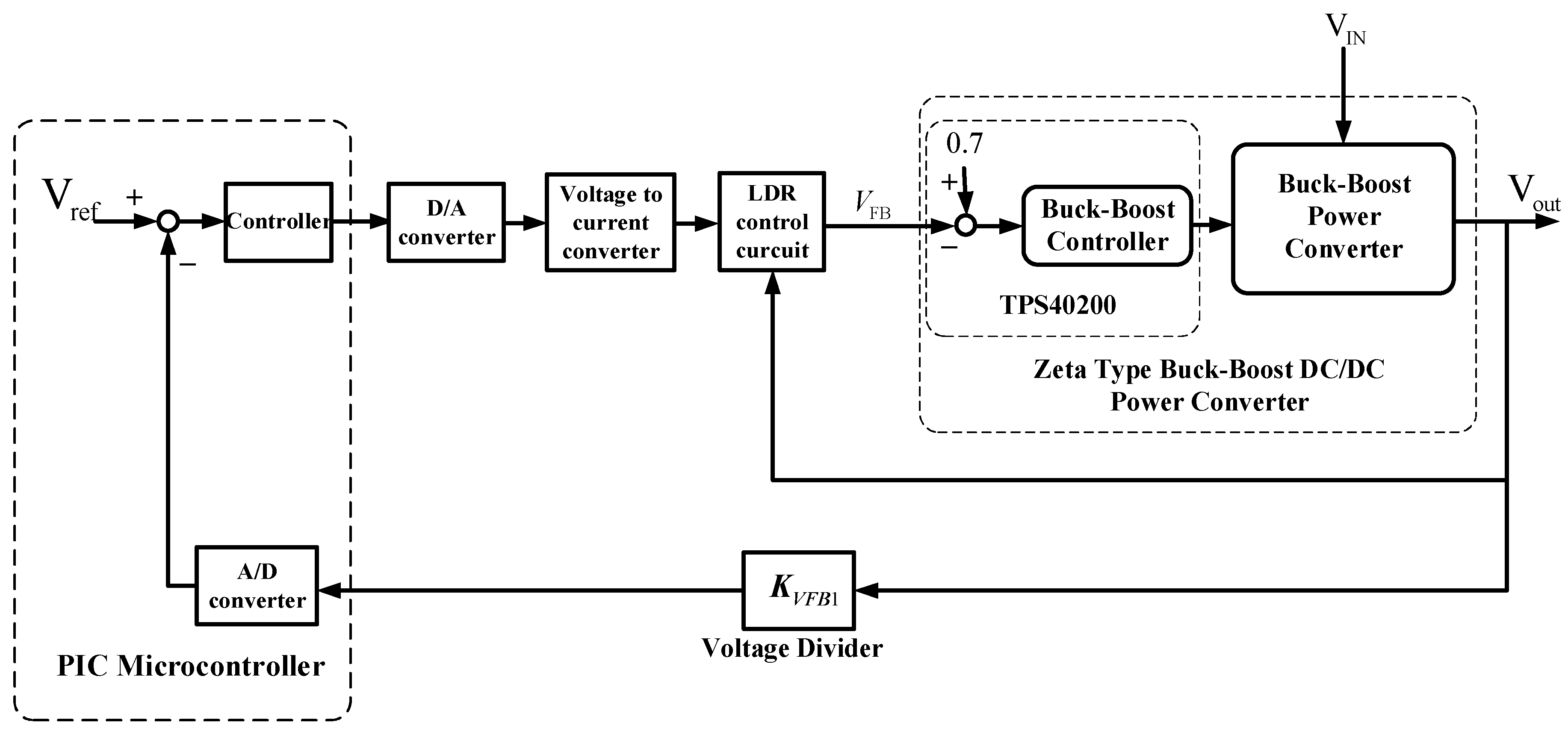
A feedback control system was constructed as shown in
Figure 11 to proceed to the control system design. The system contains two control loops. The inner-loop is a voltage regulator based on a Zeta type buck-boost converter. The outer-loop is for the auto-ranging buck-boost power converter. The voltage divider
in the outer loop of
Figure 11 is used for scaling down the output voltage for the A/D converter. A type III compensator [
14] to provide an unconditionally stable loop is employed for the inner-loop. The auto-ranging control loop is accomplished through the control of an LDR installed in between the Zeta converter and the load using a fuzzy-logic based controller.
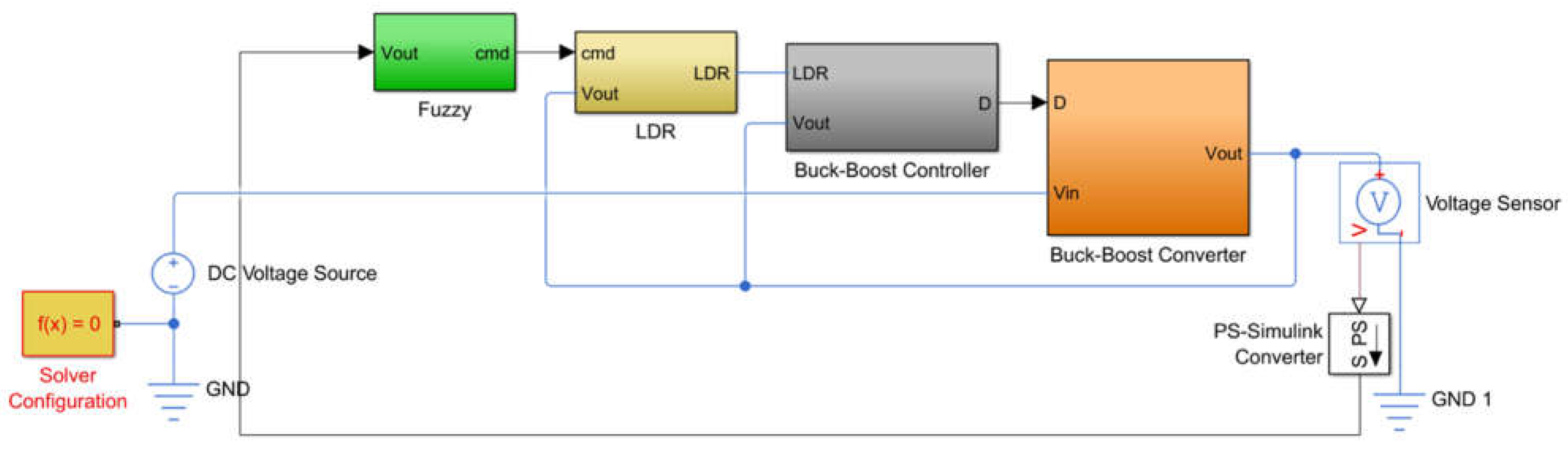
Based on the characteristics of the LDR, the Zeta converter, and the proposed feedback control system, a MATLAB/SIMULINK based circuit simulation model for the auto-ranging DC-to-DC power converting system was developed as shown in
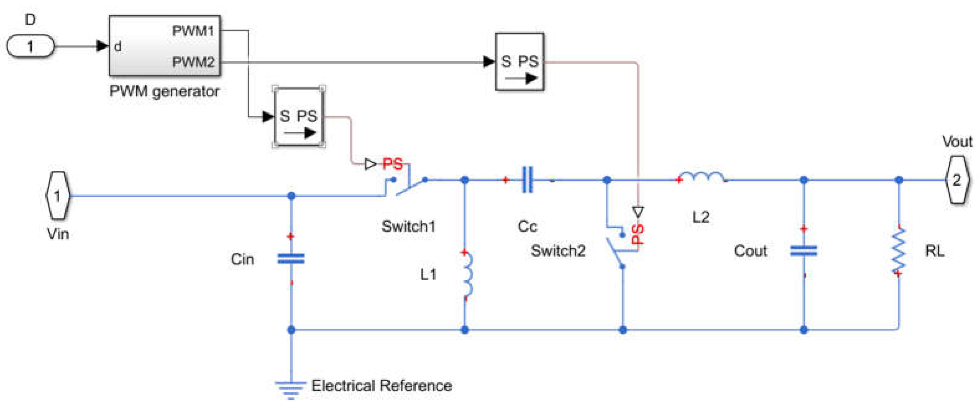
Figure 12. The simulation model mainly consists of a Zeta type buck-boost converter model, a Type III compensator based buck-boost controller, an LDR circuit model, and a fuzzy logic controller. Details of the Zeta type buck-boost converter model are shown in
Figure 13. The Type III compensator based buck-boost controller for inner-loop voltage regulation is shown in
Figure 14.
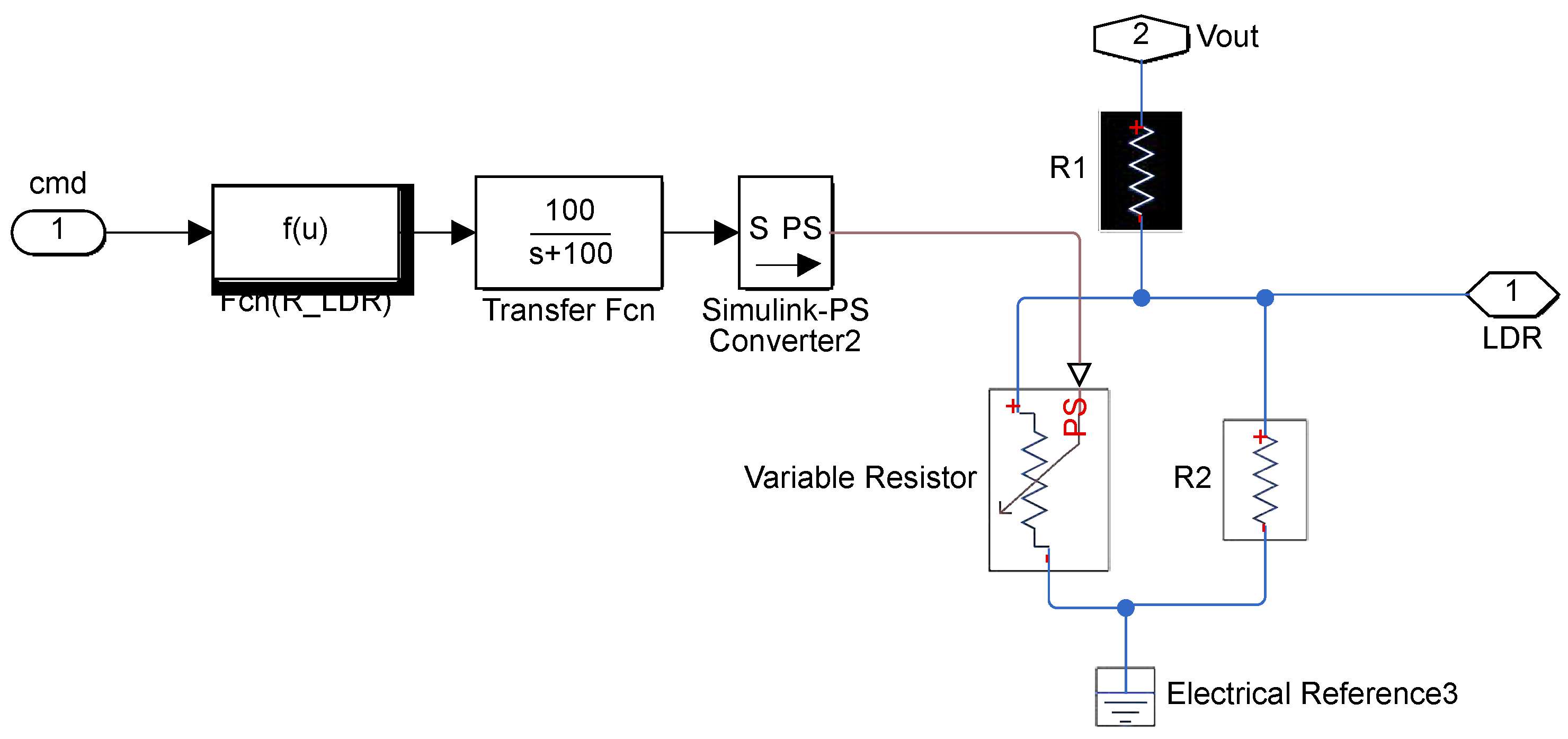
Figure 15 represents the circuit model of the LDR.
Figure 16 depicts the fuzzy controller for voltage regulation simulation. Current regulation simulation was carried out in a similar fashion. Results for the voltage regulation simulation are shown in
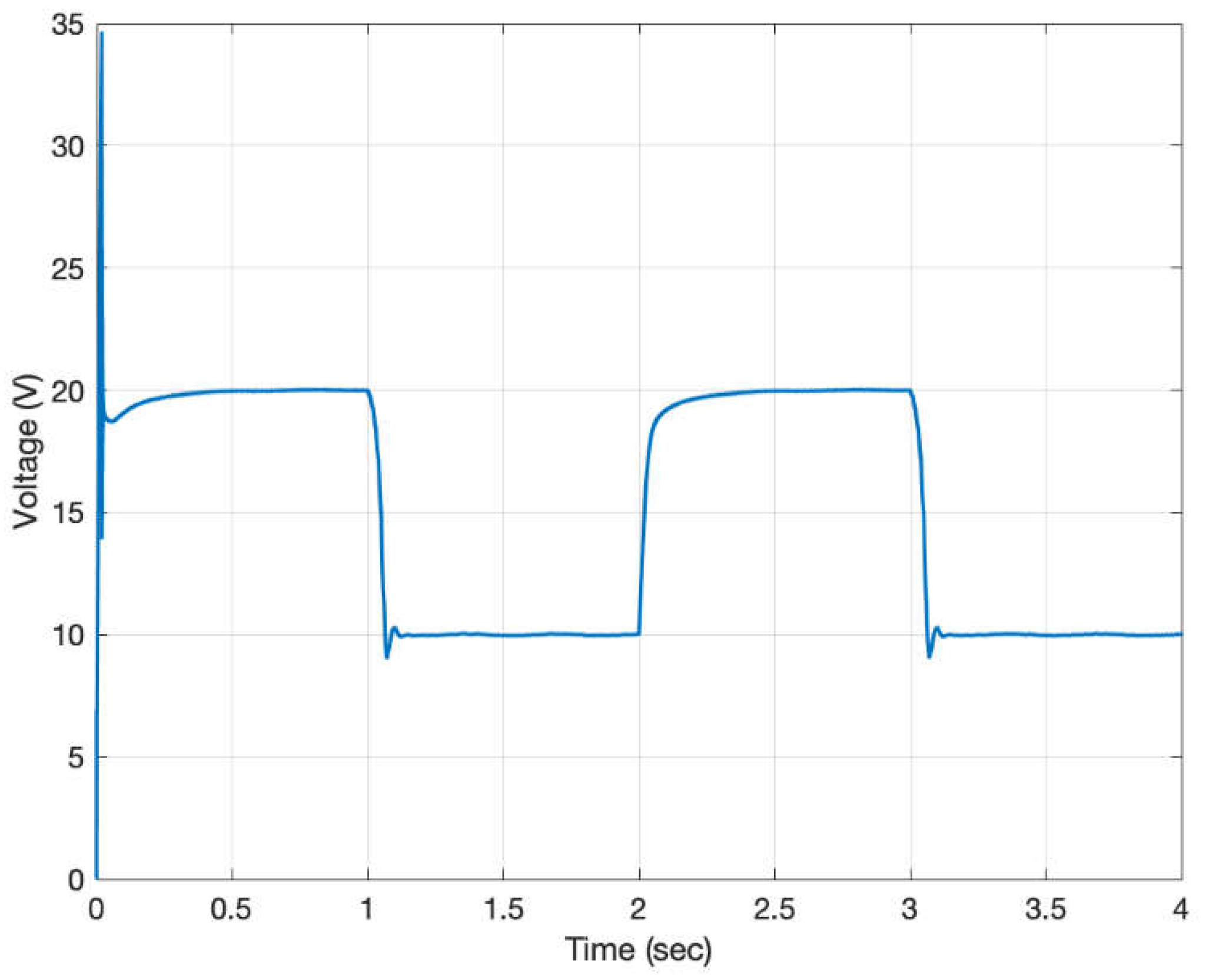
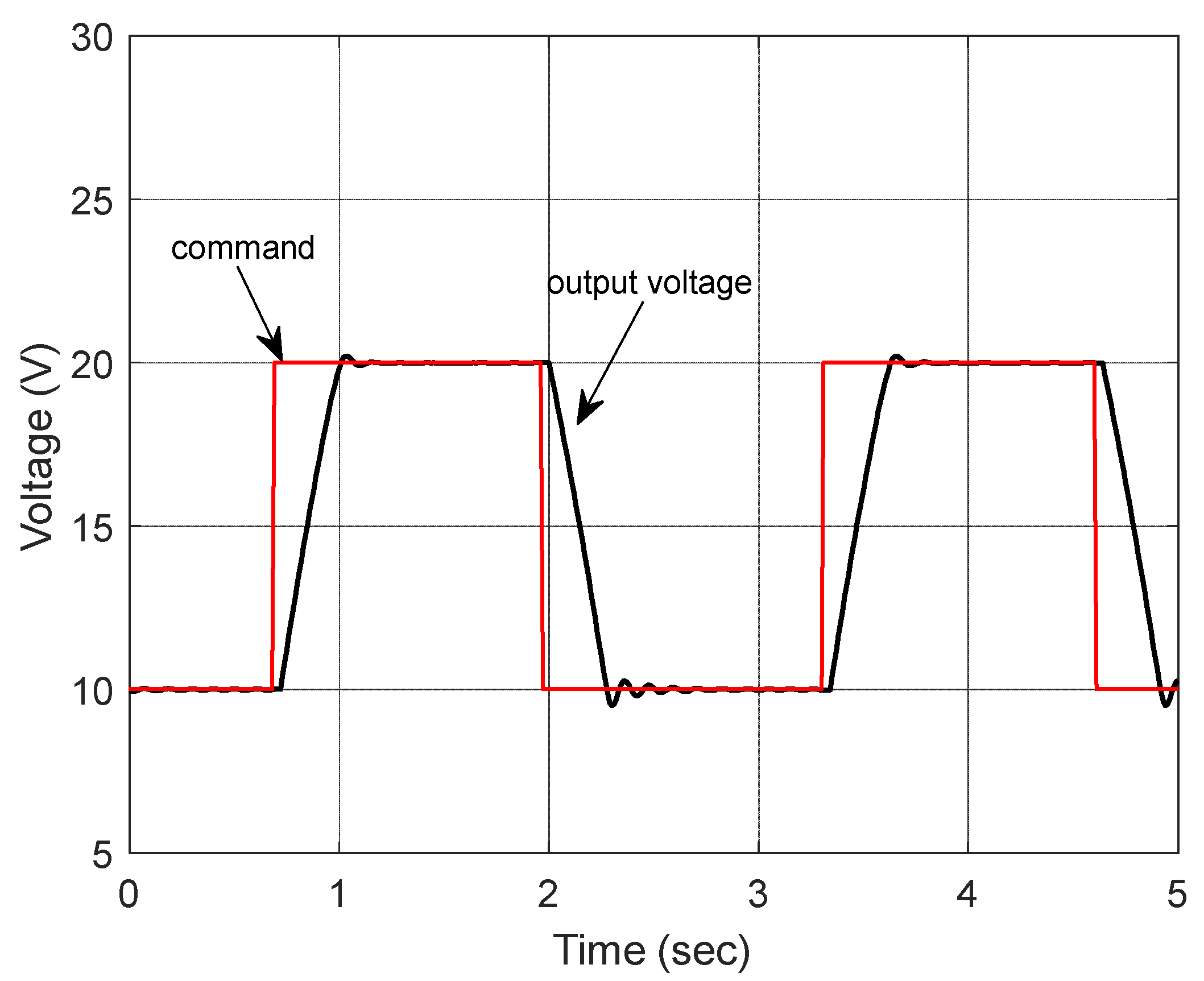
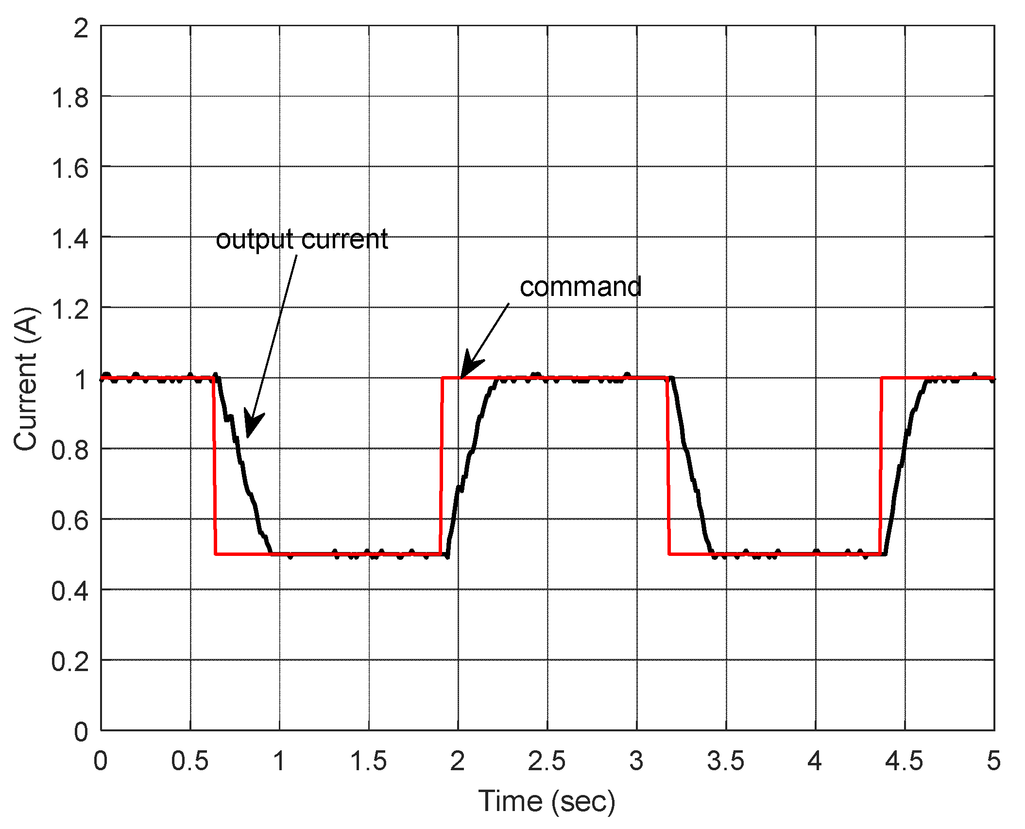
Figure 17. In the simulation the input voltage is 17 V, the output voltage is commanded to provide 20 V for the load for one second, then switched to 10 V for another second. The results clearly indicate the success of voltage regulation. Similarly, results for current regulation are given in
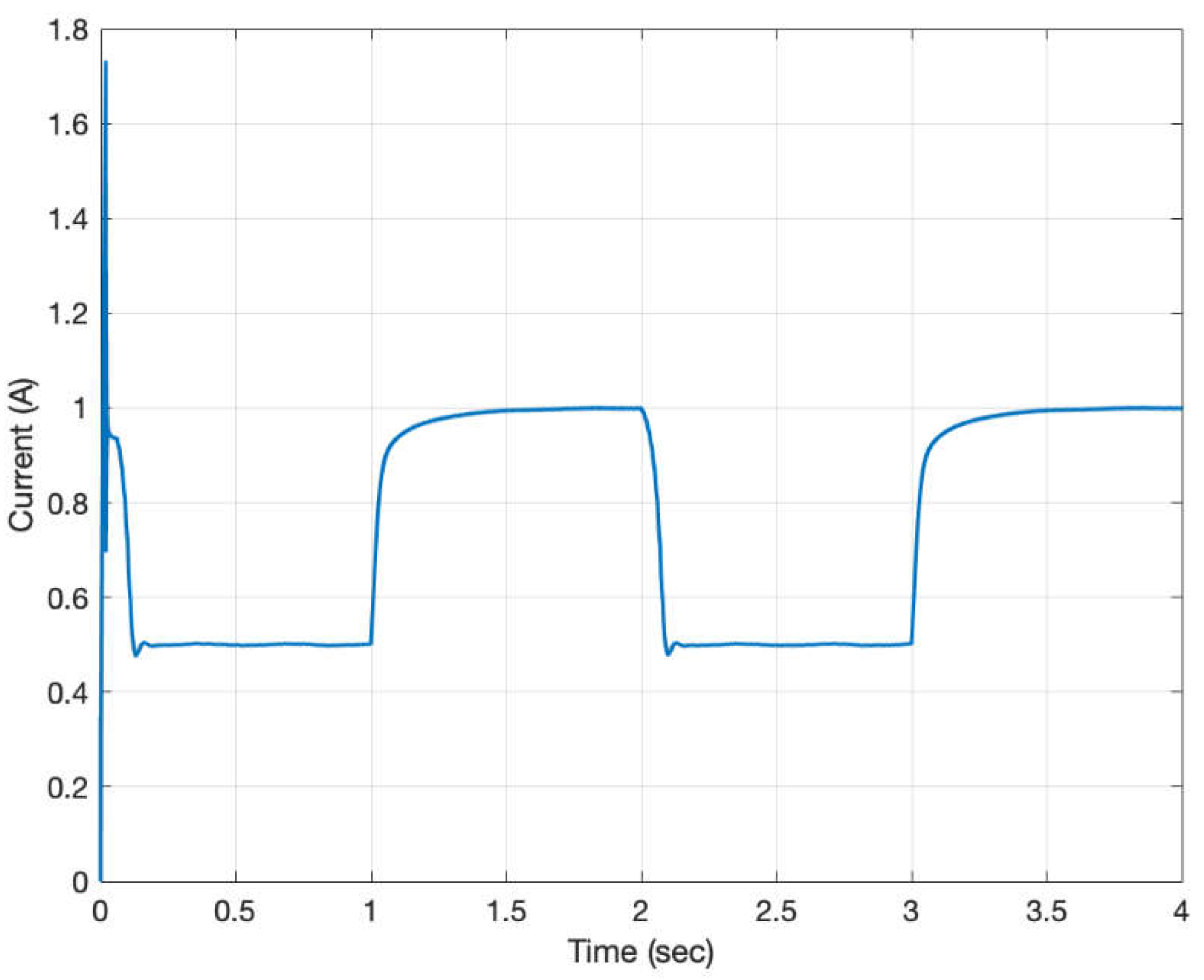
Figure 18. In the current regulation simulation, the output current is controlled to deliver 0.5 A to the load for one second, then switched to provide 1 A for another one second. Again, the results demonstrate the success of the design.


