Abstract
This paper presents an extremely cost-effective radio-frequency integrated circuit (RFIC) implementation technique by employing a digital logic CMOS process and reducing area occupation for voltage-controlled oscillators (VCOs) using all miniature inductors for wireless sensor network (WSN) applications. The designed VCO operates in the 4.0 GHz band with a power consumption of 1.4 mW and a phase noise of −113.6 dBc/Hz at 1 MHz, occupying a Si area of 0.283 × 0.682 mm2. In addition, we confirmed that the figure of merit (FOM) of 183.8 in our design is competitive with that of other LC-VCOs that were fabricated using the RF option and designed with conventional inductors.
1. Introduction
With the rapid proliferation of wireless applications, the demand for power and cost-effective radios has significantly increased [1]. A typical battery-powered wireless sensor node can last only for a few days. Thus, low power consumption is the critical factor to sustain long-term operation. In particular, wireless sensor networks (WSNs) are autonomous devices combining sensing, power, computation, and communication functions into a single system [2]. For this case, saving the unit cost is sometimes more important than extended lifetimes, combined with progress in CMOS and MEMS processing and a minimum number of off-chip components, since a typical sensor network consists of a large number of small, low-cost nodes that use wireless point-to-point communication to construct a self-organized network [3].
From this point of view, to save the cost of a radio-frequency integrated circuit (RFIC) for the WSN unit cell, our design approach was focused on ensuring circuit area minimization and adopting cost-effective CMOS processes, respectively. Miniature spiral inductors clearly have advantages for RFIC fabrication cost because they can consume less silicon area significantly. For example, 3D helical inductors (3HIs) occupy significantly less silicon area than planar spirals because the turn is expanded vertically [4]. For this reason, many miniature voltage-controlled oscillators (VCOs) using asymmetric-helical spirals embedded in core LC tanks or harmonic-rejection filters have been reported [4,5]. In this paper, we expand this concept to create and demonstrate a size-efficient VCO based on only miniature spirals. Moreover, to additionally save design costs of fabrication, our VCO was implemented using a CMOS process for pure digital and analog (1-poly and 6-metal) signals; no process changes were made to improve the high-frequency characteristics of the devices.
2. Extreme Cost-Effective LC-VCO Circuit Design
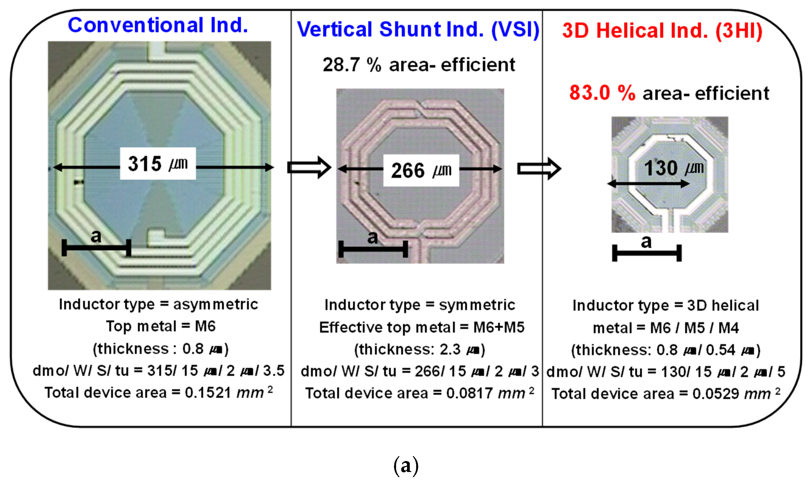
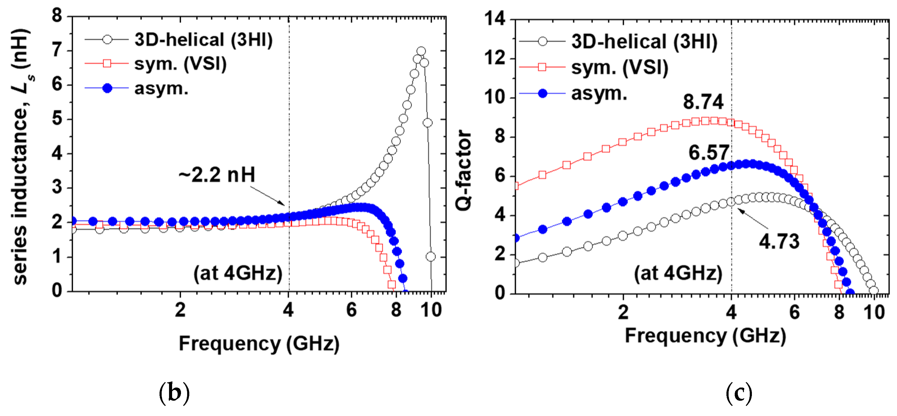
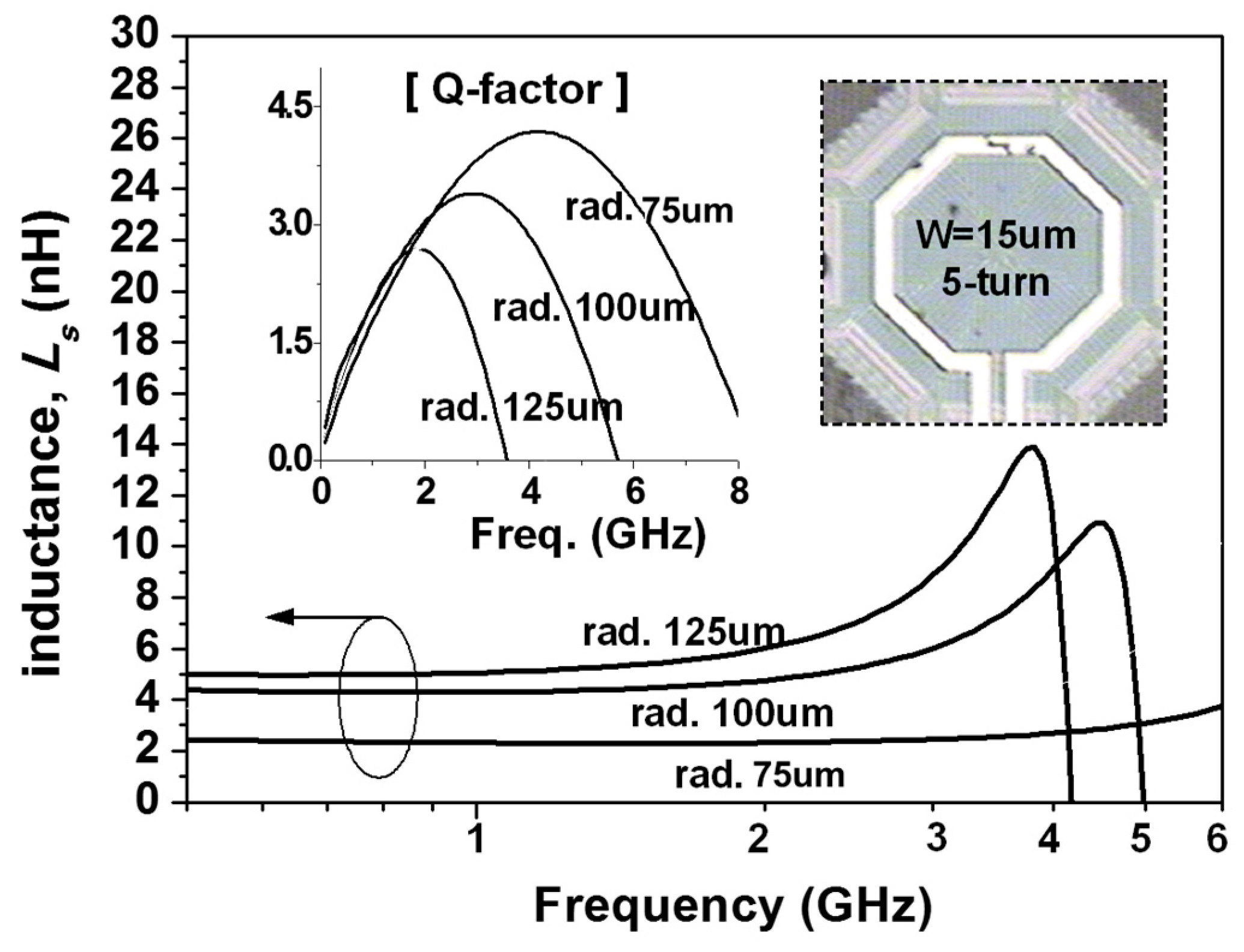
In LC-VCO design, inductor performance of the LC tank plays a critical role in the phase noise and output signal power, simultaneously. Thus, for a low-cost LC-VCO implemented using a low-cost digital logic CMOS process with a thin top metal thickness (<1.0 um), a vertical-shunt inductor (VSI) was a good candidate as a tank spiral in our design [4].The reason is that the VSI is implemented by the neighboring metal layers that are shunted through arrays, in a mixed-signal CMOS process, and the effective metal thickness of the spiral can be increased up to 2.3 μm, which is comparable to the top metal thickness of the RF CMOS process without any additional cost. Figure 1 shows that the VSI has a size reduction of 28.7% and a higher Q-factor (8.74) at 4 GHz from measurement results compared with the conventional one. In the case of the 3D inductor, such as a helical spiral, the turn is expanded vertically [5]. Thus, 3D helical inductors (3HIs) have the advantage of small area occupation compared with planar inductors. As shown in Figure 1, a size reduction of approximately 83% using 3HI compared with a conventional inductor was achieved in exchange for a Q-factor degradation of 20%, whereas the inductance value of 2.2 nH close to 4 GHz was almost same. It had only a 50 μm radius and a 5 turn ratio, vertically. Thus, when considering a low-cost design such as WSN applications, the use of 3HIs for LC-VCO becomes one of the attractive solutions for saving the Si area effectively, although the use of low-layer metals causes Q-factor degradation and reduces the current handling capability. Additionally, the series inductance (Ls) and Q-factor for 3HIs with radius variation were extracted from the measurement results and are shown in Figure 2:
where w, y21, and y11 represent angular frequency and y-parameters of a two-port network, respectively.
Ls = −Im (1/(w*y21)), Q-factor = −Im (y11)/Re(y11),
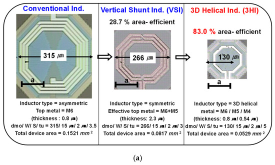
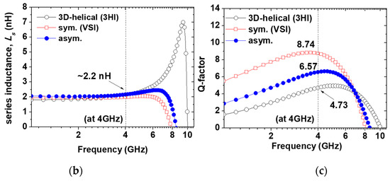
Figure 1.
(a) Representation of three different types (conventional, VSI, and 3HI) of inductors with same inductance of 2.2 nH. (b) Measured series inductance (Ls) and (c) their Q-factors at 4 GHz.
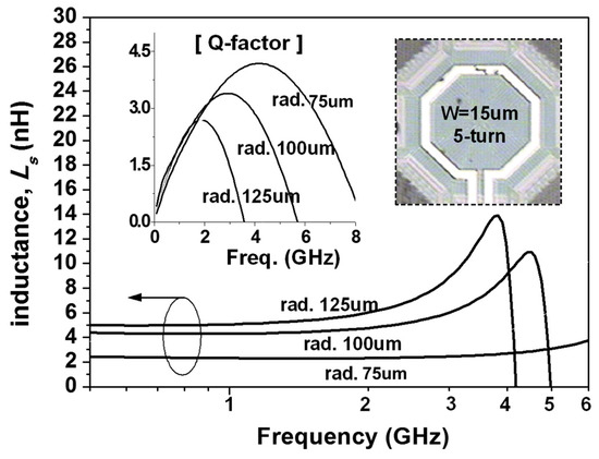
Figure 2.
Measured inductance (Ls) and Q-factors of fabricated symmetric helical inductors.
A schematic diagram of the designed VCO is shown in Figure 3a. To achieve a better phase-noise performance based on waveform symmetry and higher amplitude, two symmetric cross-coupled N/PMOS pairs (M1 to M4) were employed; their positive feedback effectively compensates for the LC tank loss caused by the 3HI, Ltank [5,6,7]. Additionally, another helical spiral was also used in the filtering technique. Lfilter, which is in series with the LC tank, encourages a high impedance supply voltage (Vdd) at 2 fo.
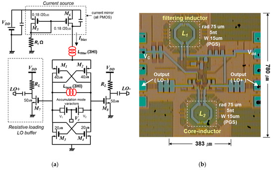
Figure 3.
(a) Designed LC-VCO schematic diagram. (b) Chip microphotograph (0.283 × 0.623 mm).
We used a large capacitor, Cx, to short noise frequencies around 2 fo. The LC tank consisted of one symmetric helical inductor and two MOS varactors (V1 and V2). A 2.2 nH differential inductor with a poly-shielded ground was used in the LC tank; it had a Q-factor of 4.2 at 4 GHz. The accumulation-mode MOS varactor with an n+ poly gate in the n-well was used for frequency tuning [8]. The measured capacitance varied from 230 fF to 290 fF and the varactor’s Q-factor was greater than 60. The effective parallel conductance of the LC tank was approximately 3.57 mS at 4.0 GHz. Thus, the required transconductance of NMOS (gmn) and PMOS (gmp) was 10.7 mS; in addition, the VCO bias current should be greater than 1 mA. However, for the definite oscillation and low phase noise within the current limited region, we had to increase the bias current flow in the VCO core; thus, the final DC current of the VCO was determined to be 1.3 mA.
3. Experimental Results
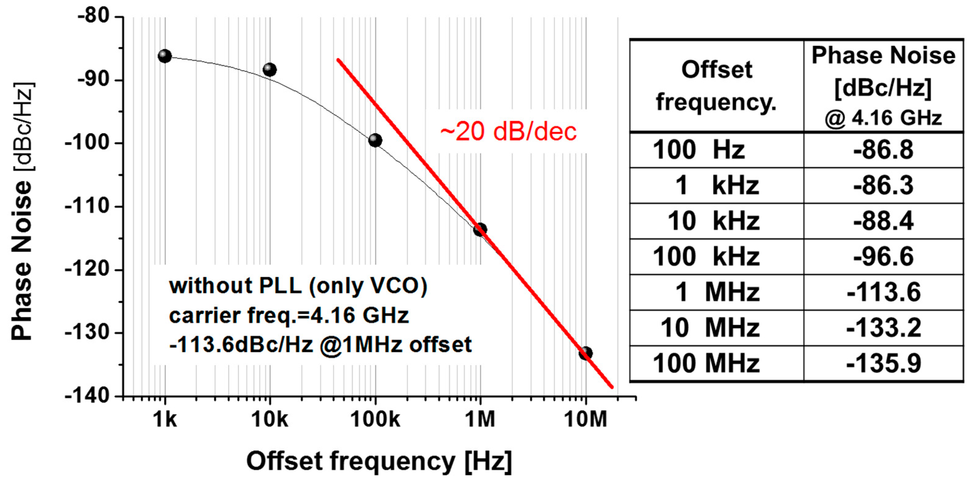
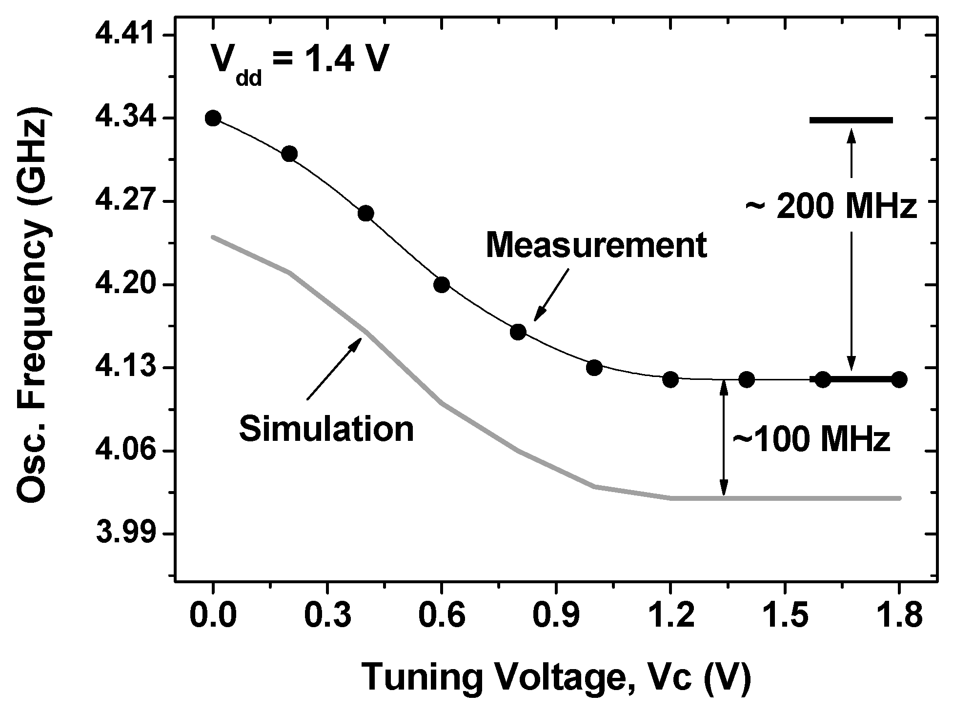
As shown in Figure 3b, the actual circuit area of the fabricated VCO (excluding pads) is 0.283 × 0.623 mm2. The all-helical-inductor-based VCO has the following key circuit parameters: transistor size M1 and M2 (W/L) = 40/0.18 μm, M3 and M4 (W/L) = 20/0.18 μm, radius of L1 and L2 = 50 μm, with values of 2.2 nH at 4 GHz. Moreover, to suppress substrate loss in the spiral, a poly-patterned ground shield (PGS) was added and grounded metal-1 shields were used underneath the MIM capacitors and RF interconnects [6]. Figure 4 shows the measurement results for phase noise performance with offset frequency. An output power greater than -13 dBm was achieved with 1.4 mW of DC power consumption. The oscillator operated from 4.13 GHz to 4.34 GHz as a function of the tuning voltage (Vc) and therefore had a tuning range of 4.8%. Additionally, the phase noise of the fabricated VCO was found to be −113.6 dBc/Hz at a 1 MHz offset. Figure 5 presents the simulated and measured tuning range that the performed simulation showed under the 3% model error. All measurement testing was performed using an on-wafer system using an Agilent 8565E spectrum analyzer (Santa Rosa, CA 95403-1799, USA), in terms of oscillation frequency, output power, and phase noise.
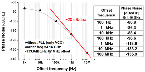
Figure 4.
Measured phase noise with offset frequency.

Figure 5.
Comparisons between measured and simulated results.
For the performance comparisons of different oscillators, the typical figure of merit (FOM) is used as defined by [9]:
where L (fm) represents the phase noise at an offset frequency from the carrier frequency fo.
Since a larger Si area is usually required to have a higher Q-factor of inductors, there is a trade-off between the Si occupation and FOM. Thus, the LC-VCO should be evaluated with another FOM (FoMA) that is normalized by area and described by the following equation [10]:
Table 1 summarizes the measurement results and compares them to those reported in [11,12,13,14,15,16] that were operated at the 3–5 GHz band. We show that our VCO has a comparable figure of merit and small silicon area occupation with cost-effective advantages.

Table 1.
Performance comparisons with reported VCOs.
4. Conclusions
A cost-effective LC-VCO fabricated using a 0.18 μm digital CMOS process composed of all miniature spirals was proposed. 3HIs have a size reduction of 85% compared with conventional spirals and were applied to the LC tank and harmonic filter of the miniature VCO. The implemented LC-VCO had a power consumption of 1.4 mW and a phase noise of −113.6 dBc/Hz at 1 MHz offset at a 4 GHz frequency band. This work shows that the use of a 3D spiral combined with mixed-signal CMOS technology allows for the low-cost RFIC realization for WSN applications.
Author Contributions
Methodology, validation, paper writing, conceptualization, H.J. investigation, M.-S.K. review, writing, C.-H.A. Funding acquisition, supervision, writing and editing, M.K.
Funding
This research was supported by the MOTIE (Ministry of Trade, Industry & Energy (10085645) and KSRC (Korea Semiconductor Research Consortium) support program for the development of the future semiconductor device. This research was also supported by Basic Science Research Program through the National Research Foundation of Korea (NRF) funded by the Ministry of Education (2018R1A6A1A03023788).
Conflicts of Interest
The authors declare no conflict of interest.
References
- Yao, Y.; Cao, Q.; Vasilakos, A.V. An energy-efficient, delay-aware, and lifetime-balancing data collection protocol for heterogeneous wireless sensor networks. IEEE/ACM Trans. Net. 2015, 23, 810–823. [Google Scholar] [CrossRef]
- Cattani, M.; Boano, C.A.; Römer, K. An Experimental Evaluation of the Reliability of LoRa Long-Range Low-Power Wireless Communication. J. Sens. Actuator Netw. 2017, 6, 7. [Google Scholar] [CrossRef]
- Viani, F.; Bertolli, M.; Salucci, M.; Polo, A. Low-Cost Wireless Monitoring and Decision Support for Water Saving in Agriculture. IEEE Sens. J. 2017, 17, 4299–4309. [Google Scholar] [CrossRef]
- Gil, J.; Song, S.-S.; Lee, H.; Shin, H. A −119.2 dBc/Hz at 1 MHz, 1.5 mW, fully integrated, 2.5-GHz, CMOS VCO using helical inductors. IEEE Microw. Wirel. Compon. Lett 2003, 13, 457–459. [Google Scholar]
- Lee, S.-H.; Chuang, Y.-H.; Chi, L.-R.; Jang, S.-L.; Lee, J.-F. A low-voltage 2.4GHz VCO with 3D helical inductors. IEEE APCCAS 2006, 518–521. [Google Scholar]
- Danesh, M.; Long, J.R. Differentially driven symmetric microstrip inductors. IEEE Trans. Microw Theory Tech. 2002, 50, 332–341. [Google Scholar] [CrossRef]
- Ooi, B.-L.; Xu, D.-X.; Kooi, P.-S. A comprehensive explanation on the high quality characteristics of symmetrical octagonal spiral inductor. Proc. IEEE Radio Freq. Integr. Circuits Symp. 2003, 259–262. [Google Scholar]
- Yue, C.P.; Wong, S.S. On-chip spiral inductors with patterned ground shields for Si-based RF IC’s. IEEE J. Solid-State Circuit 1998, 33, 743–752. [Google Scholar] [CrossRef]
- Hegazi, E.; Sjöland, H.; Abidi, A.A. A filtering technique to lower LC oscillator phase noise. IEEE J. Solid-State Circuits 2001, 36, 1921–1930. [Google Scholar] [CrossRef]
- Yu, S.-A.; Kinget, P.R. Scaling LC oscillators in nanometer CMOS technologies to a smaller area but with constant performance. IEEE Trans. Circuits Syst. II 2009, 56, 354–358. [Google Scholar]
- Moon, Y.-J.; Roh, Y.-S.; Jeong, C.-Y.; Yoo, C. A 4.39–5.26 GHz LC-Tank CMOS Voltage-Controlled Oscillator with Small VCO-Gain Variation. IEEE Microw. Wirel. Compon. Lett. 2009, 19, 524–526. [Google Scholar] [CrossRef]
- Park, D.; Cho, S.-H. H. A 1.8 V 900 μW 4.5 GHz VCO and Prescaler in 0.18 μm CMOS Using Charge-Recycling Technique. IEEE Microw. Wirel. Compon. Lett. 2009, 19, 104–106. [Google Scholar] [CrossRef]
- Lee, S.-H.; Chuang, Y.-H.; Jang, S.-L.; Chen, C.-C. Low-Phase Noise Hartley Differential CMOS Voltage Controlled Oscillator. IEEE Microw. Wirel. Compon. Lett. 2007, 17, 144–147. [Google Scholar] [CrossRef]
- Jerng, A.; Sodini, C.G. The impact of device type and sizing on phase noise mechanisms. IEEE J. Solid-State Circuits 2005, 40, 360–369. [Google Scholar] [CrossRef]
- Chu, Y.K.; Chuang, H.R. A fully integrated 5.8 GHz U-NII band 0.18-m CMOS VCO. IEEE Microw. Wirel. Compon. Lett. 2003, 13, 287–289. [Google Scholar]
- Tsai, M.-D.; Cho, Y.-H.; Wang, H. A 5-GHz low phase noise differential colpitts CMOS VCO. IEEE Microw. Wirel. Compon. Lett. 2005, 15, 327–329. [Google Scholar] [CrossRef]
© 2019 by the authors. Licensee MDPI, Basel, Switzerland. This article is an open access article distributed under the terms and conditions of the Creative Commons Attribution (CC BY) license (http://creativecommons.org/licenses/by/4.0/).

