Article

Effects of Equivalent-Oxide-Thickness and Fin-Width Scaling on In0.53Ga0.47As Tri-Gate Metal-Oxide-Semiconductor-Field-Effect-Transistors with Al2O3/HfO2 for Low-Power Logic Applications

School of Electrical Engineering, University of Ulsan, Ulsan 44610, Korea
Electronics 2020, 9(1), 29; https://doi.org/10.3390/electronics9010029
Submission received: 6 December 2019 / Revised: 24 December 2019 / Accepted: 24 December 2019 / Published: 26 December 2019
(This article belongs to the Section Microelectronics)

Abstract

:
We created tri-gate sub-100 nm In0.53Ga0.47As metal-oxide-semiconductor-field-effect-transistors (MOSFETs) with a bi-layer Al2O3/HfO2 gate stack and investigated the scaling effects on equivalent-oxide-thickness (EOT) and fin-width (Wfin) at gate lengths of sub-100 nm. For Lg = 60 nm In0.53Ga0.47As tri-gate MOSFETs, EOT and Wfin scaling were effective for improving electrostatic immunities such as subthreshold swing and drain-induced-barrier-lowering. Reliability characterization for In0.53Ga0.47As Tri-Gate MOSFETs using constant-voltage-stress (CVS) at 300K demonstrates slightly worse VT degradation compared to planar InGaAs MOSFET with the same gate stack and EOT. This is due to the effects of both of the etched fin’s sidewall interfaces.

1. Introduction

Traditional SiO2/Si-based gate stack downscaling has approached its fundamental and applied limits due to high current density leakage through ultrathin SiO2 and the material limitations of Si. This impacts the Metal-Oxide-Semiconductor Field-Effect-Transistor (MOSFET) operating speed, reliability, condensed device density, and power consumption. Indium-rich InxGa1−xAs channel materials, where x > 0.53, are the most promising non-Si n-channel candidates for next-generation Complementary-MOS (CMOS) technology at and beyond the 5-nm technology node. The most promising new technology is a combination of a high-k oxide and III-V channel materials because of outstanding carrier transport properties such as the effective electron mobility (µn) and injection velocity (νx0) [1,2,3,4,5,6]. For the past three decades, a key bottleneck in developing III-V MOSFETs has been poor interface state quality between the oxide and III-V channel [7,8,9,10,11]. Atomic-layer-deposition (ALD) provides a very good quality interface, presumably due to the “self-cleaning effect” during the high-k deposition, especially in the In0.53Ga0.47As channel [12,13,14,15]. The high-k gate dielectric can reduce leakage current through a thick physical dimension while keeping an equivalent oxide thickness (EOT). Recently, using the ALD process, our group demonstrated a tri-gate In0.53Ga0.47As MOSFET and an ultra-thin-body (UTB) planar InGaAs MOSFET with high-k gate stacks. This indicated an excellent interface trap density (Dit) [16]. Among the high-k dielectrics Al2O3, HfO2, La2O3, ZrO2 and TiO2 oxides that have been studied, no single dielectric is a clear leading contender. However, both Al2O3 and HfO2 are quite attractive due to the ease of fabrication using the ALD process. Even though Al2O3 has a comparatively large bandgap (~8.8 eV), a good interfacial boundary with a self-cleaning effect, high thermal stability, fewer active electrical defects and a moderate dielectric constant (k = 6–9). Conversely, even though HfO2 has a higher dielectric constant (k = 20–25) and moderate bandgap (~5.7 eV), it has lower thermal and interfacial stabilities, larger hysteresis, a higher leakage tendency, and more active electrical traps. Using this information, we created an InGaAs MOSFET with Al2O3/HfO2 bi-layer gate stack scaled down to an EOT below 1 nm [16,17]. The UTB planar InGaAs MOSFET with Al2O3/HfO2 exhibits outstanding performance parameters, including S = 69 mV/dec, DIBL < 10 mV/V, C-V hysteresis < 10 mV/V with Dit = 2.7 × 10¹² /cm2-eV and EOT ≈ 0.7 nm [16,17].
For a deeply scaled-down transistor using 5-nm technology, body thickness (tbody) has to be thinned down in such a way that Lg can maintain electrostatic immunity. However, thinning down tbody degrades the carrier transport and increases parasitic resistance in the channel. A non-planar structure with a tri-gate configuration is an effective way to improve electrostatic immunity while preserving the carrier transport’s ability to maintain parasitic resistance [18,19].
In this paper, we address the benefits of EOT and fin-width scaling on subthreshold swing and DIBL in tri-gate InGaAs MOSFETs. We also demonstrate preliminary reliability characterization to verify the etched fin’s sidewall interface and damages when the devices are in operation mode.

2. Materials and Methods

The device fabrication process started with a conventional sequence of mesa isolation with H3PO4-based wet chemistry to isolate the current path. Non-alloyed Mo-based ohmic contact for S/D was evaporated on top of a heavily doped InGaAs cap layer. This was followed by two E-beam lithography steps consisting of fin formation for non-planar structures. Next, the gate was recessed to expose an area for the high-k gate stack. This was done utilizing wet-based chemistry. Two types of high-k, Al2O3/HfO2 (0.7 nm/1.6 nm) and Al2O3 (3 nm), were deposited to split the EOT. Their corresponding EOTs were ≈ 0.7 nm for Al2O3/HfO2 (0.7 nm/1.6 nm) and ≈ 2 nm for Al2O3 (3 nm). ALD-based 20-nm TiN was deposited for the metal-gate (MG). The process flow was conducted below 350 °C to avoid any thermal damage to the gate region. The completed tri-gate InGaAs MOSFET had an Lg = 60 nm, 20 nm fin-height (Hfin), and fin-width (Wfin) range from 60 nm to 30 nm. The effective gate-width (Wg_eff) was calculated using the equation Wfin + 2 × Hfin. A planar type InGaAs MOSFET was also made with an ultra-thin-body (5 nm) and Al2O3/HfO2 (0.7 nm/1.6 nm) gate stack. Figure 1 shows the conceptual architecture of the 3D tri-gate In0.53Ga0.47As MOSFET and a cross-sectional schematic of each fin along the gate-length direction. We also made a MOS capacitor on top of the InGaAs surface to optimize the interface trap.
Figure 2 shows the corresponding C–VGS measurement at VDS = 0 V for a planar MOSFET with Al2O3 (left) and Al2O3/HfO2 (right) from 10 kHz to 1 MHz. Both C–VGS curves exhibit small frequency dispersion in a strong accumulation region. The hump near the off-state is a consequence of Dit. Inset is the C–VG from MOSCAPs with the same gate stacks, where EOT is extracted to 2 nm for the Al2O3 gate stack and 0.7 nm for the Al2O3/HfO2 gate stack. For the planar MOSFET with the Al2O3/HfO2 gate stack, the gate capacitance is 15.5 fF/μm2 at VGS–VT = 0.5 V, the highest for any MOSFETs.
From C–VGS and ID–VGS at the linear bias regime (VDS = 0.05 V) for planar MOSFETs, effective mobility (μeff) can be determined. Even with an EOT of sub-1nm, the planar InGaAs MOSFET yields a μeff in excess of 3000 cm2/V-s at 300 K. This is 5 times higher than Si universal mobility reported in the literature [20].

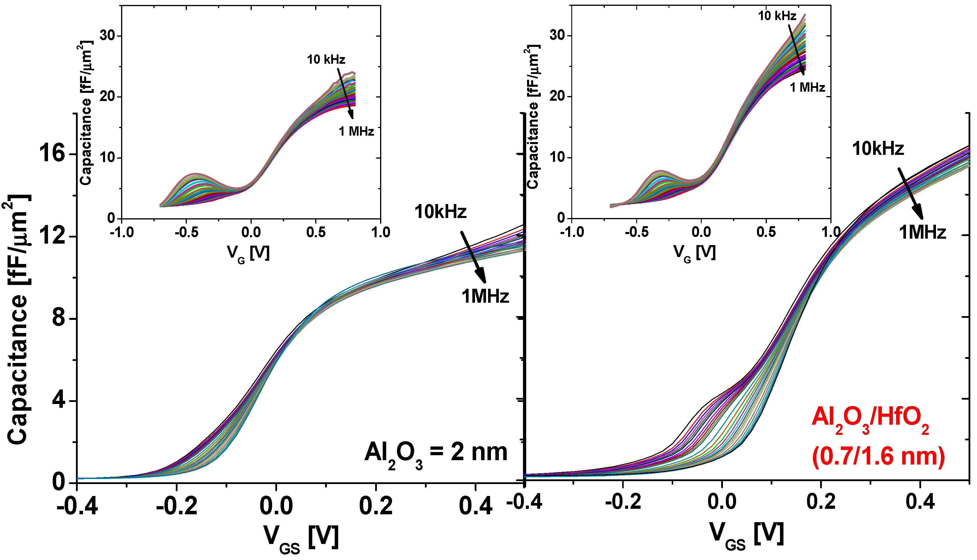
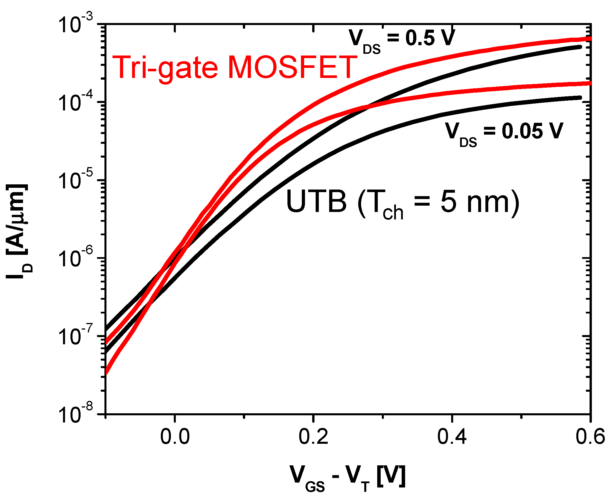
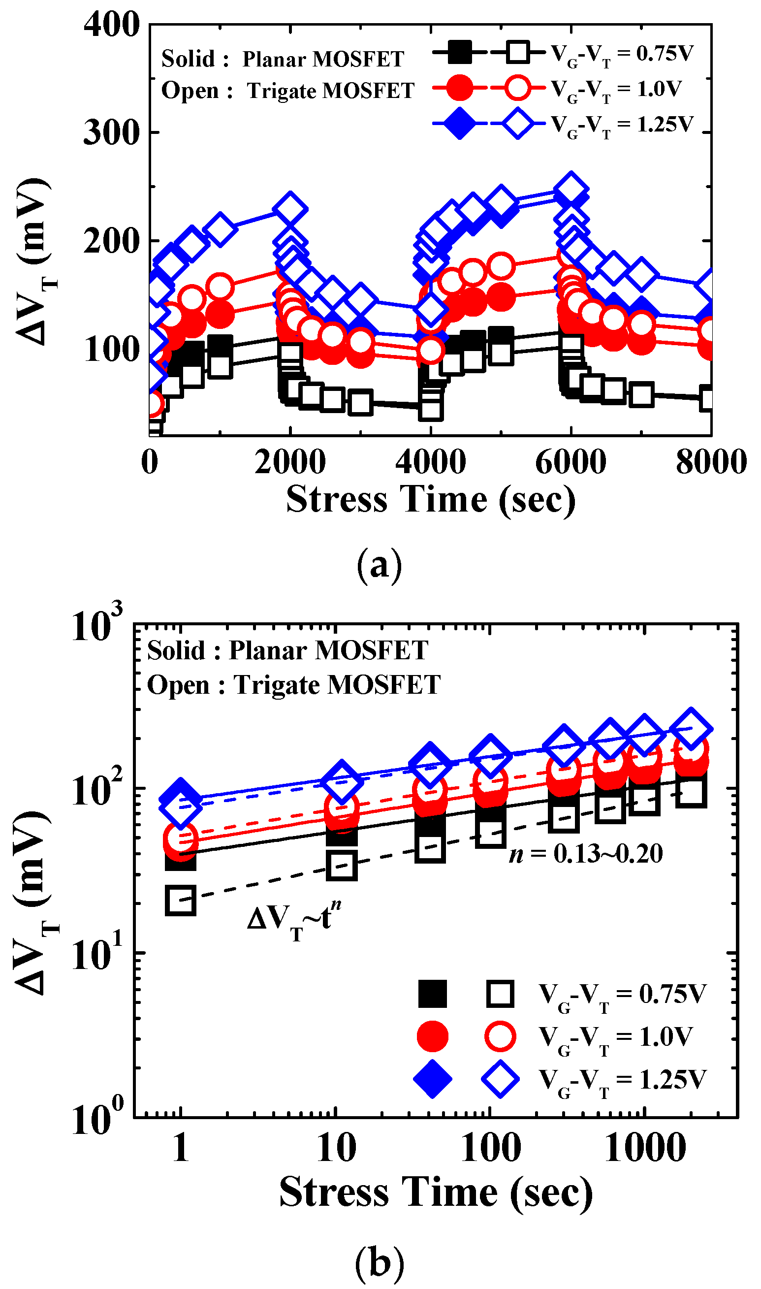
3. Results and Discussion

Figure 3 shows the subthreshold characteristics of Lg = 60 nm tri-gate InGaAs MOSFET with different values of EOT and Wfin. Figure 3a depicts EOT scaling from 2 nm to 0.7 nm with Wfin = 60 nm. EOT = 0.7 nm, with S = 94 mV/dec. and DIBL = 40 mV/V, is better than EOT = 2 nm, where S = 104 mV/dec. and DIBL = 54 mV/V. Figure 3b depicts Wfin scaling from 60 nm to 30 nm with EOT = 0.7 nm. This highlights how Wfin scaling improves the electrostatic integrity in tri-gate InGaAs MOSFET devices. When EOT = 0.7 nm, the device with Wfin = 30 nm shows an improvement of S and DIBL (S = 77 mV/dec. and DIBL = 10 mV/V) compared to Wfin = 60 nm (S = 94 mV/dec. and DIBL = 40 mV/V). The inset shows S as a function of Vgs.
Figure 4 shows a comparison between the subthreshold characteristics of the tri-gate MOSFET with Lg = 60 nm, Wfin = 30 nm and the ultra-thin-body (UTB) planar MOSFET with Lg = 50 nm. The UTB planar MOSFET was reported previously and has a similar physical gate length [21]. The tri-gate InGaAs MOSFET shows a much sharper subthreshold swing and less DIBL at the measured regime. This means the tri-gate MOSFET provides better electrostatics and higher values of ON-current (ION) than the planar MOSFET with a similar physical gate length.
To investigate the plasma-etched sidewall fin surfaces, we conducted a reliability characterization of the planar InGaAs MOSFET and non-planar tri-gate InGaAs MOSFET using constant-voltage-stress (CVS) at 300 K. Figure 5 shows that VT shifts as a function of stress time under CVS iterations and relaxes at 300 K for the tri-gate and planar MOSFETs. The tri-gate MOSFET shows slightly more VT degradation than the planar MOSFET. At 2000 s of stress time, the tri-gate MOSFET shows a shift in ΔVT of 90 mV at VG–VT = 1.25 V, presumably due to the effect of the sidewall interface from the etched fin. Further surface cleaning processes such as high-pressure annealing (HPA) will help improve the etched surface after the fin etching process.

4. Conclusions

We investigated the effect of EOT and Wfin on the electrostatic integrity of tri-gate InGaAs MOSFETs at gate lengths in the sub-100 nm regime. EOT and Wfin scaling help to improve the short-channel effects. In addition, reliability characterization for InGaAs tri-Gate MOSFETs using constant-voltage-stress (CVS) at 300 K revealed slightly more VT degradation compared to planar InGaAs MOSFETs with the same gate stack and EOT. This indicates that the etched fin effect on both sidewall interfaces is not a concern for the etched tri-gate process.

Author Contributions

T.-W.K. conducted most of the experiments, wrote the manuscript, initiated the work, and supervised the process. Author has read and agreed to the published version of the manuscript.

Funding

This research was supported by Civil-Military Technology Cooperation Program (No. 19-CM-BD-05).

Conflicts of Interest

The authors declare no conflict of interest.

References

  1. Del Alamo, J.A. Nanometre-scale electronics with III–V compound semiconductors. Nature 2011, 479, 317–323. [Google Scholar] [CrossRef] [PubMed]
  2. Lin, H.C.; Wang, W.E.; Brammertz, G.; Meuris, M.; Heyns, M. Electrical study of sulfur passivated In0.53Ga0.47As MOS capacitor and transistor with ALD Al2O3 as gate insulator. Microelectron. Eng. 2009, 86, 1554–1557. [Google Scholar] [CrossRef]
  3. Lin, D.; Brammertz, G.; Sioncke, S.; Fleischmann, C.; Delabie, A.; Martens, K.; Bender, H.; Conard, T.; Tseng, W.H.; Lin, J.C.; et al. Enabling the high-performance InGaAs/Ge CMOS: A common gate stack solution. In Proceedings of the 2009 IEEE International Electron Devices Meeting (IEDM), Baltimore, MD, USA, 7–9 December 2009; IEEE: Piscataway, NJ, USA, 2009; pp. 1–4. [Google Scholar]
  4. Heyns, M.; Alian, A.; Brammertz, G.; Caymax, M.; Chang, Y.C.; Chu, L.K.; De Jaeger, B.; Eneman, G.; Gencarelli, F.; Groeseneken, G.; et al. Advancing CMOS beyond the Si roadmap with Ge and III/V devices. In Proceedings of the 2011 International Electron Devices Meeting, Washington, DC, USA, 5–7 December 2011; IEEE: Piscataway, NJ, USA, 2011; Volume 3, pp. 13.1.1–13.1.4. [Google Scholar]
  5. Takagi, S.; Iisawa, T.; Tezuka, T.; Numata, T.; Nakaharai, S.; Hirashita, N.; Moriyama, Y.; Usuda, K.; Toyoda, E.; Dissanayake, S.; et al. Carrier-Transport-Enhanced Channel CMOS for Improved Power Consumption and Performance. IEEE Trans. Electron Devices 2008, 55, 21–39. [Google Scholar] [CrossRef]
  6. Son, S.-W.; Park, J.-H.; Baek, J.-M.; Kim, J.S.; Kim, D.-K.; Shin, S.H.; Banerjee, S.K.; Lee, J.-H.; Kim, T.-W.; Kim, D.-H. Performance and carrier transport analysis of In0.7 Ga0.3 As quantum-well MOSFETs with Al2O3 /HfO2 gate stack. Solid State Electron. 2016, 123, 63–67. [Google Scholar] [CrossRef]
  7. Chidambaram, T.; Veksler, D.; Madisetti, S.; Yakimov, M.; Tokranov, V.; Oktyabrsky, S. InGaAs Inversion Layer Mobility and Interface Trap Density From Gated Hall Measurements. IEEE Electron Device Lett. 2016, 37, 1547–1550. [Google Scholar] [CrossRef]
  8. Netsu, S.; Hellenbrand, M.; Zota, C.B.; Miyamoto, Y.; Lind, E. A Method for Determining Trap Distributions of Specific Channel Surfaces in InGaAs Tri-Gate MOSFETs. IEEE J. Electron Devices Soc. 2018, 6, 408–412. [Google Scholar] [CrossRef]
  9. Engel-Herbert, R.; Hwang, Y.; Stemmer, S. Quantification of trap densities at dielectric/III–V semiconductor interfaces. Appl. Phys. Lett. 2010, 97, 062905. [Google Scholar] [CrossRef] [Green Version]
  10. Engel-Herbert, R.; Hwang, Y.; Chobpattana, V.; Stemmer, S. Correct determination of trap densities at high-k/III-V interfaces. In Proceedings of the CS MANTECH Conference, New Orleans, LA, USA, 13–16 May 2013; pp. 185–188. [Google Scholar]
  11. Veksler, D.; Bersuker, G.; Morassi, L.; Yum, J.H.; Verzellesi, G.; Wang, W.; Kirsch, P.D. Extraction of interfacial state density in high-k/III-V gate stacks: Problems and solutions. In Proceedings of the IEEE Nano Materials and Device Conference, Beijing, China, 5–8 August 2013; pp. 1–2. [Google Scholar]
  12. Chang, C.-H.; Chiou, Y.-K.; Chang, Y.-C.; Lee, K.-Y.; Lin, T.-D.; Wu, T.-B.; Hong, M.; Kwo, J. Interfacial self-cleaning in atomic layer deposition of HfO2 gate dielectric on In0.15Ga0.85As. Appl. Phys. Lett. 2006, 89, 242911. [Google Scholar] [CrossRef]
  13. Jevasuwan, W.; Urabe, Y.; Maeda, T.; Miyata, N.; Yasuda, T.; Yamada, H.; Hata, M.; Taoka, N.; Takenaka, M.; Takagi, S. Initial Processes of Atomic Layer Deposition of Al2O3 on InGaAs: Interface Formation Mechanisms and Impact on Metal-Insulator-Semiconductor Device Performance. Materials 2012, 5, 404–414. [Google Scholar] [CrossRef] [PubMed] [Green Version]
  14. Timm, R.; Head, A.R.; Yngman, S.; Knutsson, J.V.; Hjort, M.; McKibbin, S.R.; Troian, A.; Persson, O.; Urpelainen, S.; Knudsen, J.; et al. Self-cleaning and surface chemical reactions during hafnium dioxide atomic layer deposition on indium arsenide. Nat. Commun. 2018, 9, 1412. [Google Scholar] [CrossRef] [PubMed] [Green Version]
  15. Hinkle, C.L.; Sonnet, A.M.; Vogel, E.M.; McDonnell, S.; Hughes, G.J.; Milojevic, M.; Lee, B.; Aguirre-Tostado, F.S.; Choi, K.J.; Kim, H.C.; et al. GaAs interfacial self-cleaning by atomic layer deposition. Appl. Phys. Lett. 2008, 92, 071901. [Google Scholar] [CrossRef] [Green Version]
  16. Kim, T.-W.; Koh, D.; Kwon, H.; Shin, C.-S.; Park, W.-K.; Shin, S.H.; Cho, Y.; Ko, D.-H.; Hill, R.J.W.; Maszara, W.P.; et al. In0.7 Ga0.3 As quantum well MOSFETs with Al2O3/HfO2 toward subthreshold swing of ∼60 mV/dec. Appl. Phys. Express 2014, 7, 074201. [Google Scholar] [CrossRef]
  17. Kim, T.-W.; Koh, D.-H.; Shin, C.-S.; Park, W.-K.; Orzali, T.; Hobbs, C.; Maszara, W.P.; Kim, D.-H. Lg = 80-nm Trigate Quantum-Well In0.53 Ga0.47 as Metal–Oxide–Semiconductor Field-Effect Transistors With Al2O3/HfO2 Gate-Stack. IEEE Electron Device Lett. 2015, 36, 223–225. [Google Scholar] [CrossRef]
  18. Crupi, G.; Schreurs, D.M.M.; Rakin, J.P.; Caddemi, A. A comprehensive review on microwave FinFET modeling for progressing beyond the state of art. Solid State Electron. 2013, 80, 81–95. [Google Scholar] [CrossRef]
  19. Crupi, G.; Schreurs, D.M.M.; Rakin, J.P.; Caddemi, A. Effects of Gate-Length Scaling on Microwave MOSFET Performance. Electronics 2017, 6, 62. [Google Scholar] [CrossRef] [Green Version]
  20. Takagi, S.I.; Toriumi, A.; Iwase, M.; Tango, H. On the universality of inversion layer mobility in Si MOSFETs: Part I—Effects of substrate impurity concentration. IEEE Trans. Electron Devices 1994, 41, 2357–2362. [Google Scholar] [CrossRef]
  21. Kim, T.-W.; Kim, D.-H.; Koh, D.-H.; Hill, R.J.W.; Lee, R.T.P.; Wong, M.H.; Cunningham, T.; del Alamo, J.A.; Banerjee, S.K.; Oktyabrsky, S.; et al. ETB-QW InAs MOSFET with scaled body for improved electrostatics. In Proceedings of the 2012 International Electron Devices Meeting, San Francisco, CA, USA, 10–13 December 2012; IEEE: Piscataway, NJ, USA, 2012; pp. 32.3.1–32.3.4. [Google Scholar]
Figure 1. (a) Tri-gate InGaAs Quantum-Well (QW) MOSFET architecture. Bi-layer high-k (HK) gate dielectric stacks with Al2O3/HfO2 were used, followed by ALD-based TiN deposition. Fin geometry is 20 nm fin-height (Hfin) and fin-width (Wfin) ranging from 60 nm to 30 nm. (b) Cross-sectional schematics of each fin along the gate-length direction are shown in (b). This is equivalent to SOI Tri-gate MOSFET architecture.
Electronics 09 00029 g001
Figure 2. C–VGS measurement at VDS = 0 V for planar MOSFETs with Al2O3 (left) and Al2O3/HfO2 (right) from 10 kHz to 1 MHz. Inset is C–VG from MOSCAP with same gate stacks. Both C–VGS curves show small frequency dispersion in strong accumulation regions, the hump near off-state is a consequence of Dit. For devices with Al2O3/HfO2 gate stacks, Cg is 15.5 fF/μm2 (VGS–VT =0.5 V), the highest in any of the MOSFETs.
Electronics 09 00029 g002
Figure 3. Subthreshold characteristics comparison of Lg = 60 nm tri-gate InGaAs MOSFET depending on Wfin and EOT scaling. (a) EOT scaling at Wfin = 60 nm and (b) Wfin scaling at EOT = 0.7 nm.
Electronics 09 00029 g003
Figure 4. Benchmarks of subthreshold characteristics for both Lg = 60 nm tri-gate InGaAs MOSFET and Lg = 50 nm UTB planar MOSFET.
Electronics 09 00029 g004
Figure 5. VT shift as a function of stress time under iterations of (a) CVS (Constant-Voltage-Stress) and (b) relaxation at 300K for tri-gate and planar MOSFETs.
Electronics 09 00029 g005

