Article

A Novel Metal Foreign Object Detection for Wireless High-Power Transfer Using a Two-Layer Balanced Coil Array with a Serial-Resonance Maxwell Bridge

1
Department of System Semiconductor Engineering, Sangmyung University, Cheonan-si 31066, Korea
2
Korea Electronics Technology Institute, Seoul 03924, Korea
3
EMF Safety Inc., Yongin-si, Gyeonggi-do 16890, Korea
*
Author to whom correspondence should be addressed.
Electronics 2020, 9(12), 2070; https://doi.org/10.3390/electronics9122070
Submission received: 31 October 2020 / Revised: 28 November 2020 / Accepted: 1 December 2020 / Published: 4 December 2020
(This article belongs to the Special Issue Wireless Power/Data Transfer, Energy Harvesting System Design)

Abstract

:
In a wireless high-power transfer system with a distance of several tens of centimeters apart between the transmitter and receiver coils, one of the most challenging issues is to detect metallic foreign objects between the transmitter and receiver coils. The metallic foreign objects must be detected and removed since these reduce the transmission efficiency and cause heat generation of the transmitter and receiver. This paper presents two-layer symmetric balanced coil array so that if there are metallic foreign objects, it can be detected through the change of the inductance of the balanced coils. Since the balanced coil is composed of coils that are in a symmetrical relationship in position, there is no need for a reference coil, and interference between coils is reduced by dividing the coil into two layers. In addition, a novel serial-resonance Maxwell bridge circuit to improve the inductance change detection performance is presented in this paper. The proposed metallic foreign object detection system is implemented using two-layer balanced coil array with a serial-resonance Maxwell bridge and the experimental results show that voltage changes of hundreds of mV to several V occur when a metallic foreign object is inserted, so that even small metals such as clips can be detected.

1. Introduction

Recently, research on wireless power transfer (WPT) has been focused on wireless charging of large mobile devices such as electric vehicles, automatic guided vehicles, and robots beyond wireless small devices such as mobile phones, smart watches and wearable devices [1,2,3]. Since it requires thousands of times more power than conventional small devices, high-power WPT has additional requirements for safety during charging as well as the requirements for charging efficiency [4,5]. Therefore, technologies such as unwanted emission electromagnetic field reduction, heat control, foreign object detection (FOD), position detection (PD), and human safety have attracted more attention [6,7]. In particular, technology that detects metallic foreign objects (MO) such as coins, keys, and foil not only reduces transmission efficiency, but can also cause circuit damage or fire, and even life-threatening if creatures such as cats and dogs get in between. Therefore, technologies such as FOD including metal object detection (MOD) and live object detection (LOD) are defined as very important technologies in the application of the product and are also defined as essential elements that must be observed in industry standardization organizations such as the Wireless Power Consortium (WPC) and Society of Automotive Engineers (SAE) International.
The Qi Wireless Power Transfer System Power Class 0 Specification version 1.2.3 proposes two FOD methods [8]. The first method monitors the temperature change at the interface surface of the transmitter. Another method monitors power loss between the transmitting interface and the receiving interface. However, in the case of high-power WPT, it is not appropriate to apply the methods proposed by Qi WPT. This is because the power loss caused by a metallic foreign object (MO) is very small compared to the output power in high-power WPT systems, making it difficult to detect. In addition, if there is a separation distance between the transmitter coil and receiver coil unlike the low-power WPC system, the distance between the coils is not constant and the power transfer efficiency varies greatly by misalignment [9,10]. Although SAE International’s J2954 wireless power transfer for light-duty plug-in/electrical vehicles and alignment methodology does not propose specific FOD methods, it is regulated to conduct MOD test including coins, paper clips, steel sheet, beverage cans, etc. [6,11].
For FOD methods in high-power WPT, wave-based detection methods and field-based detection methods are considered [6]. Wave-based detection methods require additional sensing devices such as imaging cameras, thermal cameras, or radar sensors to detect the presence of foreign objects. Thus the method has a high cost and is difficult to integrate with the power transfer system. The field-based detection method is a method of detecting a change in a magnetic field generated by the metal objects. To this end, a detection coil other than the transmitter coil and the receiver coil is added, and placed between the transmitter coil and the receiver coil to detect change in the characteristics of the detection coil. However, since the characteristics of the detection coil are also affected by the location of the receiver coil and the surrounding conditions such as temperature, techniques using a balanced coil have recently been introduced.
The balanced coil is also basically located between the transmitter coil and the receiver coil. In addition, a reference coil is added to detect the changes in the characteristics of the balanced coil when metal foreign objects are inserted. The balanced coil and the reference coil are arranged symmetrically with respect to the transmitter coil, so that the magnitude of the magnetic flux induced in the two coils is the same. When a metal object is inserted, the balance of magnetic flux induced in the two coils is broken. Then, the presence of a metal object is detected by detecting that the amount of current flowing through the two coils is different. When there is no metal foreign object, the current does not flow in the coil [12].
The size of the MO that can be detected depends on the size of the balanced coil, so the balanced coil must be small enough to detect general metal objects. In addition, depending on the shape or arrangement of balanced coils, there may be areas where it is difficult to detect MOs. In other words, when a relatively small MO is inserted or a MO is inserted in an area that is difficult to detect, the change in inductance of the balanced coil is very small and it is difficult to detect it. Therefore, studies have been proposed to amplify a voltage or current generated by the change of inductance with an amplifier, but they have a problem of amplifying noise generated by power transfer signals. Therefore, in this paper, we propose a balanced coil structure with a serial-resonance Maxwell bridge circuit that can detect small MOs in wireless power transfer systems with a certain distance between the transmitter coil and the receiver coil.

2. Materials and Methods

2.1. Effect of Metallic Foreign Object on Wireless Charging

Figure 1 shows the basic principle of transferring electric energy over the air in wireless power transfer using magnetic field coupling. In general, the transmitter system generates AC power through an inverter-type power conversion circuit and transmits power by forming a magnetic field over the air through the power transfer coil. The receiver system converts the power received from the power reception coil to DC through reception circuits including a rectifier and transmitted to the load. As the distance between the coils increases, the induced magnetic flux drastically decreases, and the power transfer efficiency decreases rapidly. Therefore, when there is a separation distance of 10 cm or more, the magnetic resonance method is generally used among the magnetic field coupling methods in order to overcome the problem of reducing efficiency according to the distance.
Figure 2 shows the current and magnetic field generation, and the equivalent circuit when a MO is placed on the transmitter coil. When the current Itx flows through the transmitter coil, it generates the magnetic field Htx. When the magnetic field Htx passes through an area with the MO, an electromotive force is generated inside the metal object, thereby generating a current Imo. This current Imo is generated in the form of a loop on a plane perpendicular to the magnetic field Htx and is called an eddy current. Then, it generates a new magnetic field Hmo. The magnetic field Hmo is generated in the opposite direction to the change of the original magnetic field Htx, thereby interfering with power transfer at the transmitter. In addition, heat is generated in the metal object by the eddy current flowing through the resistance component of the metal object.
In the equivalent circuit as shown in Figure 2b, Ltx and Rtx are the inductance and resistance of the transmitter coil respectively, Lmo and Rmo are the inductance and resistance of the MO, respectively. M is the mutual inductance between the transmitter coil and the metal object and Utx is the AC power source at the transmitter system. When there is no MO, the impedance Ztx of the transmitter circuit can be expressed as follows.
Z t x = R t x + j 2 π f L t x
where f is the frequency of the AC power and Itx is the current flowing through the transmitter coil. When a MO is inserted, Kirchhoff’s voltage law theory is applied to the transmitter and the MO as shown in Equations (2) and (3), respectively.
U t x = ( R t x + j 2 π f L t x ) I t x   j 2 π f M I m o
R m o I m o + j 2 π f L m o I m o j 2 π f M I t x = 0
where Itx’ is the current of the transmitter coil changed by the MO. If these two equations are combined as in Equation (4), the impedance of the transmitter circuit is changed by mutual inductance as Equation (5). In addition, the changed impedance of the MO and induced voltage are as Equations (6) and (7), respectively.
U t x = ( R t x + 4 π 2 f 2 M 2 R m o 2 + 4 π 2 f 2 L m o 2 R m o ) I t x + j 2 π f ( L t x 4 π 2 f 2 M 2 R m o 2 + 4 π 2 f 2 L m o 2 L m o ) I t x
Z t x = ( R t x + α R m o ) + j 2 π f ( L t x α L m o ) ,     α =   4 π 2 f 2 M 2 R m o 2 + 4 π 2 f 2 L m o 2
Z m o = ( R m o + γ R t x ) + j 2 π f ( L m o γ L t x ) ,     γ =   4 π 2 f 2 M 2 R t x 2 + 4 π 2 f 2 L t x 2
U m o =   1 R t x 2 + 4 π 2 f 2 L t x 2 ( 4 π 2 f 2 M L t x + j 2 π f M R t x ) U t x
where Ztx’ are the impedance of the transmitter coil changed by the MO. As you can see from the Equation (5), the real part of the transmitter coil impedance is increasing, while the reactive part is decreasing. As a result, when a MO is inserted between the transmitter coil and the receiver coil, the inductance of the transmitter coil decreases and the resonant frequency of the transmitter changes, resulting in a sharp drop in power transfer efficiency. In addition to the heat hazard caused by eddy current in MOs, heat is generated by the increase of the conductance of the transmitter coil, causing serious damage such as failure of the transmitter circuit or a fire. For this reason, MOD technology is very important in high-power wireless power transfer.

2.2. Two-Layer Balanced Coil Array Architecture

As shown in Figure 3, a balanced coil array is placed between the transmitter and receiver coils. That is, it is placed on the transmitter coil and designed to cover the entire cross section of the transmitter coil. As shown in Figure 1 and Figure 2, since the transmitter coil is a form of symmetry, the generated magnetic field is symmetric not only with respect to the x-y plane of the transmitter coil, but also with respect to the z-axis. In other words, although the intensity of the field is not uniform on the x-y plane, it is formed symmetrically with respect to the center point. Therefore, the balanced coil is constructed with two coils in a symmetrical relationship in position. Therefore, since the two coils act as reference coils with each other, separate reference coils are not added.
Figure 4 shows a proposed two-layer balanced coil array architecture. Each balanced coil array consists of (N × M)/2 rectangular loop coils. In the first layer, N/2 coils arranged along the Y-axis are connected to form a total of M coil sets. Then, M/2 balanced coil arrays B{Xm:XMm+1} are formed between coil sets that are symmetrical to the Y-axis. In the second array, M/2 coils arranged along the X-axis are connected to form a total of N coil sets. Likewise, N/2 balanced coil arrays B{Yn:YNnm+1} are formed between coil sets that are symmetrical to the X-axis. However, as shown in Figure 4, in this paper, the coils are not arranged completely symmetrically. This is because if a balanced coil set is constructed with coils in exactly symmetrical positions, when a MO spans XM/2 and XM/2+1 (or YN/2 and YN/2+1), the degree of unbalance between the two coils is insignificant.
One layer does not cover the entire plane, and the coils are arranged across one by one in the (N × M) grid structure. These two layers are overlapped to cover the entire plane. If N × M coils are placed in one plane to cover the entire plane, the LC resonance circuit is formed by the parasitic parallel capacitance produced between adjacent coils. Thus, when a MO is inserted, the inductance of the coil at the position where the MO is placed changes, and a series of current change occurs in neighboring coils, leading to the change of current flowing through the all coils. This phenomenon attenuates the effect of comparing the signal difference using the balanced coil. Thus, like the proposed structure, the coils are arranged one by one to minimize the effect of the surrounding coils
If a MO is inserted on top of X2, the inductance of X2 is reduced by the MO as shown in Equation (7). Thus, the balance of X2 and XM−1 is broken. When you detect which coil pair is out of balance, you know the presence of a metal foreign object.
In a balanced coil array, if the area of the rectangular loop coil is narrowed and the number of coils arranged is increased, the size of the detectable foreign object decreases and the place resolution increases. However, the magnetic flux passing through the cross-section of the coil also decreases, which reduces the amount of induced current. In addition, since systems such as wireless charging for vehicles use high-power AC signals, noise generated in the system is large, making it more difficult to detect the induced current change. Therefore, it is common to add an amplifier in order to improve the foreign object detection sensitivity [12]. However, there is a problem that even noise is amplified in this case. Therefore, we propose a balanced coil array with a serial-resonance Maxwell bridge circuit that can detect a small change of inductance.

2.3. Serial-Resonance Maxwell Bridge Circuit

The Maxwell bridge as shown in Figure 5 is generally used to measure an unknown inductance using a calibrated resistance, a known resistance and a known inductance [13]. The value of the unknown inductance is detected by measuring the voltage between two nodes A and B at the center of the bridge circuit.
When AC voltage VAC with constant frequency f is supplied, the voltage between two nodes A and B, VAB, is as
V A B = ( V A C R 1 I 1 ) ( V A C R 2 I 2 ) =   R 2 I 2 R 1 I 1
where, if the following equations are satisfied, the voltage between the two nodes becomes zero.
L 1 I 1 = L 2 I 2   a n d   R 1 I 1 = R 2 I 2   ,   o r   R 1 L 1 =   R 2 L 2
In this paper, as shown in Figure 6, each coil of the balanced coil is used as a known inductor and an unknown inductor, respectively, of Maxwell bridge. Therefore, the calibrated resistance R2 is initially changed to set the voltage between the two nodes to be zero. When a MO is inserted, the inductance of L1 or L2 is reduced and the voltage difference occurs between the two nodes.
When the voltage difference according to the change of inductance is measured using a Maxwell bridge, it is larger than when the Maxwell bridge is not used. However, the amount of change of inductance due to a small metal foreign object is absolutely small. Therefore, in order to make the voltage or current change larger, we propose an LC resonance circuit by connecting capacitors to the balanced coil in series as shown in Figure 7.
Similar to the Equation (9) above, the voltage difference between both nodes of the serial-resonance Maxwell bridge circuit is zero when the following conditions are satisfied.
R 1 I 1 = R 2 I 2   a n d   L 1 I 1 = L 2 I 2   a n d   C 1 I 1 =   C 2 I 2   ,   o r   L 1 C 1 = L 2 C 2
In this paper, since balanced coil pair and resonant capacitors are used, theoretically, L1 and L2, C1 and C2 are identical respectively. Therefore, I1 and I2 become the same in the absence of a MO, and the voltage VAB becomes zero. When a MO is inserted, the inductance of the coil at that location decreases and the resistance increases. In addition, the capacitance is changed by the capacitance of the MO itself and the parasitic capacitance generated in parallel. Therefore, the voltage VAB of the serial-resonance Maxwell bridge circuit has a non-zero value as shown in the following Equation (11).
V A B = ( R 2 + α R m o ) I 2 R 1 I 1
where a metal object is on L2 coil and I2′ is the current flowing through L2 which means it is no longer the same as I1. Since the potential drops across the arm CA and AD are equal the potential drops across the arm CB and BD, the following Equations (12)–(14) are established.
( R 1 + j 2 π f L 1   j 1 2 π f C 1 ) I 1 = ( R 2 + α R m o + j 2 π f ( L 2 α L m o )   j 1 2 π f C 2 ) I 2
I 2 =   R 1 + j 2 π f L 1   j 1 2 π f C 1 R 2 + α R m o + j 2 π f ( L 2 α L m o )   j 1 2 π f C 2 I 1 =   β I 1
V A B = { β ( R 2 + α R m o )   R 1 }   I 1
where β is the ratio of the current flowing through L1 and the current flowing through L2. Both resistance and inductance are changed by the MO, so the denominator of β and the numerator of β have different phases. That is, the phases of I1 and I2 are different. Therefore, VAB has a non-zero value due to a voltage phase difference according to the degree of change of resistance, inductance and capacitance caused by a MO.

3. Results

A wireless power transfer system including balanced coil arrays with serial-resonance Maxwell bridges was constructed and tested as shown in Figure 8. The AC generator supplies 800 kHz AC to the Maxwell Bridge circuit for MOD. The transmitter generates and passes 70 kHz AC signals up to 2 kW to the power transfer coil that is placed under the balanced coil array.
For the MOD experiment, as shown in Table 1 and Figure 9, a 500 Korean Won(KRW) coin, a 10 KRW coin, a clip, and a screw were used.
The transfer coil was configured in a 30 cm × 20 cm rectangular shape and the loop coil of the balanced coil was made of 5 cm × 5 cm. Therefore, as shown in Figure 10, a two-layer balanced coil array consists of a total of 4 × 6 rectangular loop coils. Here, Xn means a set of loop coils connected along the Y axis in the first layer. Ym refers to the set of loop coils connected along the X axis in the second layer. And (xn, ym) means the location where Xn and Ym intersect. Since the loop coil is arranged one space apart, the loop coil at the intersection is connected to only one of the Xn and Ym. The following Equations (15) and (16) summarize the loop coils connected to Xn and Ym for each layer.
X n { ( x n , y 2 k 1 ) ,   w h e r e   n = 1 ,   3 ,   5   a n d   k = 1 ,   2 ( x n ,   y 2 k ) ,   w h e r e   n = 2 ,   4 ,   6   a n d     k = 1 ,   2
Y m { ( x 2 k , y m ) ,   w h e r e   m = 1 ,   3   a n d     k = 1 ,   2 ,   3 ( x 2 k 1 ,   y m ) ,   w h e r e   m = 2 ,   4   a n d     k = 1 ,   2 ,   3
As shown in Equations (15) and (16), Xn consists of two loop coils and Ym consists of three loop coils. Therefore, the coil inductance of the balanced coil array of the first and second layers is different. The inductance of X and Y is 40 μH and 60 μH, respectively. The 1000 pF and 680 pF capacitors were used, respectively, to achieve resonance at 800 kHz with the balanced coil.
The quality factor (Q) of the serial resonant circuit was simulated as shown in Figure 11 to determine the resistance R1 and R2 of the proposed Maxwell bridge. The smaller the resistors, the larger the Q. However, if the resistor is too small, the current flows excessively and it takes a long time for the circuit to stabilize, so it is not suitable for a circuit that measures impedance. If the resistor is too large, the current flows less, so it makes difficult to detect the impedance change by a foreign metal object. Therefore, the following simulations and experiments were repeated to determine the magnitude of R1 and R2.
The serial-resonance Maxwell bridge circuit has a VAB of zero when the Equation (10) is satisfied. However, there are errors in the circuit components. Figure 12a shows the VAB when the values of R1 and R2 do not match. When the resistors, R1 and R2, are selected as 100 Ω and the resistors have a tolerance of 5%, VAB is about 120 mV at the maximum. Similarly, when the capacitors, C1 and C2, have a tolerance of 5%, VAB is about 800 mV at the maximum as shown in Figure 12b.
When the capacitor changes, the resonance frequency of the circuit changes, and when the resistor changes, the bandwidth of Q changes. If the resistors are 10 Ω, the bandwidth of Q becomes narrower than when the resistors are 100 Ω and VAB is about 2 V for a 5% tolerance change of the capacitor. Conversely, if the resistors are 200 Ω, the bandwidth of Q becomes wider, and VAB is about 450 mV. That is, when two capacitors are mismatched, if the resistors are small, VAB increases, and if the resistors are large, VAB decreases. Therefore, it is preferable that the resistors are appropriately large. However, when the equivalent capacitor slightly changes due to a small MO, a change of VAB must occurs, so it is preferable that the resistors are appropriately small. Therefore, in this paper, R1 and R2 are determined as 100 Ω.
In the absence of MO, VAB can be made to zero by adjusting the resistors. In this paper, the resistors were not fine-tuned to remove the offset. Instead, the offset does not affect the MOD by adjusting the threshold to determine MO.
Figure 10b shows the balanced coil set whose balance is broken according to the position of the MO. When a MO is at position (x1, y1), the MO is above coil set X1, not Y1. Only the inductance of X1 is changed by MO. Since X1 constitutes a balanced coil with X6, the balance between X1 and X6 is broken, and VAB for the balanced coil B{X1:X6}, B(X1,X6), changes. Conversely, if B(X3, X4) changes, according to Equation (15), it can be seen that MO is placed on one of the loop coils of (x3, y1), (x3, y3), (x4, y2) and (x4, y4), which belong to X3 or X4. If a MO is at (x1, y2), the balance of B{Y2:Y3} is broken, so B(Y2, Y3) changes. Similarly, if B(Y1, Y4) changes, according to Equation (16), it can be seen that MO is placed on one of the loop coils of (x2, y1), (x4, y1), (x6, y1) and (x1, y4), which belong to Y1 or Y4. The voltage for each position in Figure 10a is a value measured when 500 KWN coin is placed in the center of each position and is about 700–1200 mVzero-to-peak.
Figure 13 shows the voltage difference between when Maxwell bridge is used and when not used for MOD. Figure 13a shows the case where a 500 KWN coin is at (x1, y1). The actual voltage difference between the coil X1 and X6 is about 0.5 V. However, as in this paper, if the voltage difference is measured using the Maxwell bridge, the phase difference is also reflected, so it is measured as about 2.2 V peak-to-peak. In other words, the voltage difference occurs about four times more than when the Maxwell bridge circuit is not used.
As shown in Figure 13b, when a 500 KWN coin is at (x1, y2), the actual voltage difference is about 0.05 V and the voltage difference using the Maxwell bridge is about 1.2 Vpeak-to-peak. The reason why B(X1, X6) and B(Y2, Y3) are different for the same MO is that the inductance and capacitance of the balanced coil set B{X1:X6} and B{Y2:Y3} are different. As shown in Equations (14) and (15), the voltage difference VAB occurs according to the phase difference between the currents flowing through the two nodes, and the current is determined by resistance R, inductance L and capacitance C in each path. Even with the same MO, the degree of phase change is different because the R, L, and C values of B{X1:X6} and B{Y2:Y3} are different. Therefore, the larger the phase change by MO, the larger the value of VAB.
When each MO was placed in the center of (x1, y1), the zero-to-peak VAB in the serial-resonance Maxwell bridge was measured and summarized in Table 2. When there is no MO, VAB was 0.197 V. Although it was not possible to compare the components of the MOs, the voltage difference tended to decrease as the cross-sectional area was small. In this experiment, we confirmed that the clips were sufficiently detectable by increasing the voltage difference by approximately 1.5 times compared to when there were not MOs.
To find the hidden area, the position of the 500 KRW coin was moved as shown in Figure 14 and the voltage difference B(X1, X6) and B(Y1, Y4) were measured. The measured results are summarized in Figure 14b and Table 3. When the coin is in the ‘a’ position, i.e., the coin is at the center of (x1, y1), the impedance of X1 changes. Therefore, as a result of measurement, B(X1, X6) is about 1.1 V. As the coin is away from the center of the X1 coil, the influence of the coin on the loop coil at the (x1, y1) position decreases, so the difference between the impedance of X1 and the impedance of X6 gradually decreases. That is, B(X1, X6) gradually decreases. When there is no overlap with the X1 coil, i.e., when the MO is in the ‘d’ and ‘e’ positions, the coin hardly affects the impedance of X1. So, B(X1, X6) is almost the same level as when there is no coin. Conversely, when the coin is on the loop coil of (x1, y1), it hardly affects the impedance of Ym. As the coin is placed on the loop coil of (x2, y1), the impedance of Y1 starts to change. Therefore, when the coin is placed in the ‘e’ position, which is the center of (x2, y1), the impedance difference between Y1 and Y4 becomes the greatest. That is, B(Y1, Y4) was greatest when the coin was in the ‘e’ position, and it decreased toward the ‘a’ position.
When there was a MOD on the coil of layer 1, B(Xn, XN−n+1) was increased several hundred mV or more. The changed value that is about 3 to 5 times larger than the value measured when there is no MO. When it was on the coil of layer 2, B(Ym, YMm+1) was increased relatively small. However, the changed value that is about 3 to 7 times larger than the value measured when there is no MO. Since the loop coils are arranged regularly, the same phenomenon occurs at other locations. Therefore, it is possible to detect MO over the entire area.
The process and results of MOD using the proposed Maxwell bridge with an independent power of 800 kHz are described. However, since this circuit is included in the wireless power transfer system, the following experiment was conducted to find out the effect between the wireless power transfer operation and the MOD operation. As shown in the Figure 15, there is a balanced coil array between the transmitter and receiver coils. While transmitting the power of 70 kHz, the VAB of the Maxwell bridge was measured while changing the distance between the transmitter and receiver coils to 3 cm, 5 cm, and 7 cm.
Figure 16 shows the results of measuring VA, VB, and VAB of the proposed Maxwell Bridge circuit at 7 cm distance. When 70 kHz high power is radiated from the transmitter coil to transmit power in the middle of using detecting MOs at 800 kHz, it is also induced in the balanced coil. As a result, it can be seen that the 800 kHz signal has an envelope of 70 kHz. Table 4 summarizes the measured values of VAB_peak_to_peak and VENV_70k at each distance during power transferring. Since the resonance between the transmitter and receiver coils is matched when it is 5 cm or more, the maximum power is transmitted when the distance is 7 cm, and the VENV_70k is also maximum. However, VAB_peak_to_peak is almost constant regardless of power transmission as well as distance.
In order to increase the accuracy of VAB signal, a filter to remove signals in the 70 kHz band can be used. 
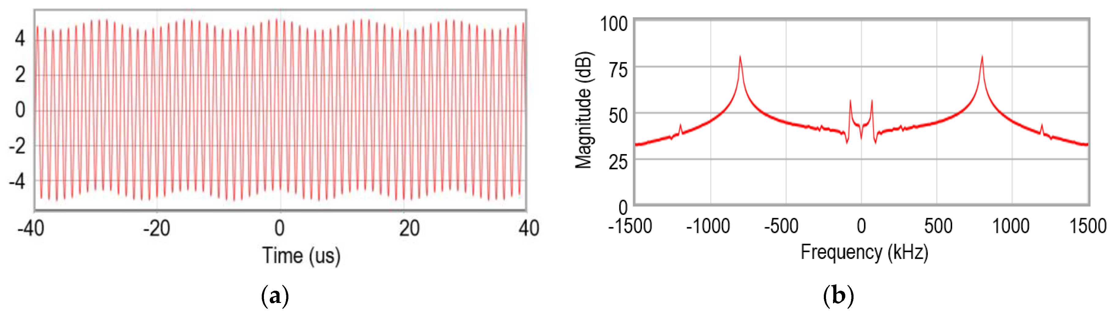
Figure 17a,b show magnitude in time domain and in frequency domain of VAB during power transmitting, respectively. Figure 17c,d show magnitude in time domain and in frequency domain of VAB after removing 70 kHz band signals, respectively. As shown in Figure 16, there are 800 kHz band signals and 70 kHz band signals during power transmitting, but the 70 kHz band signals are removed after using the filter. In this paper, however, the slotted Q factor method during power transmitting is used. A slot to detect MOs in the middle of the in-power is added to make it as less sensitive to the power of the transmitter coil as possible.

4. Conclusions

In this paper, we have presented a novel MOD method based on two-layer balanced coil array with serial-resonant Maxwell bridge circuits, which can detect even small MOs through high voltage change sensing. The balanced coil arrays are divided into two layers and placed one by one at each layer to reduce interference by the surrounding coils other than the MO to be detected. When a MOs are inserted, it is detected that the balance of the current induced in the two coils is broken. The smaller the size of the MO, the smaller the induced current difference. To solve this problem, we also proposed a Maxwell bridge circuit and serial-resonant capacitors, which result in a dramatically improved detection sensitivity. In the proposed system, the balanced coil arrays of the first and second layers have inductance of about 60 uH and 40 uH respectively, and serial-resonance Maxwell bridges have about approximately 100 Ω resistors and 1000 pF and 680 pF capacitors, respectively, for each layer. As a result of testing for 800 kHz AC generator, the proposed system can detect even coins and clips with a voltage difference of several hundred mV. It can be seen that the detection performance is improved compared to conventional circuits detecting MO with a difference of several uV~mV. In addition, the magnitude of the voltage is different depending on the location where the MO was placed, but it shows about 3 to 5 times larger than that without the MO. Therefore, the proposed method in this paper is expected to be useful as a MOD technology for high-power wireless charging with a distance of several tens of centimeters apart between the transmitter and receiver coils such as a robot or an electric vehicle.

5. Patents

Yongseok Lim, Haeyong Jung, and YongJu Park. Metal foreign object detection method in wireless power transmission. KR 10-2020-0111944.

Author Contributions

Conceptualization, S.K. and Y.L.; methodology, S.K., H.J. and Y.L.; software, S.K.; validation, H.J.; formal analysis, Y.J.; investigation, S.K. and Y.L.; resources, H.J.; writing—original draft preparation, S.K.; writing—review and editing, S.K and Y.L.; supervision, Y.L.; project administration, Y.L. All authors have read and agreed to the published version of the manuscript.

Funding

This work was supported by Institute for Information and Communications Technology Promotion (IITP) grant funded by the Korean Government (MSIP) (No. 2020-0-00148, development of ultra-compact/high efficiency wireless charging technology for 1 kW class robot).

Conflicts of Interest

The authors declare no conflict of interest.

References

  1. Yang, Y.; Cui, J.; Cui, X. Design and Analysis of Magnetic Coils for Optimizing the Coupling Coefficient in an Electric Vehicle Wireless Power Transfer System. Energies 2020, 13, 4143. [Google Scholar] [CrossRef]
  2. Seong, J.Y.; Lee, S.-S. A Study on Precise Positioning for an Electric Vehicle Wireless Power Transfer System Using a Ferrite Antenna. Electronics 2020, 9, 1289. [Google Scholar] [CrossRef]
  3. Wen, F.; Chu, X.; Li, Q.; Gu, W. Compensation Parameters Optimization of Wireless Power Transfer for Electric Vehicles. Electronics 2020, 9, 789. [Google Scholar] [CrossRef]
  4. TDK Developing Technologies, Achieves Wireless Power Transfer to Mobile Objects with High Efficiency Can Also Be Used for Rotating Parts Such as a Robot Arm. Available online: https://product.tdk.com/info/en/techlibrary/developing/wireless/index.html (accessed on 26 October 2020).
  5. Lim, Y.; Tang, H.; Lim, S.; Park, J. An Adaptive Impedance-Matching Network Based on a Novel Capacitor Matrix for Wireless Power Transfer. IEEE Trans. Power Electron. 2014, 29, 4403–4413. [Google Scholar] [CrossRef]
  6. Zhang, Y.; Yan, Z.; Zhu, J.; Li, S.; Mi, C. A review of foreign object detection (FOD) for inductive power transfer systems. eTransportation 2019, 1, 100002. [Google Scholar] [CrossRef]
  7. Gyun, W.D. Optimal Design and Control Strategy of Inductive Power Transfer Charging System for Electric Vehicles. Ph.D. Thesis, Sungkyunkwan University, Seoul, Korea, December 2015. [Google Scholar]
  8. Wireless Power Consortium. Foreign Object Detection. In Qi Wireless Power Transfer System Power Class 0 Specification; Parts 1 and 2: Interface Definitions, Version 1.2.3; Wireless Power Consortium: Piscataway, NJ, USA, 2017; pp. 127–139. [Google Scholar]
  9. Jeong, S.Y.; Kwak, H.G.; Jang, G.C.; Choi, S.Y.; Rim, C.T. Dual-Purpose Nonoverlapping Coil Sets as Metal Object and Vehicle Position Detections for Wireless Stationary EV Chargers. IEEE Trans. Power Electron. 2017, 33, 7387–7397. [Google Scholar] [CrossRef]
  10. Jeong, S.Y.; Thai, V.X.; Park, J.H.; Rim, C.T. Self-Inductance-Based Metal Object Detection With Mistuned Resonant Circuits and Nullifying Induced Voltage for Wireless EV Chargers. IEEE Trans. Power Electron. 2018, 34, 748–758. [Google Scholar] [CrossRef]
  11. Xiang, L.; Zhu, Z.; Tian, J.; Tian, Y. Foreign Object Detection in a Wireless Power Transfer System Using Symmetrical Coil Sets. IEEE Access 2019, 7, 44622–44631. [Google Scholar] [CrossRef]
  12. Zhou, B.; Liu, Z.Z.; Chen, H.X.; Zeng, H.; Hei, T. A New Metal Detection Method Based on Balanced Coil for Mobile Phone Wireless Charging System. In Proceedings of the International Conference on New Energy and Future Energy System, Beijing, China, 19–22 August 2016. [Google Scholar] [CrossRef] [Green Version]
  13. Maxwell’s Bridge. Available online: https://circuitglobe.com/maxwells-bridge.html (accessed on 30 October 2020).
Figure 1. The basic principle of transferring electric energy over the air.
Electronics 09 02070 g001
Figure 2. (a) The current and magnetic field generation, and (b) the equivalent circuit when a metallic foreign object (MO) is placed on the top of the coil.
Electronics 09 02070 g002
Figure 3. A cross-section of the system.
Electronics 09 02070 g003
Figure 4. A two-layer balanced coil array architecture. (a) Balanced coil array in the first; (b) balanced coil array in the second layer; and (c) overlapped layers to cover the entire plane.
Electronics 09 02070 g004
Figure 5. Maxwell bridge circuits.
Electronics 09 02070 g005
Figure 6. Structure that combines a balanced coil array and Maxwell bridge circuits.
Electronics 09 02070 g006
Figure 7. Proposed Maxwell bridge circuit with serial-resonance capacitors.
Electronics 09 02070 g007
Figure 8. Proposed system and test environment.
Electronics 09 02070 g008
Figure 9. Metal foreign objects used in the experiment.
Electronics 09 02070 g009
Figure 10. (a) Coordinates to indicate the position of the coin and the zero-to-peak value of VAB measured at each position, and (b) the balanced coil set and the position of the loop coil belonging to the set.
Electronics 09 02070 g010
Figure 11. Quality factor of the serial resonant circuit according to resistances.
Electronics 09 02070 g011
Figure 12. VAB of the Maxwell bridge (a) when R1 and R2 do not match and (b) when C1 and C2 do not match.
Electronics 09 02070 g012
Figure 13. Voltage difference between when Maxwell bridge is used and when not used. (a) When a 500 KWN coin is at (x1, y1), and (b) at (x1, y2).
Electronics 09 02070 g013
Figure 14. VAB according to MO’s position (a) MO position in a balanced coil, (b) measured VAB.
Electronics 09 02070 g014
Figure 15. Experimental environment to test the effect between the wireless power transfer operation and the metal object detection (MOD) operation.
Electronics 09 02070 g015
Figure 16. Measured voltages, VA, VB, and VAB at 7 cm apart in powering.
Electronics 09 02070 g016
Figure 17. Magnitude of VAB (a) in time domain and (b) in frequency domain during power transmitting (70 kHz + 800 kHz), and (c) in time domain and (d) in frequency domain after removing 70 kHz band signals.
Electronics 09 02070 g017aElectronics 09 02070 g017b
Table 1. Comparison of metal foreign objects used in the experiment.
500 KRW Coin10 KRW CoinClipScrew
sizediameter 2.65 cmdiameter 1.8 cm3.5 cm × 0.8 cm0.5 cm × 0.5 cm × 1.2 cm
weight
(component)
7.9 g
(copper 75%, nickel 25%)
1.2 g
(copper 48%, aluminum 52%)
--
Table 2. Measured VAB for various MOs.
no MO500 KRW Coin10 KRW CoinClipScrew
VAB(zero-to-peak)0.1971.10.6750.30.249
Table 3. VAB according to MO’s position.
Without MOabcde
B(X1, X6) (V)0.1971.10.6750.3010.190.187
B(Y1, Y4) (V)0.0950.060.0960.180.30.68
Table 4. Measured VAB_peak_to_peak and VENV_70k according to distance between the transmitter and receiver coils.
No Powering3 cm Apart in Powering5 cm Apart in Powering7 cm Apart in Powering
VAB_peak_to_peak1.4 V1.5 V1.5 V1.6 V
VENV_70k1.4 V2.8 V3.3 V4.9 V
Publisher’s Note: MDPI stays neutral with regard to jurisdictional claims in published maps and institutional affiliations.

