1. Introduction
Power-combining techniques are widely used in the design of power amplifiers (PAs) to sum the power from individual linear PAs.
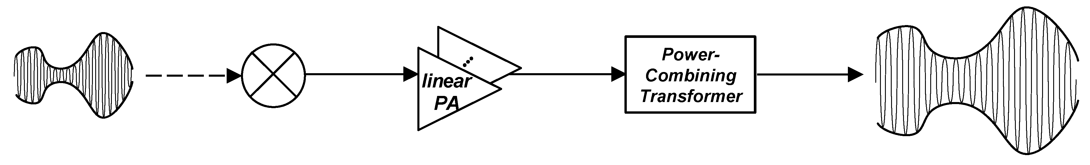
Figure 1 shows a block diagram of a radio frequency (RF) transmitter, including a PA with a power-combining transformer. For on-chip power-combining techniques, many studies have used power-combining transformers, such as series-combining transformers (SCTs) and parallel-combining transformers (PCTs) [
1,
2,
3,
4,
5].
A PA is a major consumer of power in an RF transceiver. Thus, there has been increasing demand for studies on PA structures to increase battery lifetime. One promising approach is outphasing, which is also known as linear amplification using nonlinear components [
6,
7,
8,
9,
10,
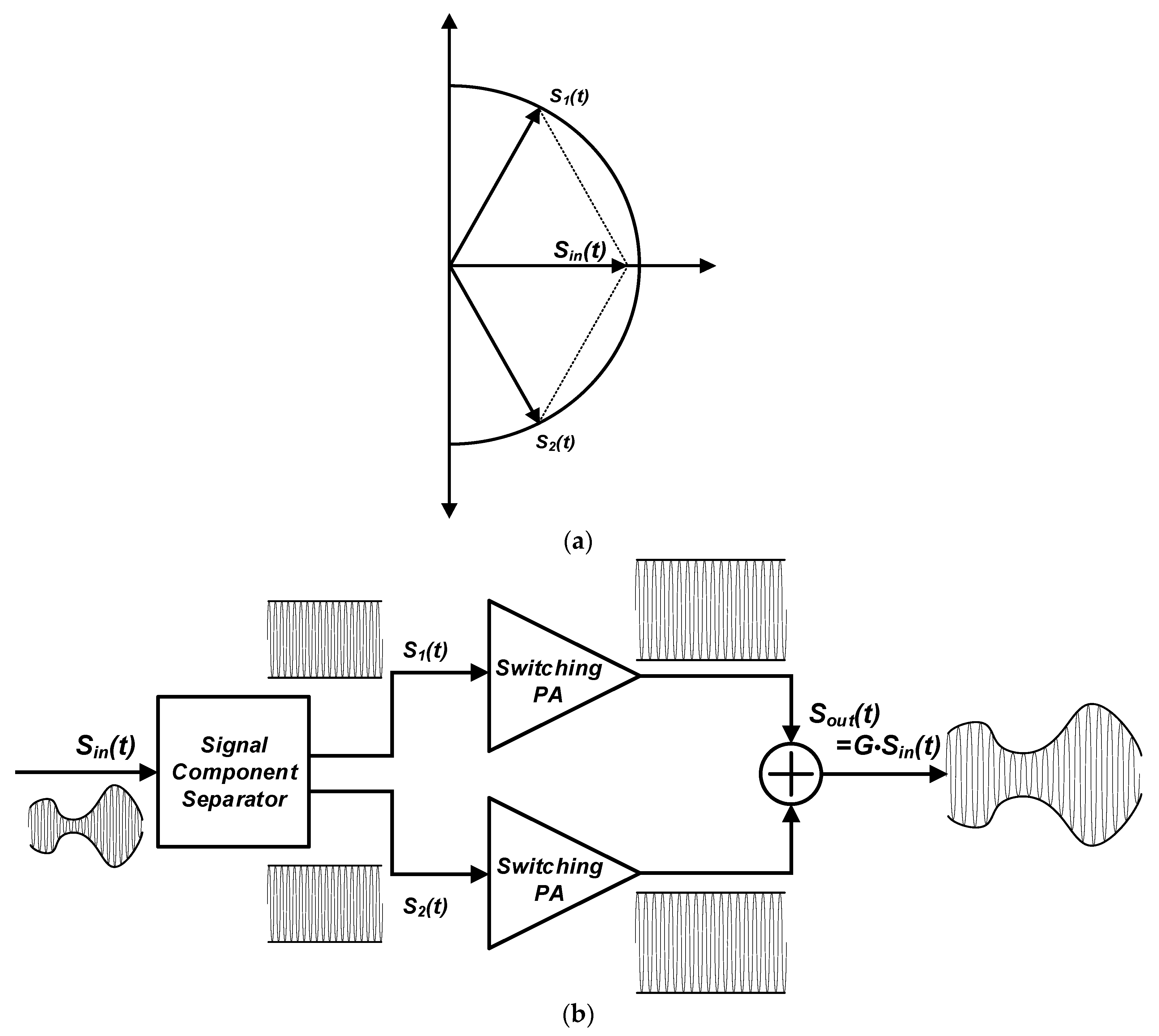
11]. In an outphasing system, two constant amplitude signals in an outphasing PA can be combined using isolation or non-isolation power combiners, as shown in
Figure 2. An isolation combiner [
12], such as a Wilkinson combiner, provides good linearity because there is less interaction between two adjacent PAs. However, it has poor efficiency because the RF power is wasted when the phase angle of the outphasing signals is large. In contrast, a non-isolation combiner reduces the power dissipation by improving the wasted power in the combined outphasing signal. However, conventional non-isolation combiners typically require bulky quarter-wave transmission lines, which are difficult to integrate on a chip [
13].
SCTs and PCTs can combine several individual amplifiers to increase the output power level, but only the SCT structure has been used for on-chip non-isolation outphasing PAs [
14,
15,
16]. However, a PCT is typically much smaller than an SCT. When a PCT is incorporated in the circuit design, the required die area can be reduced compared with that of an SCT.
In this paper, we analyze the outphasing operation for SCT and PCT power-combining transformers, and propose a compact on-chip outphasing PA with a PCT. By analyzing SCT and PCT power-combining transformers with non-ideal transformer models as outphasing combiners, we verify that the outphasing summation property can be obtained with a smaller die area by using the PCT structure. In addition, we analyze the outphasing operation of class-D PAs with an outphasing combiner using an SCT or PCT. A tuning inductor method is also proposed to improve the performance in out-of-phase mode.
This paper is organized as follows.
Section 2 shows the analysis of the SCT and PCT as outphasing combiners and system simulation results using non-ideal SCT and PCT models. In
Section 3, the analyses for the outphasing operation of transformers and class-D switching PAs are described, and a tuning inductor method is presented.
Section 4 explains the circuit design. The measured results are discussed in
Section 5, followed by the conclusion in
Section 6.
2. Outphasing Combiner Using Power-Combining Transformers
Figure 2 illustrates the basic outphasing principle of the operation and outphasing PA architecture. The amplitude and phase modulated signal
can be separated into two constant-amplitude phase modulated signals:
where
,
is the angular frequency,
is the amplitude of the signal of
,
is the phase of the signal of
, and
is the maximum value of
. The amplitude information of
is translated into the outphasing angle
by the following equation:
The amplitude and phase modulated input signal
is decomposed into two constant-amplitude phase modulated signals,
and
. Thus, switching PAs can be used to amplify
and
, as shown in
Figure 2. The two amplified signals from the two switching PAs are summed through an outphasing combiner to reconstruct the original signal with increased amplitude. To reconstruct the desired signal properly through the outphasing combiner, the condition of Equation (3) must be met for the amplitude of the combined signal. Thus, the summation property can be achieved when the amplitude through the output combiner is proportional to
[
14,
15].
Isolation or non-isolation combiners can be used for outphasing combiners. An isolation combiner such as a Wilkinson combiner typically has low efficiency, so non-isolation combiners are widely used to achieve high efficiency. Transformer-based combiners have been applied as on-chip outphasing combiners because of the useful characteristics of a typical transformer, such as impedance matching, DC isolation, and signal summation. However, in previous research, only SCTs have been used for on-chip outphasing combiners, and their operation was analyzed with an ideal model of a transformer [
14,
15].
In this work, the operations of SCTs and PCTs as outphasing combiners are analyzed with non-ideal models of the transformer.
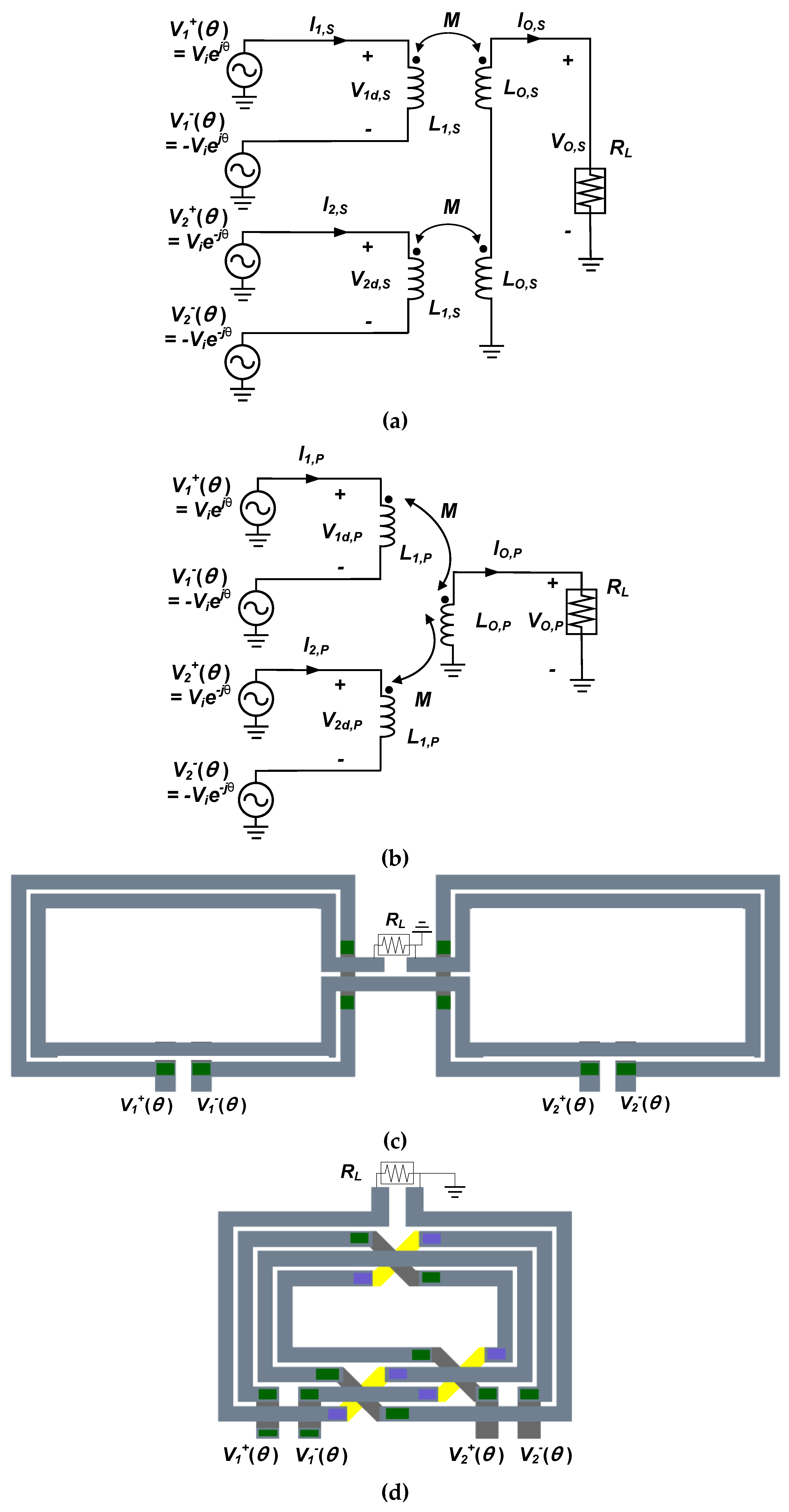
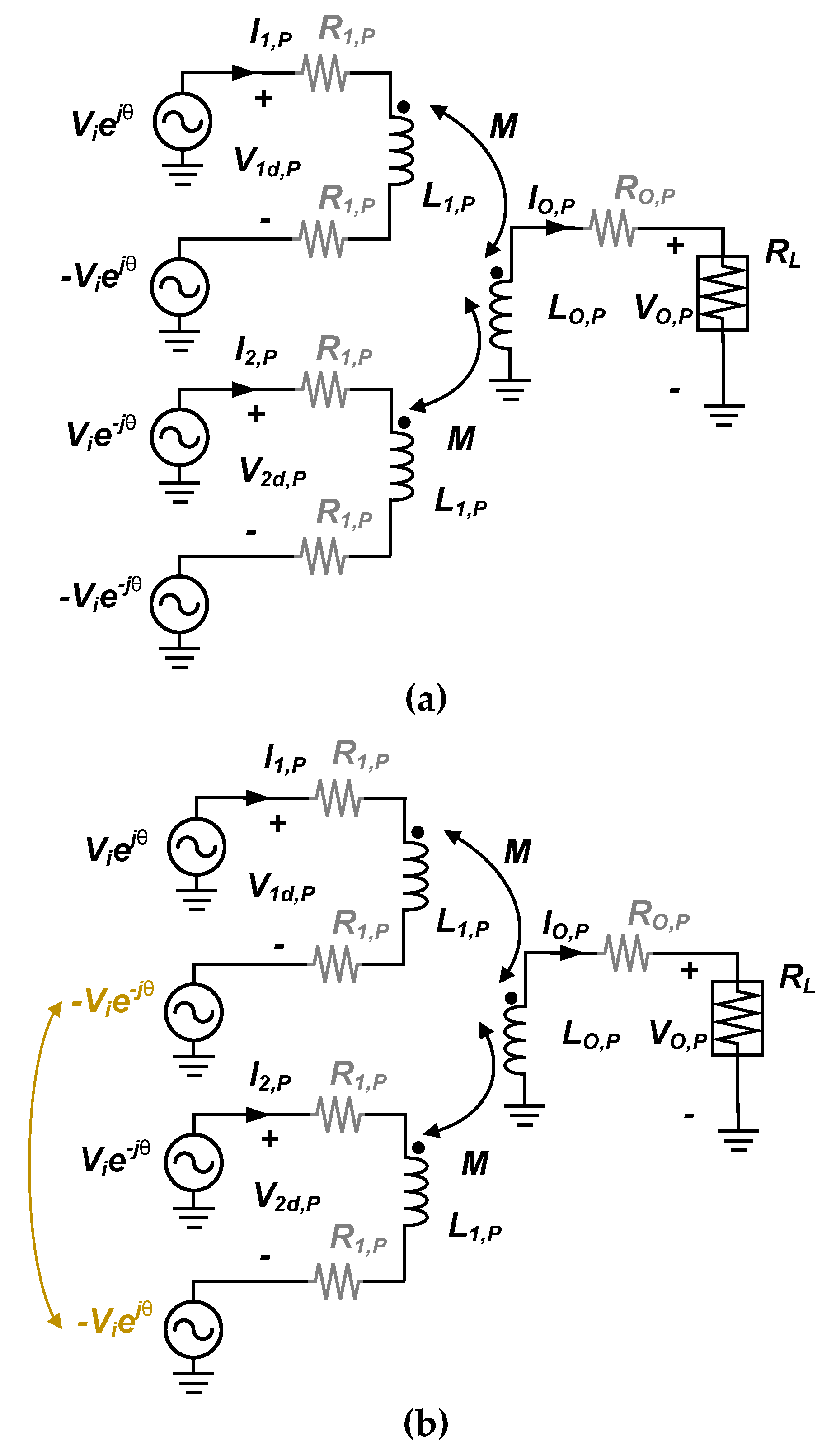
Figure 3a shows an SCT with an equivalent non-ideal model. The operations of the outphasing combiner with switching PAs are also shown in
Figure 3a, where the output signals of class-D PAs are modeled as voltage sources. The operation of class-D or class-F PAs is less sensitive to load variation [
17,
18,
19], so they are preferred for outphasing PAs when considering linearity performance. A class-F PA requires multiple bulky resonant circuits, so class-D PAs are widely used for on-chip outphasing PAs [
14,
15,
16].
The input voltages of the outphasing combiner are
and
, where
is the outphasing angle. For the differential case, the input voltages of the combiner are
,
,
, and
. As shown in
Figure 3a, the voltage differences between the positive and negative parts of the primary winding are:
In the case of an SCT with the equivalent lumped model, the voltages at the primary and secondary windings are:
Using Equations (4), (5), and (6), the following relationship can be found:
The relation for the output current can be derived from Equations (6) and (7) thus:
The output voltage at the secondary winding is:
The output voltage is proportional to , and the outphasing summation property is satisfied. The desired signal can be reconstructed through the SCT combiner.
In the case of a PCT with an equivalent lumped model, as shown in
Figure 3b, the voltages at the primary and secondary windings are:
The relation for the output current can be derived from Equations (4), (10), and (11) thus:
The output voltage at the secondary winding is:
Thus, the outphasing summation property can be obtained using the PCT structure as well.
Example layouts for the SCT and PCT cases are shown in
Figure 3c,d to compare their required die areas. The sizes of the layouts for the SCT and PCT are 0.425 × 1.6 mm and 0.425 × 0.715 mm, respectively. Because a PCT is typically much smaller than an SCT, the required die area can be reduced by using a PCT as an outphasing combiner.
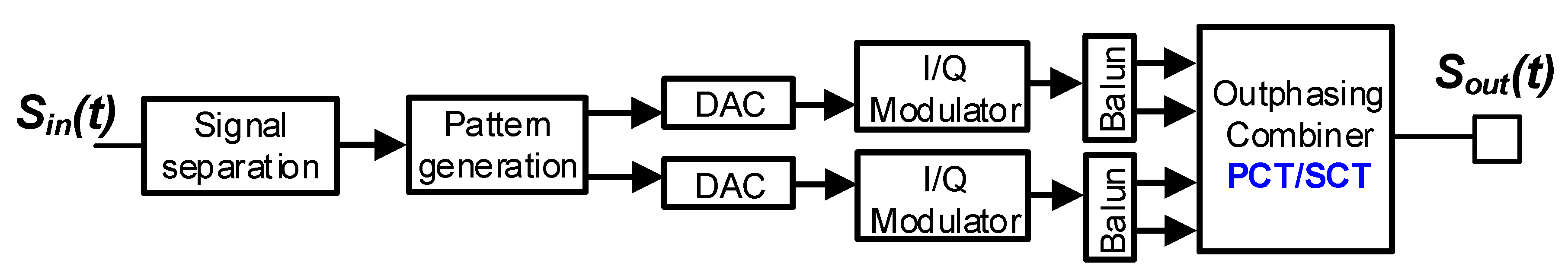
Simulations are performed using an Advanced Design System (ADS) to verify their outphasing operation. A diagram of the simulation setup is shown in
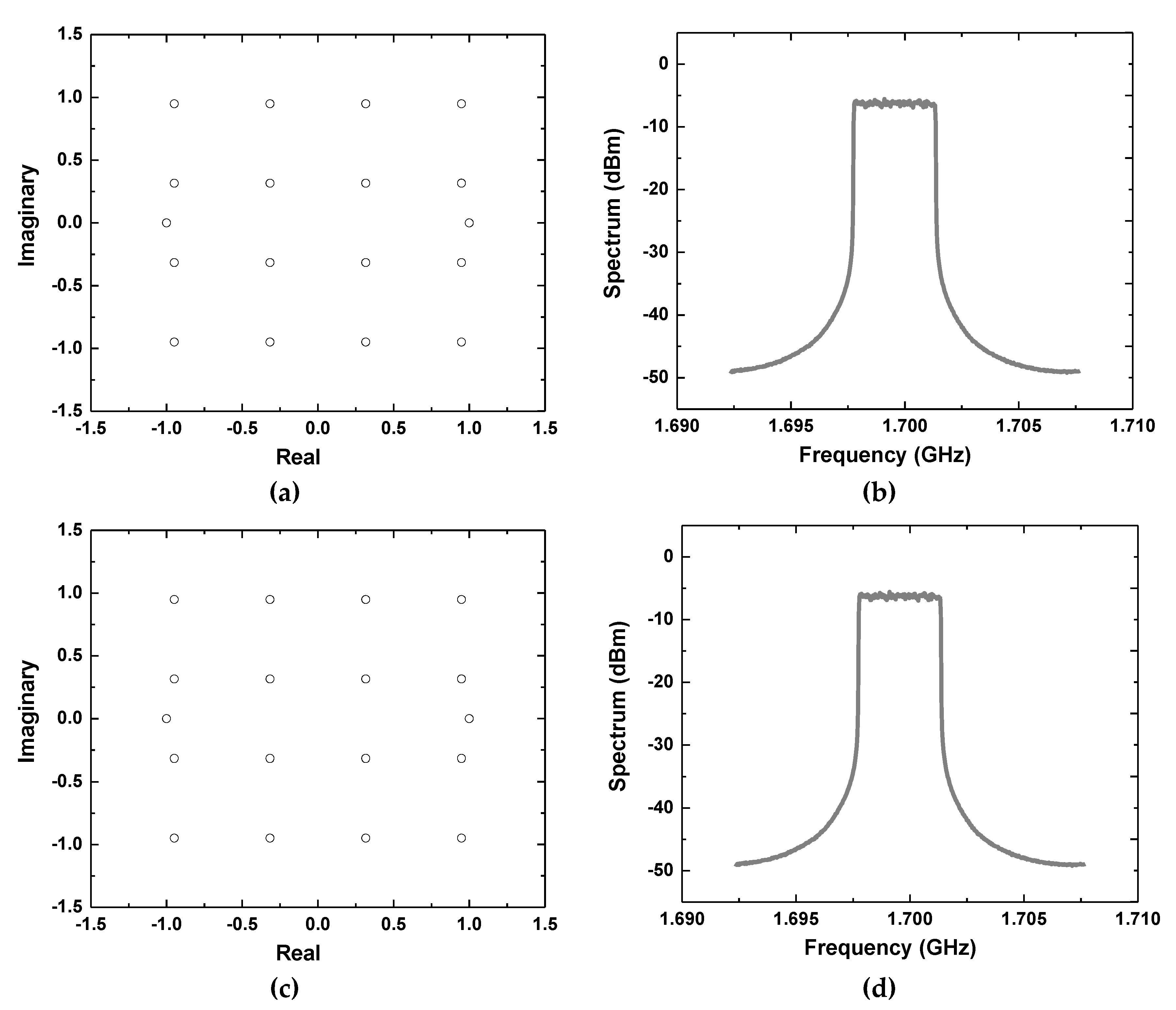
Figure 4. A 16QAM OFDM signal is separated in MATLAB, and the separated outphasing signals are incorporated in the ADS simulation. Four outphasing signals are generated using the ideal balun, and an output signal is obtained with non-ideal SCT or PCT models. The simulated output constellations and spectrums are shown in
Figure 5 for the SCT and PCT. Because the outphasing summation property can be obtained using both the SCT and PCT combiners, the desired ideal signals are reconstructed for both cases.
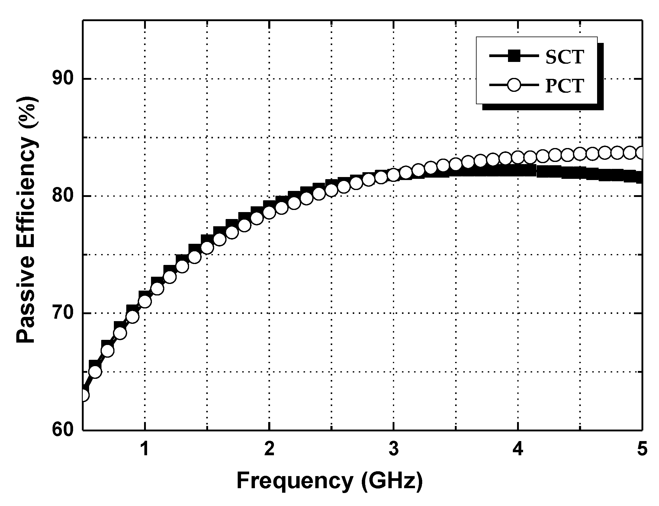
To evaluate the passive efficiencies of the SCT and PCT cases, electromagnetic (EM) simulations were performed using the ADS momentum for the example layouts in
Figure 3. For the design of the SCT and PCT, a 3.4 μm thick Cu top layer was used. The efficiencies of the SCT and PCT cases are compared in
Figure 6. The efficiency of the PCT case is similar to that of the SCT case in the frequency range of 1.7–2 GHz.
4. Circuit Design
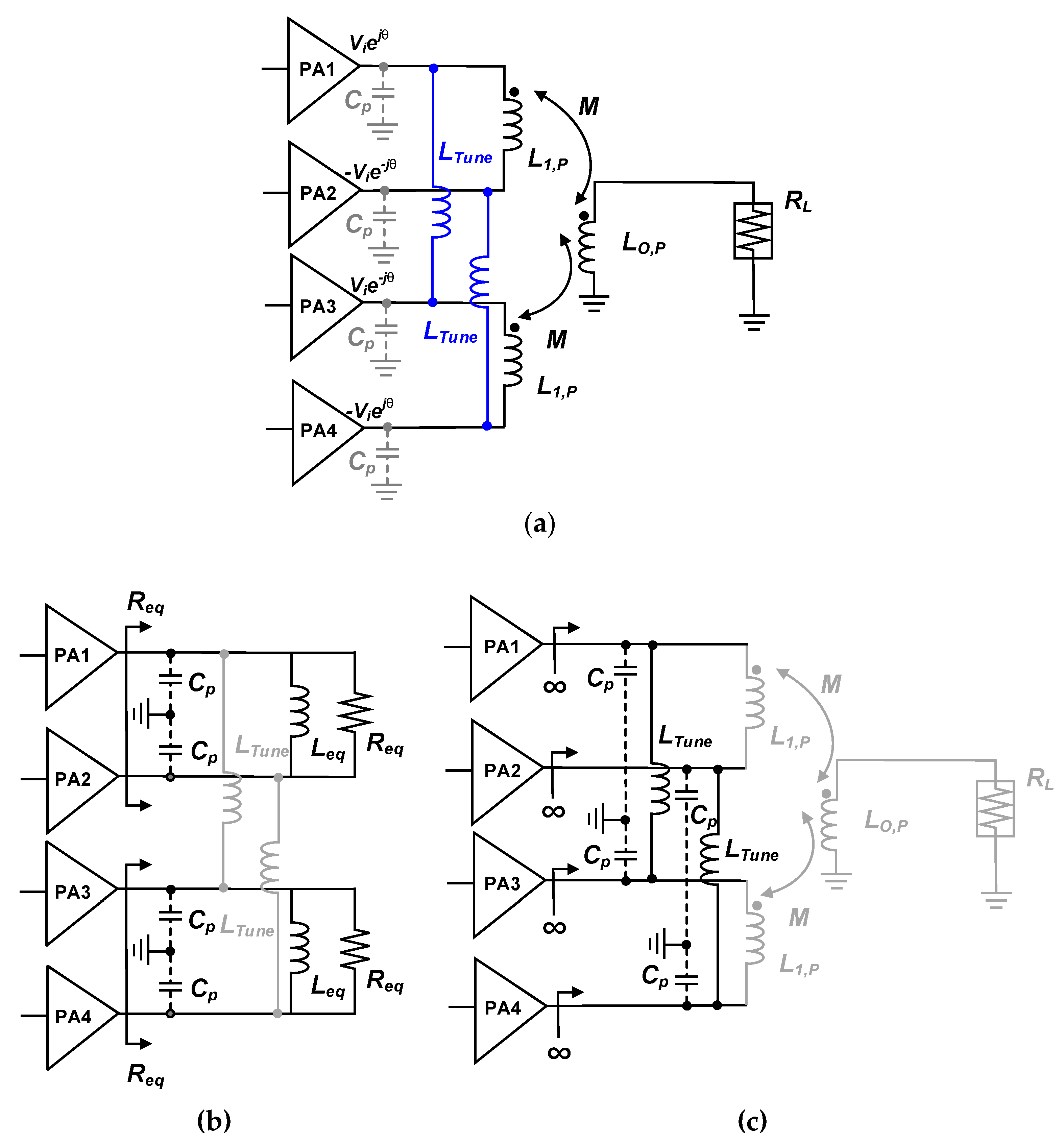
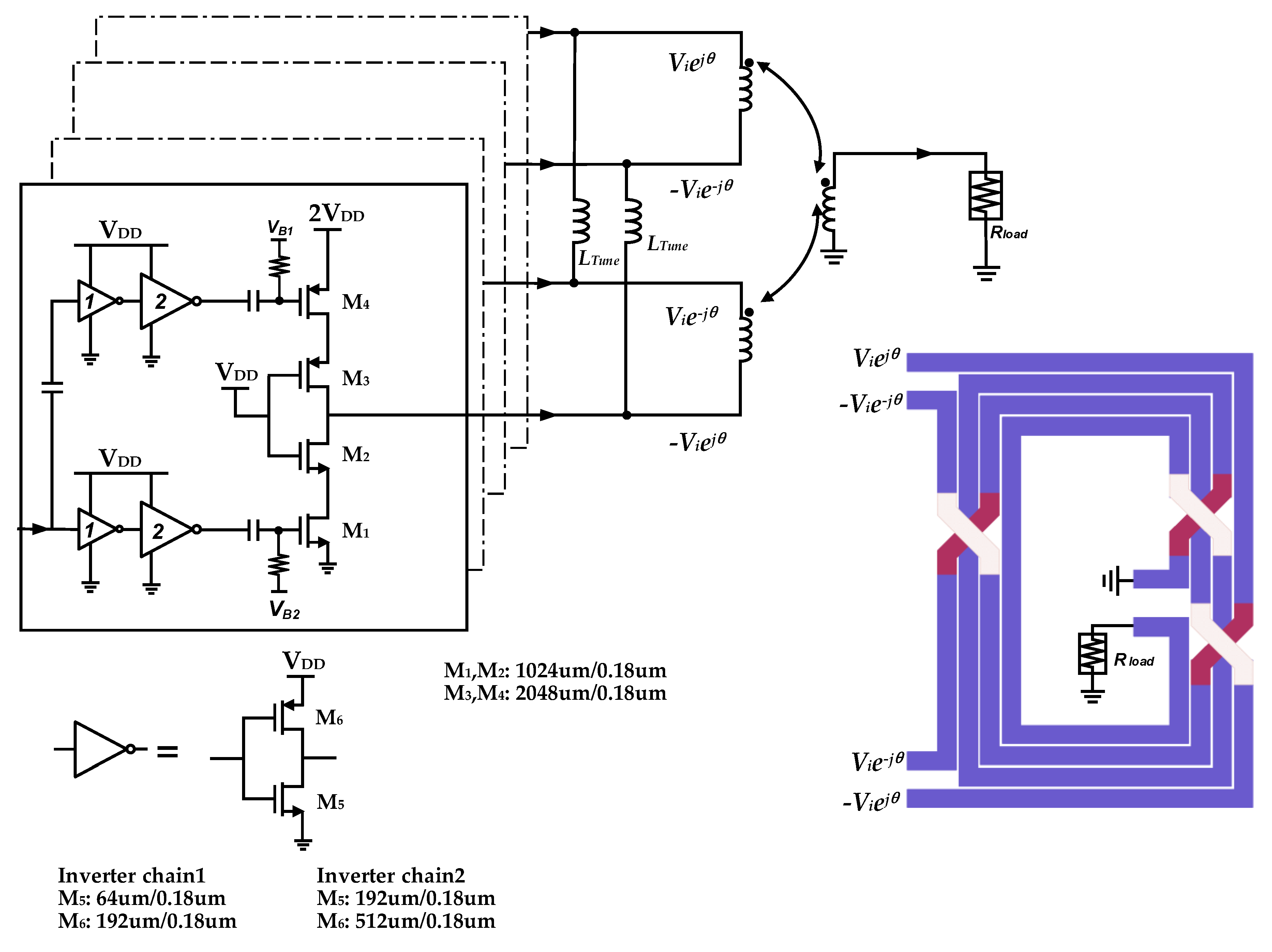
To implement a compact outphasing CMOS PA, a PCT outphasing combiner is designed.
Figure 9 shows the layout of the PCT. The size of the PCT is 0.745 × 0.515 mm
2. Transformers are designed with a 2.34 μm thick Al top metal layer in a standard 0.18 μm CMOS process. The transformer windings use 30 μm wide lines and 5 μm spacing. A turn ratio of 1:2 is selected to provide impedance transformation. Because all primary and secondary windings are concentrated in a smaller space, the size of the PCT can be much smaller than that of the SCT. To estimate its performance, EM simulations are performed using the ADS momentum. The simulated inductances of each primary winding and secondary winding are 1.35 nH and 3.25 nH, respectively, at 1.7 GHz. The EM simulated PCT achieves a coupling factor of 0.71.
The proposed outphasing system is designed with four class-D PAs using the proposed PCT.
Figure 9 also shows a simplified schematic of the class-D PA and its associated circuits, including the inverter chain. The four outphasing PAs are connected to positive or negative parts of the two primary windings of the PCT. A cascoded inverter-based class-D PA using thin-gate devices is designed using a 3.6 V supply. Thin-gate devices of L = 0.18 μm are used to minimize on-resistance as well as parasitic capacitances of the transistor. To increase output power from each unit class-D PA, the cascoded inverter topology is adopted, which allows an output voltage swing of twice the nominal supply voltage (V
DD = 1.8 V). The transistor widths of NMOS (M
1/M
2) and PMOS (M
3/M
4) on each unit class-D PA are 1024 μm and 2048 μm, respectively, as shown in
Figure 9. Each inverter chain operates with a 1.8 V supply.
The two tuning inductors shown in
Figure 9 are added between the drains of two class-D PAs to improve the back-off efficiency. The EM simulated tuning inductance,
, is 2.15 nH at 1.7 GHz.
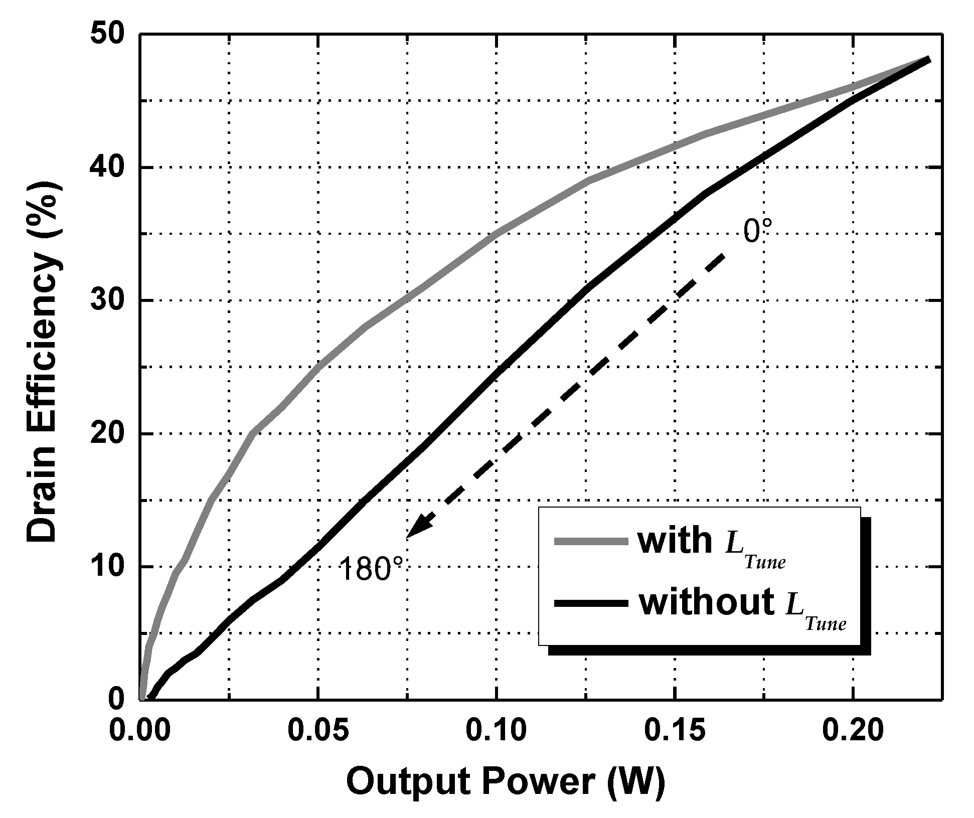
Figure 10 shows the simulated efficiency versus output power with and without tuning inductors. An EM simulated transformer model is used for the circuit simulations. The results show that the proposed PA, with tuning inductors, improves the efficiency performance by approximately 10% at the 6-dB back-off level (55-mW output power) of the output power.
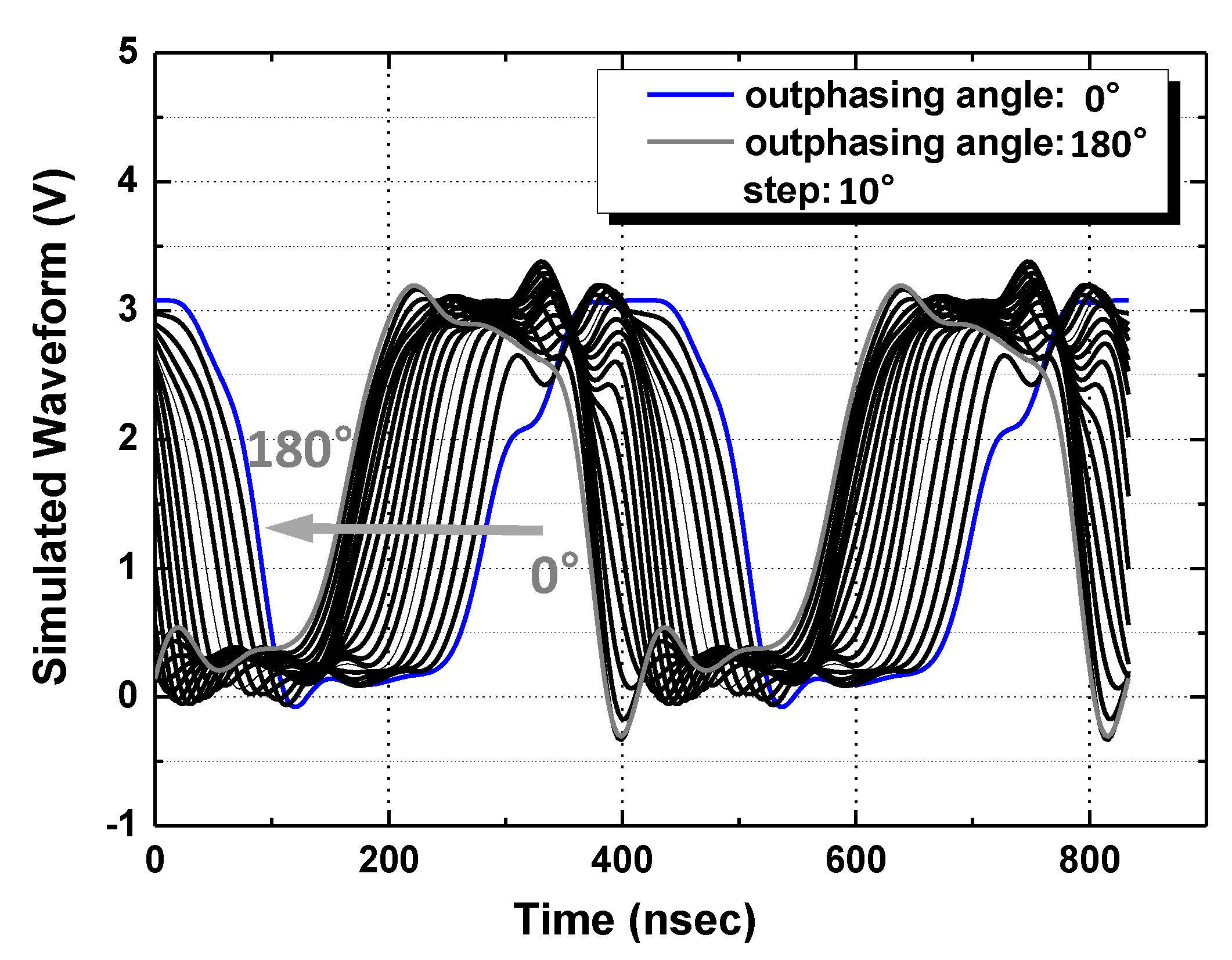
Figure 11 shows the simulated output voltage waveforms of each class-D PA. The simulated voltage waveforms of the class-D PAs are not degraded with the variation of the outphasing angle because of the tuning inductor method. Thus, the efficiency performance can be higher when the outphasing angle is increased, as shown in
Figure 10.
5. Measurement Results
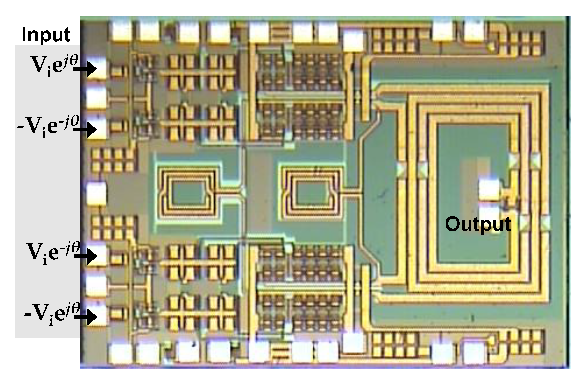
To verify its operation of the proposed outphasing CMOS PA using the compact PCT with a tuning inductor method, a fully integrated outphasing CMOS PA was fabricated using a standard 0.18 μm CMOS process. A die photograph of the implemented PA is shown in
Figure 12. The chip area is 1.2 × 1.6 mm
2, including the input and output PADs.
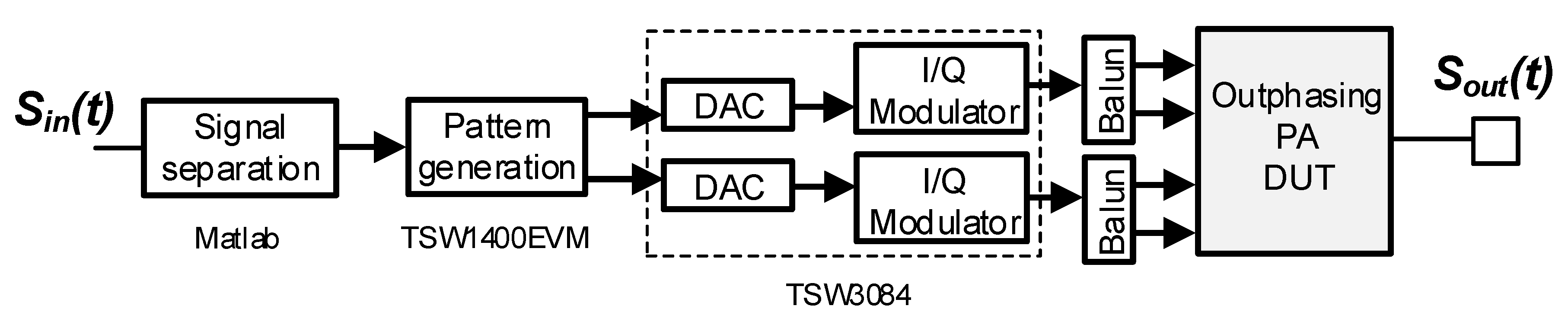
The signal decomposition into
and
was performed using MATLAB, as shown in
Figure 13. The decomposed data were downloaded into a pattern generator and fed to a dual-RF channel TSW3084 board with digital-to-analog converters (DAC3484) [
20,
21]. To generate the differential signals, external baluns (BALH-0006) were used. Thus, two differential RF signals (
,
were applied to the test chip. The offset of the path mismatch between the paths for
and
was measured with a signal analyzer, and corrections for the offsets were applied to the pattern generator.
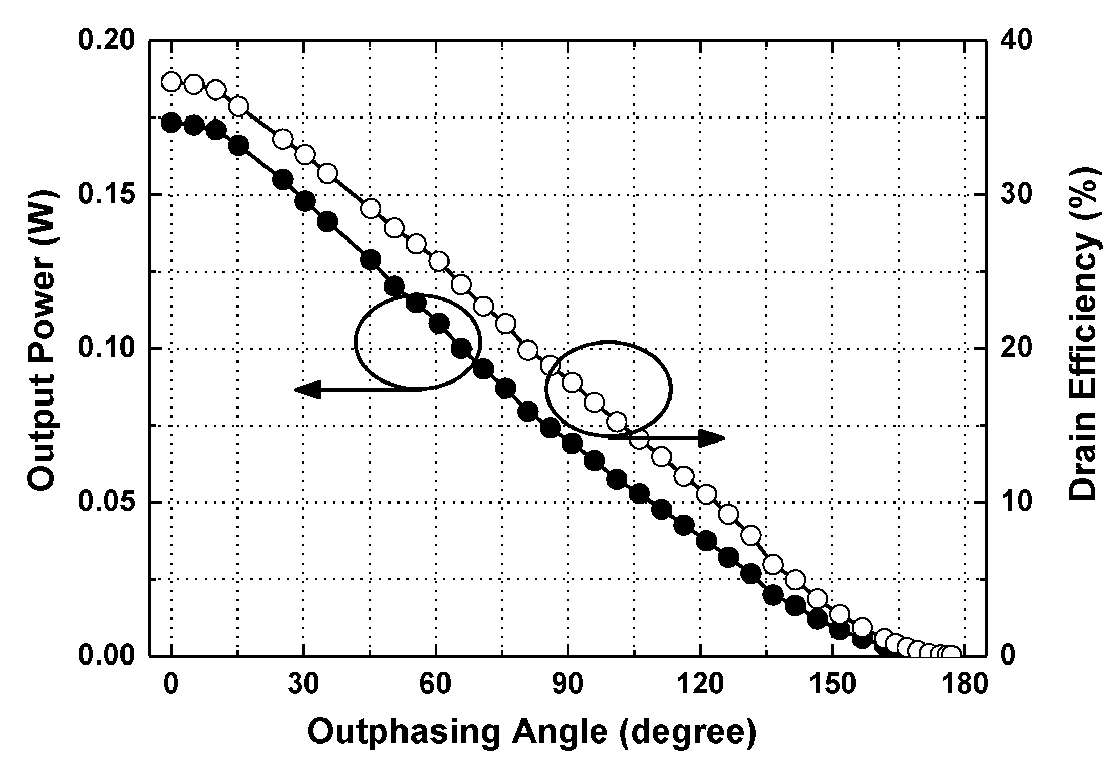
Figure 14 shows the measured output power and drain efficiency (DE) according to the outphasing angle variation at 1.7 GHz. A maximum DE of 37.3% was achieved with an output power of 173 mW (22.4 dBm) with V
DD = 1.8 V and 2V
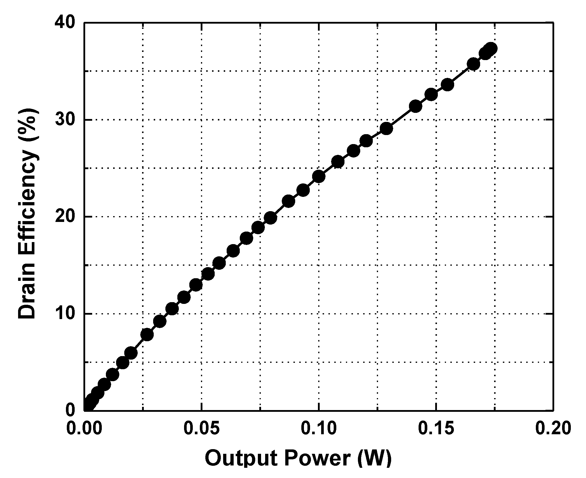
DD = 3.6 V. The DE is defined as output power divided by DC power consumption of the final class-D PA stage. The measured DE versus output power is shown in
Figure 15. The maximum power-added efficiency (PAE) was 26.5%, where the PAE is defined as output power divided by the DC power consumption of the final class-D PA stage and all inverter chains. The measured PAE is approximately 10% lower than DE in this work, but that is caused by the non-optimization of the two-stage inverter chain. In addition, the device size of the inverter chain using a 0.18 μm CMOS process will be larger than other works using a nanometer CMOS process, resulting in the large driving loss. If it is well-optimized further, and implemented using a nanometer CMOS process, PAE can be readily improved.
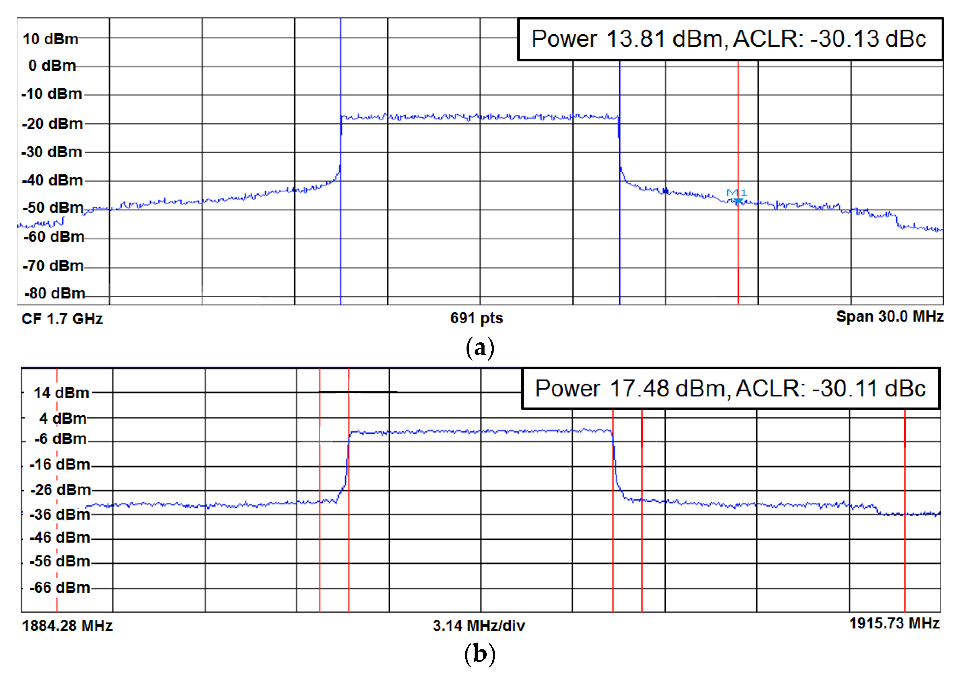
A modulated signal measurement was performed with a long-term evolution (LTE) signal with 10 MHz bandwidth, as shown in
Figure 16. Without a digital pre-distortion (DPD) applied, the adjacent channel leakage ratio (ACLR) of the proposed outphasing PA was obtained at less than −30 dBc, up to 13.81 dBm, with a 2V
DD of 3.6 V. Because the summation property can be obtained using the PCT outphasing combiner, the output signal was properly reconstructed. To check the capability of wide-frequency operation, the LTE signal was also tested at 1.9 GHz. By increasing the supply voltage, the linear output power could be increased. An ACLR of less than −30 dBc was obtained at up to 17.48 dBm, with 2V
DD = 3.8 V at 1.9 GHz.
Table 1 shows a comparison of this work with state-of-the-art outphasing CMOS PAs. The implementation methods of outphasing combiners are also indicated in
Table 1. In [
21,
22], off-chip baluns and multiple inductors and capacitors are required for the construction of the outphasing combiners, and thus the outphasing combiners were implemented using off-chip lumped elements on the printed circuit boards (PCBs). In [
14], an additional off-chip output balun is required on the PCB, and its loss was de-embedded during the measurement procedure. For fully integrated outphasing combiners, only SCT structures have been previously used [
15,
16]. In this work, a CMOS outphasing combiner that uses a PCT structure is proposed. In addition, the PCT structure, in its role as an outphasing combiner, is analyzed using non-ideal transformer models and verified with measurement results. Because the PCT structure can be approximately half the size of the SCT, as shown in
Figure 3, an implemented outphasing combiner using a PCT structure can save the required die area. Among the CMOS outphasing PAs using fully integrated outphasing combiners, the size of the outphasing combiner in this work is much smaller than those in other works.


 and
and 


