Article

A 28 GHz Linear Power Amplifier Based on CPW Matching Networks with Series-Connected DC-Blocking Capacitors

1
High-Frequency High-Voltage Device and Integrated Circuits R&D Center, Institute of Microelectronics, Chinese Academy of Sciences, Beijing 100029, China
2
School of Microelectronics, University of Chinese Academy of Sciences, Beijing 100029, China
*
Author to whom correspondence should be addressed.
Electronics 2020, 9(4), 617; https://doi.org/10.3390/electronics9040617
Submission received: 14 March 2020 / Revised: 3 April 2020 / Accepted: 4 April 2020 / Published: 6 April 2020
(This article belongs to the Special Issue CMOS Power Amplifier Design and Applications)

Abstract

:
In this paper, the influence of the DC-blocking capacitors leveraged in coplanar waveguide (CPW) matching networks is studied. CPW matching networks with series-connected DC-blocking capacitors are less sensitive to capacitance and are adopted in a 28 GHz power amplifier (PA). The PA targeting fifth-generation (5G) phased array is developed in 90 nm silicon-on-insulator complementary-metal-oxide-semiconductor (SOI CMOS) technology. A stacked field-effect-transistor (FET) architecture is elected in the output stage to boost the output power and reduce the die area. The PA with a core area of 0.31 mm2 demonstrates a maximum small signal gain of 13.7 dB and a −3 dB bandwidth of 6.3 GHz (22.9–29.2 GHz). The PA achieves a measured saturated output power (Psat) of 14.4 dBm and a peak power added efficiency (PAE) of 25% for continuous wave signals. At 24/25.6/28 GHz, the PA achieves +7.87/+9.16/+10.7 dBm measured output power and 6.21%/8.11%/10.17% PAE at −25 dBc error vector magnitude(EVM) for a 250 MHz-wide 64-quadrature amplitude modulation (64-QAM). The developed linear PA provides a great potential for low-cost 5G phased array transceivers.

1. Introduction

The fifth generation (5G) communication technology provides a great potential for numerous emerging applications, such as broadband data traffic, augmented reality (AR), internet of things (IOT), internet of vehicles (IOV), etc. Because of the wide available bandwidth, the mm-Wave technique will play a key role in these emerging demands to achieve multi-gigabit-per-second data rates [1,2,3]. Figure 1a shows the spectra proposed by different regions in the world for 5G service, and frequency bands allocated around 28 GHz are one of the most promising candidates [4,5]. Moreover, the spectral efficiency and link range can be further improved by massive multiple-input multiple-output (MIMO) and phased array techniques. As an example of a transmitter front-end shown in Figure 1b, numerous power amplifier (PA) cells with integrated phase shifters are required to provide medium power amplification for high-order quadrature amplitude modulation (QAM) signals and achieve accurate beam control. Consequently, PAs with compact size, wide bandwidth, high linearity, and low cost are always desirable for 5G applications.
Mm-Wave PAs in CMOS technology is well suited for fully integrated 5G phased array transceivers due to low cost and high integrity. To date, significant progress in this field has been made [5,6,7,8,9]. However, the high substrate-induced loss is still a critical challenge for mm-Wave circuits in bulk Si CMOS, which limits the gain and the power efficiency of the PA [6]. SOI-CMOS technology featuring high resistance silicon substrate (>1000 Ω) is one of the feasible solutions for low-loss mm-Wave circuits [10,11].
In Reference [5] and [6], the K-band matching networks are designed by transformers and metal–oxide– metal (MOM) capacitors, and the capacitors are carefully simulated and measured to evaluate the influence. The coplanar waveguide (CPW) technique with DC-blocking capacitors only is widely used in mm-Wave applications [12,13,14,15]. Generally, the DC-blocking capacitor features a relatively large size and severe parasitic effects, which in turn lead to a low self-resonance frequency and a low quality factor (Q-factor). In addition, DC-blocking capacitors are usually not considered in the Smith chart, especially when the capacitors are connected with the paralleled CPW lines, and lower down the prediction accuracy of the simulation. Consequently, the study of DC-blocking capacitors in CPW matching networks is of great significance, which has not been reported.
In this paper, the influence of the DC-blocking capacitors in CPW matching networks is studied. Simulation results indicate that the CPW matching networks with series-connected DC-blocking capacitors are less sensitive to the capacitance and are adopted in a 28 GHz single-end PA in 90 nm SOI-CMOS technology. A 2-stacked-FET architecture is utilized in the output stage to boost the output power and reduce the die area. The developed compact PA demonstrates high linearity.

2. Design of the Linear PA

2.1. CPW Matching Networks with DC-Blocking Capacitors

Lumped components such as inductors and capacitors are widely adopted in RF circuits based on CMOS technologies [16,17]. A great deal of efforts has been made by researchers to get an accurate model of lumped inductors and metal–insulator–metal (MIM) capacitors for the implementation in RF circuits [18,19]. However, the parasitic effects of passive components in the mm-Wave band are still a critical challenge. The large MIM capacitors fabricated in the CMOS process usually feature low self-resonance frequencies, and the Q-factor of capacitor is inversely proportional to the operation frequency [20]. Consequently, distributed structures like CPW lines and microstrip (MST) lines are preferred in mm-Wave circuits. In Figure 2a, the cross-section of the 90 nm SOI CMOS technology is depicted. Five metal layers are fabricated for the back end of line (BEOL). An LTD substrate file with all material parameters and surface impedance of the conductor materials defined is provided by foundry for electro-magnetic (EM) simulation. In this work, an MST line is designed by one top thick metal layer (ME) and one thin metal layer (M1). A CPW line is designed by a top thick metal layer (ME). The thickness of the high-resistance silicon substrate is 300 μm. In Figure 2a, a simulation setup for CPW line and MST line is also illustrated. The s2p files of transmission lines are gained from carefully performed EM simulations, and the impedance of port1 and port2 is standard 50 Ω.
In this paper, the electro length of the transmission lines is defined as λ, and the simulated length of a 50 Ω λ/4 CPW line at 26 GHz is 1.278 mm, which is only 4/5 of the length of a λ/4 MST line. Consequently, compact matching networks can be realized by CPW lines. The simulated results in Figure 2b indicate that the MST line features large parasitic capacitance, and high insertion loss is observed in Figure 2c. Finally, the characteristic impedance of the CPW lines can be tuned by the width of the signal line and the space between the signal line and the ground plane, which is more flexible than the MST lines, which can only be tuned by the width of the signal line. In this paper, CPW lines are adopted for matching networks.
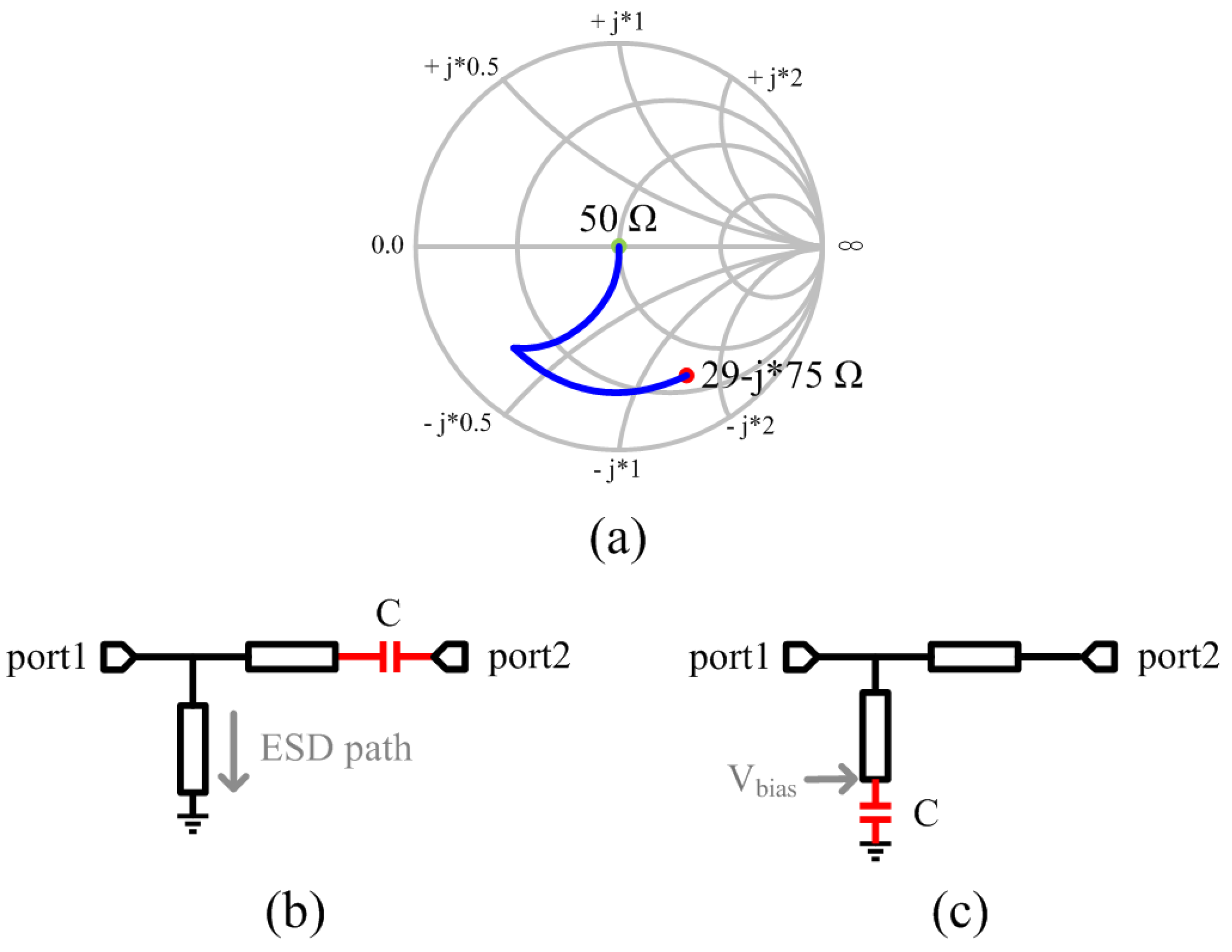
CPW lines connected in series or in parallel are two types of the most used structures in matching networks. As is shown in Figure 3a, a CPW matching network is designed in a Smith chart to achieve a conjugate matching between the source impedance and the input impedance of the developed PA, which are 50 Ω and 29 − j*75 Ω, respectively. The network comprises a shorted CPW line and a series CPW line. One capacitor is needed to achieve DC isolation in the input matching network, which is not used for matching. As is depicted in Figure 3b,c, DC-blocking capacitors can be applied in two methods. The capacitor implemented in Figure 3c provides an AC ground for the shorted CPW line around the expected frequency band, as well as an ideal DC isolation. In this paper, the capacitor in Figure 3b is named a series-connected DC-blocking capacitor, and the capacitor in Figure 3c is named a parallel-connected DC-blocking capacitor.
It should be mentioned that both of the two types of matching networks have some other attractive features. Due to the directly shorted path to the ground, the topology in Figure 3b can be used for electrostatic discharge (ESD) protection. The AC ground at the end of the shorted CPW line in Figure 3c makes this kind of topology suitable for DC bias networks, where the capacitor serves as a bypass capacitor, and the die area of the entire chip can be reduced [21]. Simulations are performed to explore the influence of the two types of DC-blocking capacitors to the performance of CPW matching network.
The CPW matching network was firstly designed in a Smith chart, by which the characteristic impedance and electro length are determined. Then the EM model of the CPW matching network without MIM capacitor added is created based on the carefully performed 2.5D EM simulations. The EM model is co-simulated with an ideal DC-blocking capacitor, as the schematic shown in Figure 3b,c. During the simulation, port1 is set as the source impedance, and port2 is set as the input impedance of the PA. The simulated S-parameters of the two types of matching networks with the DC-blocking capacitors swept from 10 pF to 1 pF are depicted in Figure 4. The capacitance range is reasonable for K-band applications [11,22]. The DC-blocking capacitor with a small size can be used for matching in the design of amplifiers. In this paper, the DC-blocking capacitor with a relatively large size is designed for isolation only. As a reference, S-parameters of matching networks without DC-blocking capacitors are also shown.
The simulated S21/S11/S22 are almost the same for the two types of matching networks with a 10 pF ideal DC-blocking capacitor, which indicates that a 10 pF capacitor is a relatively large DC-blocking capacitor for 28 GHz band applications. In Figure 4c,e, the calculated frequency offset for the simulated S11 curves and S22 curves of the CPW matching network with a series-connected DC-blocking capacitor are 2% and 2.9%, respectively, as the capacitor changed from 10 pF to 1 pF. Frequency offsets of 10.8% and 9.3% for CPW matching network with parallel-connected DC-blocking capacitor are observed in Figure 4d,f. According to Figure 4a,b, the frequency offset of the S21 curves is very small for the CPW matching networks where the series-connected DC-blocking capacitor is leveraged. Consequently, the topology in Figure 3c is more sensitive to the capacitor. In order to get an accurately predicted matching network with parallel-connected DC-blocking capacitor, cut-and-try is needed to optimize the entire circuit. Compared to the ideal DC-blocking capacitor, the influence of the MIM capacitor in CMOS technology is much more severe because of the low self-resonance frequency and the degraded Q-factor in mm-Wave frequency band. Consequently, small DC-blocking capacitors featuring high-Q can be used for the realization of the low-loss CPW matching networks based on the topology shown in Figure 3b.
In Reference [13], 2 pF capacitors featuring high width-to-length ratio are used to short parallel stubs and make the electrical length of the shorted stubs more accurate. In this paper, since series-connected DC-blocking capacitors are adopted in matching networks, all the capacitors are designed with an approximately square size.

2.2. Single-End Linear PA

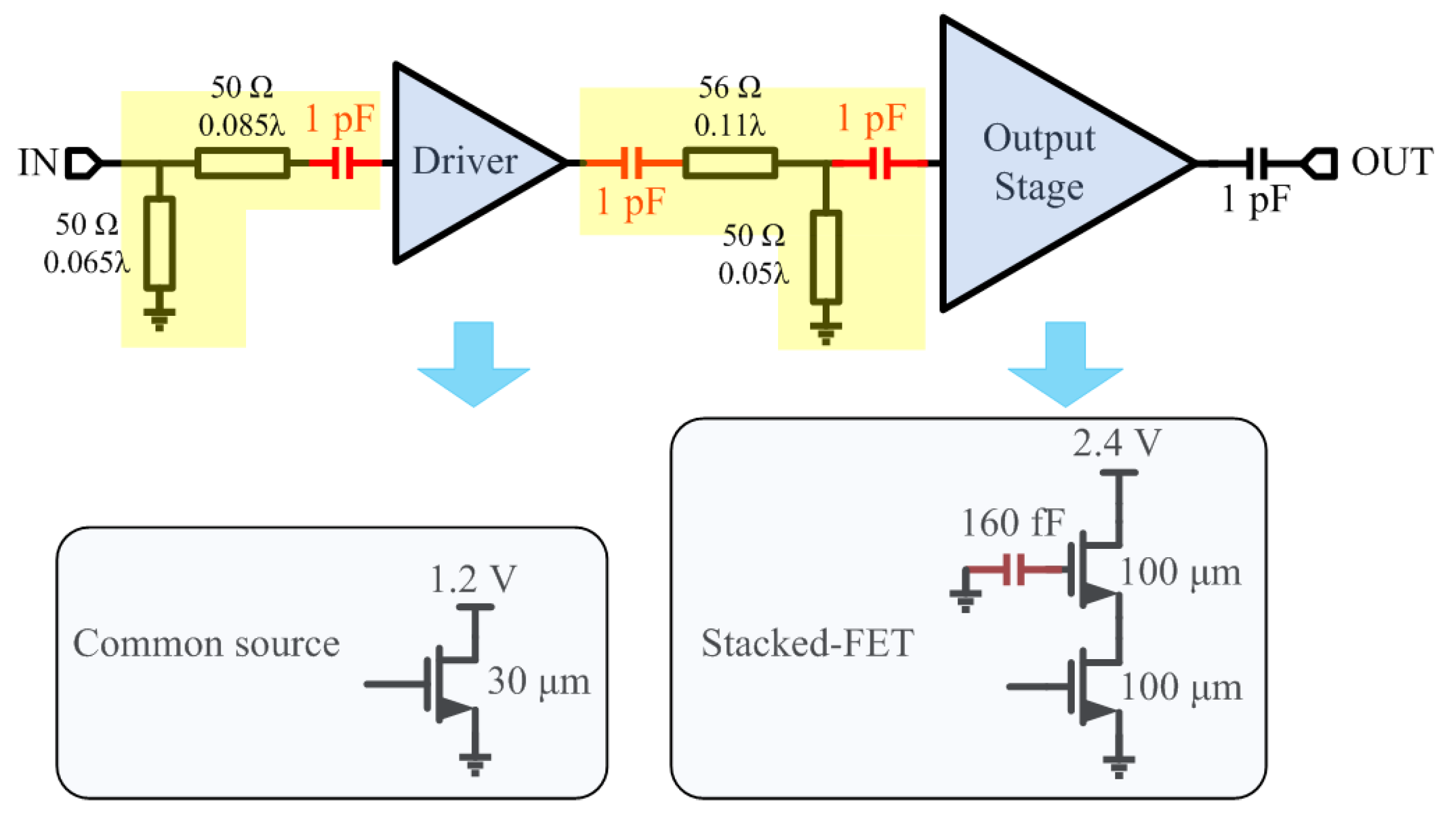
On the basis of the CPW matching networks with series-connected DC-blocking capacitors, we implement a 28 GHz stacked-FET PA, as is shown in Figure 5. The PA consists of a drive stage and an output stage. The stacked-FET architecture is adopted in the output stage to boost the output power. Since the performance of the stacked-FET architecture is mainly tuned by the capacitor connected with the gate of stacked MOSFET, a smaller die area can be achieved compared to the power combination technique. Common source structure is elected in the drive stage to provide high gain. All MOSFETs are biased at class-A mode to obtain highest linearity, which is extremely important for 5G PA.
One series-connected DC-blocking capacitor is used in the input CPW matching network to achieve isolation between the gate voltage in drive stage and the ground. The direct short path to the ground in the input matching network provides an ESD protection for the PA. Two series-connected DC-blocking capacitors are added in the inter-stage CPW matching network to isolate the drain voltage of the drive stage and the gate voltage of the output stage.
In this paper, the load-line method is used to calculate optimum load impedance (Ropt) and saturated output power (Psat) of a single MOSFET. Generally, a large MOSFET can provide a high Psat and a small Ropt. The optimum load impedance is nRopt for an n-stacked-FET topology according to the theory proposed in [22], and the total output power of an n-stacked-FET topology is approximately proportional to the number of stacked MOSFETs, n. In this work, size of MOSFET in output stage is optimized as 100 μm, and the output matching network is not needed.
In the stacked-FET PA, the swing voltage is equally distributed over the drain and source of each MOSFET with an optimum capacitor connected to the gate of stacked MOSFET, and a 160 fF capacitor is chosen for this purpose.

3. Measurements and Results

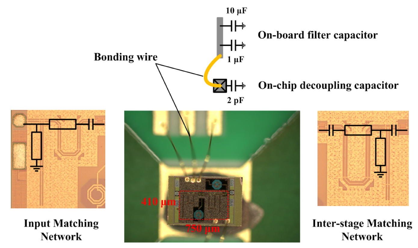
The PA is prototyped in 90 nm SOI CMOS technology, and the chip microphotograph is shown in Figure 6. The developed PA occupies a core area of 0.75 × 0.41 mm2. A printed circuit board (PCB) is designed and fabricated for on-chip measurements. All DC bias voltages are added through bonding wires. A 1 μF filter capacitor and a 10 μF filter capacitor are used in parallel near each pad on a PCB to suppress the low-frequency oscillation. A 2 pF MIM capacitor is added to each pad to minimize the influence of bonding wires. Infinity ground-signal-ground (GSG) microprobes were used for on-chip measurements, and the PA can work stably during measurement.
The small-signal measurements were conducted using an Agilent E5247A67-GHz network analyzer. The measured and simulated results are shown in Figure 7a. The input port of the circuit was designed to matching with 50 Ω at 26 GHz. The −3 dB bandwidth is about 6.3 GHz from 22.9 GHz to 29.2 GH. A peak gain of 13.7 dB is measured at 25.6 GHz, which is 2.7 dB lower than the simulated result. The S11 is lower than –10 dB from 24.6 GHz to 28.8 GHz with S22 around −5 dB without output matching network. Measured S12 of the PA across the 20–30 GHz band is lower than −35 dB, which indicates a high level of reverse isolation. The measured results demonstrate that CPW matching networks featuring high prediction accuracy are achieved with the implementation of the series-connected DC-blocking capacitors.
The large-signal measurements were also performed. Figure 7b shows the measured and simulated output power, power gain, and power added efficiency (PAE). The PA can produce 14.4 dBm saturated output power with 10.8 dBm O P 1 d B at 25.6 GHz. The maximum PAE of the proposed PA is 25%. The measured saturated output power is 1 dB higher than the simulated result, leading to a higher peak PAE.
In order to test the linearity of the PA, the adjacent channel power ratio (ACPR) and the error vector magnitude (EVM) were also carefully measured using an SMW200A vector signal generator and the FSW signal and spectrum analyzer of Rohde & Schwarz, as is shown in Figure 8. A 250 MHz-wide 64-QAM signal is generated for the measurements. The insertion loss of probes, cables, and connectors is calibrated before the measurement.
The measured EVM at 24/25.6/28 GHz with the output power swept are shown in Figure 9a. In Figure 9b, the measured EVM at 9.6 dB PBO is about 2 dB lower than the results at 6 dB PBO at 24 GHz and 25.6 GHz. The measured EVM is slightly low at 28 GHz. The PA achieves +7.87/+9.16/+10.7 dBm measured output power and 6.21%/8.11%/10.17% PAE at −25 dBc EVM as Figure 9c illustrated. The broadband and linear performance of the fabricated PA in high speed dynamic operation is verified by these measurements, which is very important for 5G applications.
A comprehensive summary of the performance of the developed PA and comparisons with other published state-of-the-art works are shown in Table 1. The PA fabricated in 90 nm SOI CMOS technology demonstrates a high linearity and a relatively compact size. The small signal gain and the saturated output power are comparable with [5,6,13]. The peak PAE of the developed PA is partly limited by the adopted class-A operation mode.
The CPW technique is widely used in mm-Wave integrated circuits. The CPW matching networks with series-connected DC-blocking capacitors are less sensitive to the capacitance. Small capacitors featuring high-Q are well suited for this type of topology, and low-loss CPW matching networks with high prediction accuracy can be achieved, which is of great significance for the mm-Wave circuits based on the CPW technique.

4. Conclusions

In this paper, the influence of the DC-blocking capacitors leveraged in CPW matching networks is studied, which is very important for the implementation of CPW technique in mm-Wave chips. CPW matching networks with series-connected DC-blocking capacitors are less sensitive to capacitance and are adopted in a 28 GHz PA fabricated in 90 nm SOI CMOS technology. The developed low-cost PA based on CPW technique with a core area of 0.31 mm2 achieves high linearity, which provides a great potential for 5G applications.

Author Contributions

Conceptualization, Q.X.; methodology, D.L.; software, J.H.; validation, J.L.; resources, H.C.; writing—review and editing, B.S.; project administration, H.L. All authors have read and agreed to the published version of the manuscript.

Funding

This work was supported by the National Key Research and Development Program of China under Grant No. 2016YFA0202304 and 2016YFA0201903, General Program of National Natural Science Foundation of China under Grant No.61674168 and 61504165, as well as the Opening Project of Key Laboratory of Microelectronics Devices and Integrated Technology, Institute of Microelectronics, Chinese Academy of Sciences.

Acknowledgments

The authors would like to thank Rohde & Schwarz for the measurement support.

Conflicts of Interest

The authors declare no conflict of interest. The funders had no role in the design of the study; in the collection, analyses, or interpretation of data; in the writing of the manuscript, or in the decision to publish the results.

References

  1. Kim, H.T.; Park, B.S.; Song, S.S.; Moon, T.S.; Kim, S.H.; Kim, J.M.; Chang, J.Y.; Ho, Y.C. A 28-GHz CMOS direct conversion transceiver with packaged 2 × 4 antenna array for 5G cellular system. IEEE J. Solid-State Circuits 2018, 53, 1245–1259. [Google Scholar] [CrossRef]
  2. Kibaroglu, K.; Sayginer, M.; Phelps, T.; Rebeiz, G.M. A 64-element 28-GHz phased-array transceiver with 52-dBm EIRP and 8-12-Gb/s 5G link at 300 meters without any calibration. IEEE Trans. Microw. Theory Tech. 2018, 66, 5796–5811. [Google Scholar] [CrossRef]
  3. Pang, J.; Wu, R.; Wang, Y.; Dome, M.; Kato, H.; Huang, H.; Narayanan, A.T.; Liu, H.; Liu, B.; Nakamura, T.; et al. A 28-GHz CMOS phased-array transceiver based on LO phase-shifting architecture with gain invariant phase tuning for 5G new radio. IEEE J. Solid-State Circuits 2019, 54, 1228–1242. [Google Scholar] [CrossRef]
  4. Enabling Mobile Augmented and Virtual Reality with 5G Networks. Available online: http://about.att.com/innovationblog/foundry_ar_vr (accessed on 27 February 2017).
  5. Hu, S.; Wang, F.; Wang, H. A 28-/37-/39-GHz linear Doherty power amplifier in silicon for 5G applications. IEEE J. Solid-State Circuits 2019, 54, 1586–1599. [Google Scholar] [CrossRef]
  6. Shakib, S.; Park, H.C.; Dunworth, J.; Aparin, V.; Entesari, K. A highly efficient and linear power amplifier for 28-GHz 5G phased array radios in 28-nm CMOS. IEEE J. Solid-State Circuits 2016, 51, 3020–3036. [Google Scholar] [CrossRef]
  7. Nikandish, G.; Staszewski, R.B.; Zhu, A. Breaking the bandwidth limit: A review of broadband Doherty power amplifier design for 5G. IEEE Microw. Mag. 2020, 21, 57–75. [Google Scholar] [CrossRef] [Green Version]
  8. Chou, C.F.; Wu, C.W.; Hsiao, Y.H.; Wu, Y.C.; Lin, Y.H.; Wang, H. A 60-GHz 20.6-dBm Symmetric Radial Combining Wideband Power Amplifier with 20.3% Peak PAE and 20-dB Gain in 90-nm CMOS. In Proceedings of the 2016 IEEE MTT-S International Microwave Symposium (IMS), San Francisco, CA, USA, 22–27 May 2016. [Google Scholar]
  9. Huang, W.C.; Lin, J.L.; Lin, Y.H.; Wang, H. A K-band Power Amplifier with 26-dBm Output Power and 34% PAE with Novel Inductance-based Neutralization in 90-nm CMOS. In Proceedings of the 2018 IEEE Radio Frequency Integrated Circuits Symposium (RFIC), Philadelphia, PA, USA, 10–12 June 2018; pp. 228–231. [Google Scholar]
  10. Helmi, S.R.; Chen, J.H.; Mohammadi, S. High-efficiency microwave and mm-Wave stacked cell CMOS SOI power amplifiers. IEEE Trans. Microw. Theory Tech. 2016, 64, 2025–2038. [Google Scholar] [CrossRef]
  11. Fang, K.; Buckwalter, J.F. Efficient linear millimetre-wave distributed transceivers in CMOS SOI. IEEE Trans. Microw. Theory Tech. 2019, 67, 295–307. [Google Scholar] [CrossRef]
  12. Cheung, T.S.; Long, J.R.; Vaed, K.; Volant, R.; Chinthakindi, A.; Schnabel, C.M.; Florkey, J.; Stein, K. On-chip interconnect for mm-Wave applications using all-copper technology and wavelength reduction. ISSCC Dig. Tech. Papers 2003. [CrossRef]
  13. Komijani, A.; Natarajan, A.; Hajimiri, A. A 24-GHz, +14.5-dBm fully integrated power amplifier in 0.18-μm CMOS. IEEE J. Solid-State Circuits 2005, 40, 1901–1908. [Google Scholar]
  14. Siligaris, A.; Mounet, C.; Reig, B.; Vincent, P. CPW discontinuities modelling for circuit design up to 110 GHz in SOI CMOS technology. In Proceedings of the 2007 IEEE Radio Frequency Integrated Circuits (RFIC) Symposium, Honolulu, HI, USA, 3–5 June 2007; pp. 295–298. [Google Scholar]
  15. Haroun, I.; Wight, J.; Plett, C.; Fathy, A.; Hsu, Y.C. A V-band 90-nm CMOS low-noise amplifier with modified CPW transmission lines for UWB systems. In Proceedings of the Topical Meeting on Silicon Monolithic Integrated Circuits in RF Systems, New Orleans, LA, USA, 11–13 January 2010; pp. 160–163. [Google Scholar]
  16. Lee, S.Y.; Cheng, P.H.; Tsou, C.F.; Lin, C.C.; Shieh, G.S. A 2.4 GHz ISM band OOK transceiver with high energy efficiency for biomedical implantable applications. IEEE Trans. Biomed. Circuits Syst. 2020, 14, 113–124. [Google Scholar] [CrossRef] [PubMed]
  17. Choe, Y.J.; Nam, H.; Park, J.D. A compact 5 GHz power amplifier using a spiral transformer for enhanced power supply rejection in 180-nm CMOS technology. Electronics 2019, 8, 1043. [Google Scholar] [CrossRef] [Green Version]
  18. Shu, R.; Subramanian, V.; Hamidian, A.; Malignaggi, A.; Boeck, G. Characterization of LC-tank circuits for mm-Wave applications in 90 nm CMOS. In Proceedings of the 2011 Semiconductor Conference Dresden, Dresden, Germany, 27–28 September 2011. [Google Scholar]
  19. Korndorfer, F.; Muhlhaus, V. Lumped modelling of integrated MIM capacitors for RF applications. In Proceedings of the 2016 88th ARFTG Microwave Measurement Conference (ARFTG), Austin, TX, USA, 8–9 December 2016. [Google Scholar]
  20. Beeresha, R.S.; Khan, A.M.; Manjunath Reddy, H.V. Design and EM-simulation of MIM capacitor. In Proceedings of the 2017 International Conference on Energy, Communication, Data Analytics and Soft Computing (ICECDS), Chennai, India, 1–2 August 2017; pp. 1644–1649. [Google Scholar]
  21. Rohani, N.; Zhang, J.; Lee, J.; Bai, J. A 28-nm CMOS 76-81-GHz power amplifier for automotive radar applications. In Proceedings of the 2017 IEEE 17th Topical Meeting on Silicon Monolithic Integrated Circuits in RF Systems (SiRF), Phoenix, AZ, USA, 15–18 January 2017; pp. 85–87. [Google Scholar]
  22. Dabag, H.T.; Hanafi, B.; Golcuk, F.; Agah, A.; Buckwalter, J.F.; Asbeck, P.M. Analysis and design of stacked-FET millimeter-wave power amplifiers. IEEE Trans. Microw. Theory Tech. 2013, 61, 1543–1556. [Google Scholar] [CrossRef]
Figure 1. (a) Spectra for 5th generation (5G) applications proposed by different regions in the world, (b) an example of a transmitter frontend for 5G phased array.
Electronics 09 00617 g001
Figure 2. (a) The cross-section of the 90 nm SOI-CMOS technology, a 200 μm, 50 Ω microstrip (MST) line, a 200 μm, 50 Ω coplanar waveguide (CPW) line, and the simulation setup, (b) the simulated imaginary part of the impedance seen from port1, (c) simulated attenuation of CPW line and MST line.
Electronics 09 00617 g002
Figure 3. (a) Smith chart trajectories for input matching of the PA, (b) CPW matching network with series-connected DC-blocking capacitor, (c) CPW matching-network with parallel-connected DC-blocking capacitor.
Electronics 09 00617 g003
Figure 4. (a) Simulated S21 of the topology with series-connected DC-blocking capacitor, (b) simulated S21 of the topology with parallel-connected DC-blocking capacitor, (c) simulated S11 of the topology with series-connected DC-blocking capacitor, (d) simulated S11 of the topology with parallel-connected DC-blocking capacitor, (e) simulated S22 of the topology with series-connected DC-blocking capacitor, (f) simulated S22 of the topology with parallel-connected DC-blocking capacitor.
Electronics 09 00617 g004
Figure 5. Schematic of the proposed PA. Series-connected DC-blocking capacitors are utilized in the CPW matching networks.
Electronics 09 00617 g005
Figure 6. Chip microphotograph of the developed PA with on-chip decoupling capacitor and on-board filter capacitors.
Electronics 09 00617 g006
Figure 7. (a) Small-signal measurements and simulations of the PA, (b) large-signal measurements and simulations of the PA.
Electronics 09 00617 g007
Figure 8. The measurement setup for adjacent channel power ratio (ACPR) and error vector magnitude (EVM) and the measured results at 25.6 GHz operation frequency and 9.6 dB power back-off (PBO).
Electronics 09 00617 g008
Figure 9. (a) EVM versus average 64-QAM output power for 250 MHz BWsig at 24/25.6/28 GHz, (b) EVM versus carrier frequency at 6/9.6 dB PBO, (c) average output power and corresponding PAE versus carrier frequency at fixed EVM of −25 dBc.
Electronics 09 00617 g009
Table 1. Performance summary and comparison.
This WorkJSSC’ 19 [5]JSSC’ 16 [6]RFIC’ 18 [9]JSSC’ 05 [13]
Technology90 nm SOI CMOS130 nm SiGe28 nm CMOS90 nm CMOS0.18 μm CMOS
Matching networkCPW lineTransformer & capacitorTransformer & capacitorTransformer & capacitorSlow-wave CPW line
Gain (dB)13.718.215.716.37
−3 dB BW (GHz)6.316.43.85-3.1
Psat (dBm)14.416.8142614.5
Peak PAE (%)2520.335.534.16.5
Modulation64-QAM 1.5 Gb/s64-QAM 6 Gb/s64-QAM OFDM 1.5 Gb/s256-QAM PRBS15 1.6 Gb/s-
EVM @ 28 GHz, (dBc)−29.4 dBc @ 9.6 dB PBO−26.6 dBc @ 9.6 dB PBO−25 dBc @ 9.6 dB PBO 1<−32 dBc 2-
Area (mm2)0.311.760.160.401 31.26 3
1 Measured result at 30 GHz, 2 Calculated from measured results, 3 Pads are included.