Article

Understanding of Polarization-Induced Threshold Voltage Shift in Ferroelectric-Gated Field Effect Transistor for Neuromorphic Applications

Department of Electrical and Computer Engineering, Sungkyunkwan University, Suwon 16419, Korea
*
Author to whom correspondence should be addressed.
Electronics 2020, 9(5), 704; https://doi.org/10.3390/electronics9050704
Submission received: 27 March 2020 / Revised: 24 April 2020 / Accepted: 25 April 2020 / Published: 25 April 2020
(This article belongs to the Special Issue Steep-Switching Devices)

Abstract

:
A ferroelectric-gated fin-shaped field effect transistor (Fe-FinFET) is fabricated by connecting a Pb(Zr0.2Ti0.8)O3-based ferroelectric capacitor into the gate electrode of FinFET. The ferroelectric capacitor shows coercive voltages of approximately −1.5 V and 2.25 V. The polarization-induced threshold voltage shift in the Fe-FinFET is investigated by regulating the gate voltage sweep range. When the maximum positive gate to source voltage is varied from 4 V to 2 V with a fixed starting negative gate to source voltage, the threshold voltage during the backward sweep is increased from approximately −0.60 V to 1.04 V. In the case of starting negative gate to source voltage variation from −4 V to −0.5 V with a fixed maximum positive gate to source voltage of 4 V, the threshold voltage during the forward sweep is decreased from 1.66 V to 0.87 V. Those results can be elucidated with polarization domain states. Lastly, it is observed that the threshold voltage is mostly increased/decreased when the positive/negative gate voltage sweep range is smaller/larger than the positive/negative coercive voltage, respectively.

1. Introduction

Following Moore’s law, the footprint of a transistor in as integrated circuit has been aggressively scaled down, resulting in improved performance/power consumption/integrity of integrated chips (ICs). In order to keep the Moore’s law alive, various steep switching devices featuring sub-60 mV/decade subthreshold slope (SS) have been proposed, resulting in overcoming the lower limit of SS (i.e., 60 mV/decade at 300 K), a.k.a., Boltzmann tyranny: tunnel field-effect transistor (TFET) [1], phase-transition FET [2,3], feedback FET [4,5], and negative capacitance FET (NCFET) [6]. Despite these advancements in transistors (especially for low-power applications), semiconductor societies have difficulties in realizing the Internet of Things (IoT) owing to the processing of enormous amounts of data [7,8]. Conventionally, von-Neumann-architecture-based computing systems have been used for processing large quantities of data, but such architectures encounter limitations in the realm of big data [9]. In recent years, the mimicking of biological brain synapses for neuromorphic systems has been widely investigated with the idea that these systems can process tremendous amounts of data at a faster transfer rate [10,11,12,13]. Non-volatile memory devices have been researched as synapse devices for the neuromorphic system, such as phase-change memory [14,15], resistive random-access memory [16], conductive-bridge random-access memory [17], and ferroelectric-gated FET (FeFET) [18]. Among these candidates, FeFET has been highlighted because FeFET can be fabricated by simply inserting a ferroelectric layer into the gate stack of a conventional MOSFET [19,20,21]. Having the same footprint as the conventional FETs, the FeFET can have non-volatile memory characteristics. FeFETs can mimic biological synapse characteristics as the ferroelectric domains are gradually switched by continuously applying a voltage, which leads to the threshold voltage shift and manipulation of the conductivity of FeFET [22,23,24].
Recently, ways to take advantage of hysteresis of FeFET for neuromorphic systems have been demonstrated (i.e. FeFET-based spiking neural networks (SNNs) [25,26] and oscillators [27]). Moreover, thanks to the CMOS-compatible device structure, an integrated ferroelectric-gated fin-shaped FET for neuromorphic applications has been introduced [28]. It has been also demonstrated that FeFETs can be utilized as multi-bit synapse devices by adjusting the number of ferroelectric domains [29]. From this point of view, the impact of domain switching on the operation of FeFET needs to be investigated to comprehend more deeply the operation of FeFET-based synapse devices. However, the experimental results have placed emphasis on the characteristics of neuromorphic synapse devices. Investigations on the polarization-induced threshold voltage shift are still lacking. Specifically, the effect of polarization switching from individual domains needed to be revealed. Therefore, in this study, the impacts of polarization behavior on the characteristics of a ferroelectric-gated fin-shaped FET (Fe-FinFET) are experimentally investigated by means of analyzing the input transfer characteristics. The Fe-FinFET used in this experiment was fabricated by connecting a Pb(Zr0.2Ti0.8)O3 (PZT)-based ferroelectric capacitor to the gate region of a baseline FinFET. The threshold voltage in the backward sweep (Vth_backward) of the Fe-FinFET increases from −0.60 V to 1.04 V, when the maximum positive gate-to-source voltage (VGS_positive) with a negative gate-to-source voltage (VGS_negative) of −4V is decreased from 4 V to 1 V. On the other hand, when VGS_negative is varied from −4 V to 0 V with a fixed VGS_positive of 4 V, the threshold voltage in the forward sweep (Vth_forward) decreases from 1.67 V to 0.87 V. Those results are elucidated with polarization switching and coercive voltage in ferroelectric material.

2. Fabrication and Measurement

In this work, n-type enhancement mode FinFET is utilized as a baseline FET. The schematics of the Fe-FinFET are illustrated in Figure 1. The baseline FinFET has 80 nm, 30 nm, 40 nm, 5, 200 nm, and 1.4 nm channel length, fin width, fin height, number of fins, fin pitch, and equivalent oxide thickness, respectively. The fabrication process of the PZT ferroelectric capacitor used in this work is as follows: (i) a NdScO3 substrate was prepared and (ii) a 20 nm-thick La0.7Sr0.3MnO3 was deposited as the bottom electrode. Subsequently, (iii) a 60nm-thick Pb(Zr0.2Ti0.8)O3 (PZT) ferroelectric film was deposited using a pulsed laser deposition technique. Lastly, (iv) 60 nm-thick Au/Ti/Au top electrodes were deposited and patterned. The flow of the aforementioned fabrication process is illustrated in Figure 2b. The Fe-FinFET was implemented by physically linking the PZT-based ferroelectric capacitor to the gate region of baseline FinFET with gold wire. Each measurement was done using the Keithley 4200A-SCS semiconductor parameter analyzer at 300 K. For the input transfer curve measurement, forward and backward gate voltage sweep are done in sequence.
In the measurement, the gate-to-source voltage is applied to the device from VGS_negative to VGS_positive (i.e., forward sweep), then the gate-to-source voltage is applied to the device from VGS_positive to VGS_negative (i.e., backward sweep). In this work, the ranges of the gate voltage sweep are varied in two opposite ways: (1) VGS_positive decreases from 4 V to 1 V with the fixed VGS_negative of −4 V. (2) VGS_negative increases from −4 V to 0 V with the fixed VGS_positive of 4 V. Note that Vth_forward and Vth_backward were extracted using the constant current method at 1.375 × 10⁻⁷ A (i.e., 10−7 A × (2Hfin + Wfin)/Lfin). The hysteresis width was calculated by subtracting Vth_backward from Vth_forward.

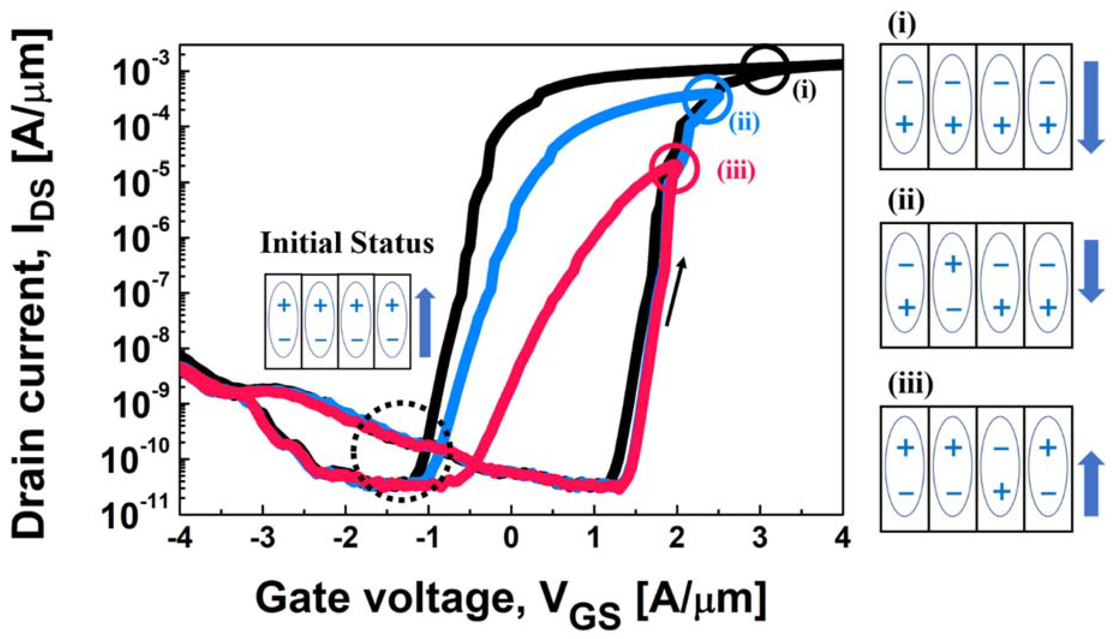
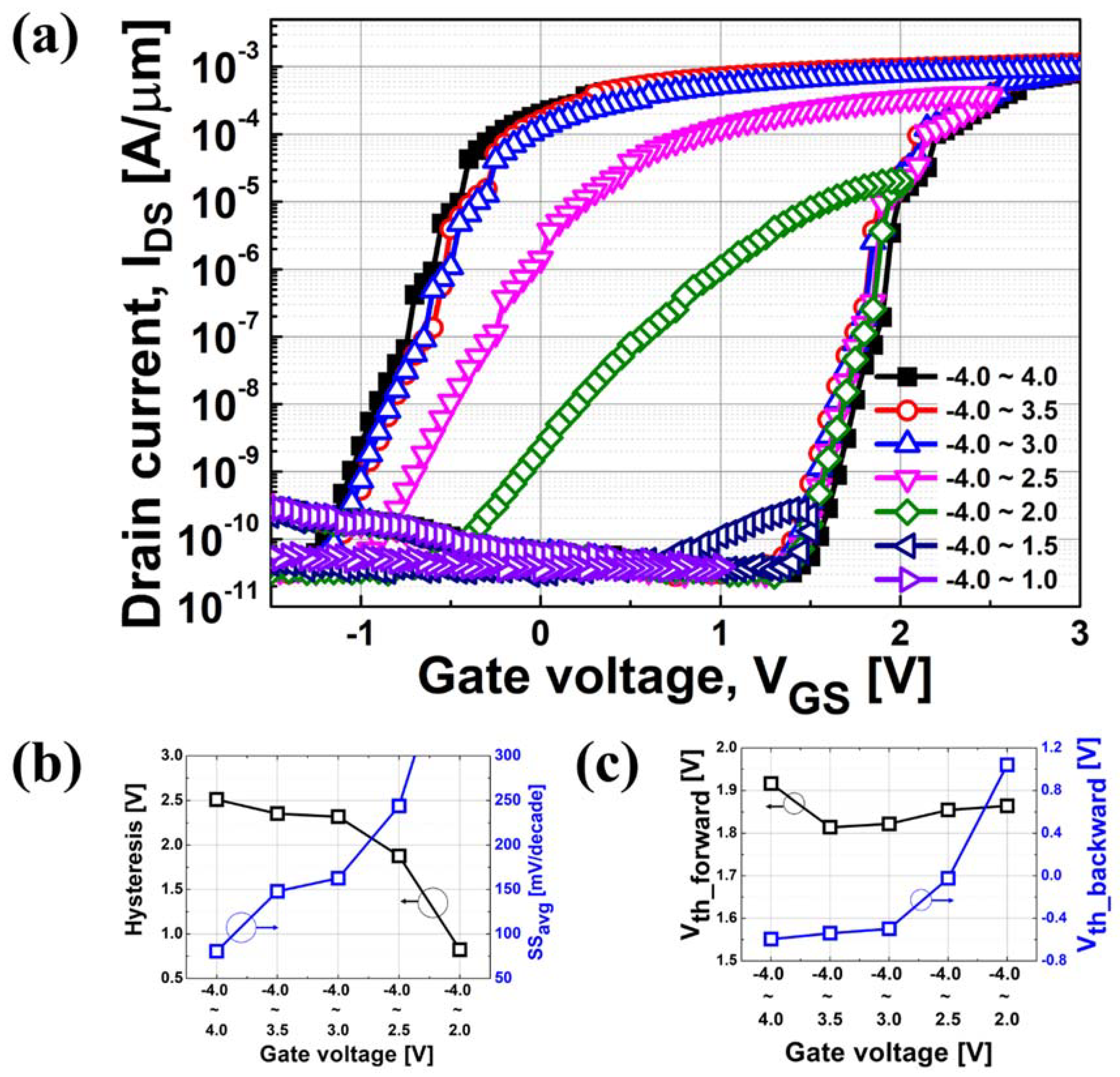
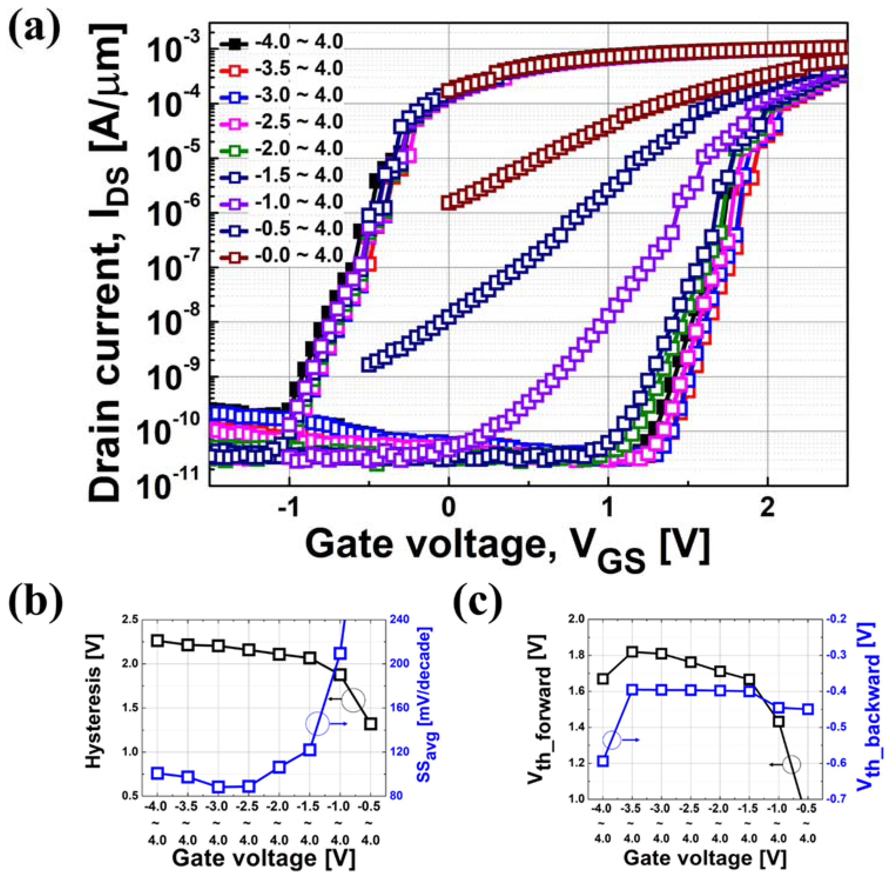
3. Results and Discussion

The ferroelectric layer with a single domain has only two polarization states (i.e., upward or downward direction). When a voltage higher than the coercive voltage is applied, a polarization state can be inverted to the other state. However, most of practical ferroelectric layers have a multi-domain structure [30]. Each domain in the ferroelectric layer has its own coercive voltage because it has more or less doping concentration and grain size than the other domains. As a result, an externally applied voltage can switch the polarization direction of only those domains which have a lower coercive voltage than the applied voltage [31,32,33,34,35]. This partial polarization switching can gradually change the conductivity of FeFETs for neuromorphic applications [36]. In order to investigate the partial polarization switching, we have fabricated a ferroelectric capacitor, and its measured capacitance (C)−voltage (V) is drawn in Figure 2a. The positive and negative coercive voltage of the ferroelectric capacitor are ~2.25 and ~−1.5 V, respectively. Compared with previous results which show one sharp peak [22], the two peaks at the negative coercive voltage would have originated from aging effect. Although it casts doubt on the ferroelectricity, this device still shows the properties of a ferroelectric layer [see Figure S1 in Supplementary Information]. Figure 3 illustrates the measured input transfer curves of FeFET for various VGS_positive with the same VGS_negative. For all cases [i.e., (i), (ii), and (iii)], the VGS_negative (which is higher than the negative coercive voltage of ferroelectric capacitor for the FeFET) is identical, so that the initial polarization state is identical (i.e., the initial state is aligned upward). As a result, the Vth_forward of the three cases are almost identical. In the case of (i), the VGS_positive induces complete polarization switching, and, thereby, all the domains in the ferroelectric layer are switched to the downward direction. This should result in the Vth_backward being lower than the Vth_forward. The reason for this observation comes from the fact that the downward polarization (in addition to the vertical electrical field from the gate electrode) contributes to the accumulation of electrons when forming a channel. However, in the case of (ii) and (iii), the VGS_positive is not high enough to switch every domain, which results in partial polarization switching (i.e., partially downward). Therefore, the Vth_backward for case (ii) and (iii) is higher than the value for case (i).
In order to analyze the impact of partial polarization switching on the operation of synapse devices, a FeFET was fabricated and then measured with different VGS_positive values (i.e., from 4 to 1 V) for a fixed VGS_negative (i.e., −4 V) [see Figure 4a]. For 3–4 V of the VGS_positive, the situations are corresponding to the case of (i) shown in Figure 3 (i.e., complete polarization switching). Although the VGS_positive values are different (i.e., 3 V or 4 V), the Vth_backward values are similar to each other. In reality, the Vth_backward values for the positive gate voltages of 4, 3.5, and 3 V are approximately −0.60, −0.54, and −0.49 V, respectively. These measurement results indicate that there are few domains which have coercive voltages between 3 and 4 V in the ferroelectric layer. Conversely, for the case of the VGS_positive from 2.5 V to 2 V (which is comparable to the positive coercive voltage of ~2.25 V), the Vth_backward increases from approximately −0.02 to 1.04 V. This situation corresponds to either case (ii) or (iii), as shown in Figure 3. This represents the partial polarization switching occurring in the ferroelectric layer, resulting in the threshold voltage shift. In the case of VGS_positive from 2 V to 1 V, the Fe-FinFET is not turned on due to the lack of gate voltage sweep range. Regardless of the VGS_positive in all the measurements, the Vth_forward values are almost identical when the device is turned on, because the initial polarization states are the same as described above. The Vth_forward and Vth_backward variation is characterized as a function of VGS_positive [see Figure 4c]. Figure 4b shows the hysteresis and subthreshold slope during backward voltage sweep (SSavg_backward) vs. gate voltage. As the hysteresis is decreased from ~2.51 to ~0.82 V due to the Vth_backward shift, the SSavg_backward increases from ~80 to ~462 mV/decade. This can be understood and explained using SS and load-line analysis in FeFETs [6,37,38,39]. A detailed analysis is described in the Supplementary Information (see the Figure S2 in the Supplementary Materials].
Figure 5a shows the measured input transfer curves for various VGS_negative (i.e., from −4 to 0 V) with a fixed VGS_positive of 4 V. Contrary to the previous measurements adjusting VGS_positive, the Vth_negative is maintained regardless of the gate voltage sweep range. The reason for the observation shown in Figure 5 is that the polarization states during the backward sweeps are identical owing to the complete polarization switching from the fixed VGS_positive, whereas the Vth_forward decreases as the VGS_negative increases from −4 to 0 V. When the VGS_negative is changed from −4 to −1.5 V, the Vth_forward is almost unvaried within the range of ~1.82 to ~1.67 V [see Figure 5c]. This situation corresponds to the case of manipulating VGS_positive from 4 to 3 V. The unvaried Vth_forward means that there are few domains having a negative coercive voltage that is smaller than −3 V. The Vth_forward starts to further decrease as the VGS_negative becomes larger than −1.5 V (i.e., a similar value to the positive coercive voltage of approximately −1.5 V). The Vth_forward for the VGS_negative of −1 and −0.5 V are ~1.43 and ~0.87 V, respectively. The decrease in Vth_forward originates from the polarization state after the measurement immediately before (i.e., the case of VGS_negative of −1.5 V). After this measurement, the polarization states are not fully arranged to the upward direction due to some domains which have a negative coercive voltage smaller than −1.5 V. As a result, electrons can be assembled to form a channel at a gate voltage lower than the previously measured one. Similarly, in the case of VGS_negative of 0 V, the Vth_forward is decreased, but the current level becomes so high that the exact Vth_forward cannot be extracted using the constant current method at 1.375 × 10⁻⁷ A. These Vth_forward and Vth_backward variations are plotted in Figure 5c. Figure 5b shows the well-known relationship between the hysteresis (from ~2.26 to ~1.32 V) and SSavg (from ~101 to ~416 mV/decade).
From all the measurement data shown above, various parameters and characteristics for neuromorphic applications (e.g., pulse amplitude used for the function of “firing”) can be acquired. This is because VGS_positive and VGS_negative are equivalent to the amplitude of pulse measurement, in terms of electrical effects, which is the usual method for investigating the characteristics of neuromorphic applications. To be specific, it can be deduced that, if this device is used as a synapse device, the maximum pulse amplitude should not exceed 3 V because it will not affect any polarization state [see Figure 4a]. It can also be found that the threshold voltage shift is originated from the ferroelectricity. This means that if the device shows the characteristics of FeFET (even though the fabrication process or materials are changed), the contents (i.e., the trend shown in Figure 4 and Figure 5) in this work should be applicable. Furthermore, this externally connected device structure is useful when various properties of capacitors need to be investigated, because the capacitor can be simply replaced with other ones. For example, in an externally connected device structure, a sufficiently scaled-down ferroelectric capacitor, which has a few domains, can be used for investigating multi-bit neuromorphic systems without scaling down the baseline FET. On the other hand, in an integrated FeFET structure, the ferroelectric capacitor and baseline FET must be scaled down together to realize a few domains [23,24]. Likewise, using the externally connected device structure, we expect that the polarization-induced threshold voltage shift in FeFET will facilitate decisions about various parameters in neuromorphic applications.

4. Conclusions

The threshold voltage shift characteristics of the Fe-FinFET with a PZT-based ferroelectric capacitor were studied to understand the impact of polarization state on the device operation. The PZT-based ferroelectric capacitor had approximately 2.25 V and −1.5 V of the positive coercive voltage and negative coercive voltage, respectively. The Fe-FinFET was measured with various gate-to-source voltage sweep ranges. Because of the partial polarization switching (i.e., partially downward), the Vth_backward was increased from −0.60 to 1.04 V when the VGS_positive was decreased from 4 to 2 V for the same VGS_negative of −4 V. When the VGS_positive was adjusted to a value similar to the positive coercive voltage (i.e., 2.5 and 2 V), the Vth_backward was increased to −0.02 and 1.04 V, respectively. When the VGS_negative was regulated from −4 to −0.5 V for the same VGS_positive of 4 V, the Vth_forward was decreased from ~1.67 to ~0.87 V. Similarly, the Vth_forward was decreased to ~1.43 and ~0.87 V when the VGS_negative was changed to a value similar to the negative coercive voltage (i.e., −1 and −0.5 V), respectively. From this research, it was proposed that the externally connected FeFET can contribute to the understanding of the operation of FeFET-based synapse devices in a different way, with the investigation of integrated FeFET-based synapse devices. For multi-bit neuromorphic applications, investigation of the synaptic characteristics of FeFET with sufficiently tiny ferroelectric capacitors needs to be implemented.

Supplementary Materials

The following are available online at https://www.mdpi.com/2079-9292/9/5/704/s1, Figure S1: The charge vs. voltage plot of the Pb(Zr0.2Ti0.8)O3-based ferroelectric capacitor, Figure S2: (a) Capacitive network of ferroelectric-gated FET; (b) load-line analysis of ferroelectric-gated FET.

Author Contributions

S.M. and J.S. equally contributed to this work. Conceptualization, S.M. and J.S.; methodology, S.M. and J.S.; validation, S.M. and J.S.; formal analysis, S.M. and J.S.; investigation, S.M. and J.S.; resources, S.M. and J.S.; data curation, S.M. and J.S.; writing—original draft preparation, S.M. and J.S.; writing—review and editing, C.S.; visualization, S.M. and J.S.; supervision, C.S.; project administration, C.S.; funding acquisition, C.S. All authors have read and agreed to the published version of the manuscript.

Funding

This work was supported by the National Research Foundation of Korea (NRF) through a grant funded by the Korean Government (MSIP) (No. 2020R1A2C1009063).

Conflicts of Interest

The authors declare no conflicts of interest.

References

  1. Choi, W.Y.; Park, B.G.; Lee, J.D.; Liu, T.J.K. Tunneling Field-Effect Transistors (TFETs) With Subthreshold Swing (SS) Less Than 60 mV/dec. IEEE Electron Device Lett. 2007, 28, 743–745. [Google Scholar] [CrossRef]
  2. Shin, J.; Ko, E.; Shin, C. Super steep-switching (S ≈ 2 mV/decade) phase-FinFET with Pb(Zr0.52Ti0.48)O3 threshold switching device. Appl. Phys. Lett. 2018, 113, 102–104. [Google Scholar] [CrossRef]
  3. Shukla, N.; Thathachary, A.V.; Agrawal, A.; Paik, H.; Aziz, A.; Schlom, D.G.; Gupta, S.K.; Engel-Herbert, R.; Datta, S. A steep-slope transistor based on abrupt electronic phase transition. Nat. Commun. 2015, 6, 7812. [Google Scholar] [CrossRef] [Green Version]
  4. Lee, C.; Ko, E.; Shin, C. Steep slope silicon-on-insulator feedback field-effect transistor: Design and performance analysis. IEEE Trans. Electron Devices 2018, 66, 286–291. [Google Scholar] [CrossRef]
  5. Kim, M.; Kim, Y.; Lim, D.; Woo, S.; Cho, K.; Kim, S. Steep switching characteristics of single-gated feedback field-effect transistors. Nat. Nanotechnol. 2016, 28, 055205. [Google Scholar] [CrossRef] [PubMed]
  6. Salahuddin, S.; Datta, S. Use of negative capacitance to provide voltage amplification for low power nanoscale devices. Nano Lett. 2008, 8, 405–410. [Google Scholar] [CrossRef] [PubMed]
  7. Yu, S.; Chen, P.-Y. Emerging memory technologies: Recent trends and prospects. IEEE Solid State Circuits Mag. 2016, 8, 43–56. [Google Scholar] [CrossRef]
  8. Wong, H.S.P.; Salahuddin, S. Memory leads the way to better computing. Nat. Nanotechnol. 2015, 10, 191–194. [Google Scholar] [CrossRef] [PubMed] [Green Version]
  9. Li, Y.; Zhong, Y.; Zhang, J.; Xu, L.; Wang, Q.; Sun, H.; Tong, H.; Cheng, X.; Miao, X. tre-Dependent Synaptic Plasticity of a Chalcogenide Electronic Synapse for Neuromorphic Systems. Sci. Rep. 2014, 4, 4906. [Google Scholar] [CrossRef] [PubMed] [Green Version]
  10. Indiveri, G.; Liu, S.C. Memory and Information Processing in Neuromorphic Systems. Proc. IEEE. 2015, 103, 1379–1397. [Google Scholar] [CrossRef] [Green Version]
  11. LeCun, Y.; Bengio, Y.; Hinton, G. Deep learning. Nature 2015, 521, 436–444. [Google Scholar] [CrossRef] [PubMed]
  12. Wang, Z.; Khan, A.I. Ferroelectric Relaxation Oscillators and Spiking Neurons. IEEE J. Explor. Solid State Computat. 2019, 5, 151–157. [Google Scholar] [CrossRef]
  13. Tan, A.J.; Chatterjee, K.; Zhou, J.; Kwon, D.; Liao, Y.-H.; Cheema, S.; Hu, C.; Salahuddin, S. Experimental Demonstration of a Ferroelectric HfO2-based Content Addressable Memory Cell. IEEE Electron Dev. Lett. 2020, 41, 240–243. [Google Scholar] [CrossRef]
  14. Bez, R. Chalcogenide PCM: A memory technology for next decade. IEEE IEDM 2009, 5, 1. [Google Scholar]
  15. Wong, H.-S.P.; Raoux, S.; Kim, S.B.; Liang, J.; Reifenberg, J.P.; Rajendran, B.; Asheghi, M.; Goodson, K.E. Phase Change Memory. Proc. IEEE. 2020, 98, 2201–2227. [Google Scholar] [CrossRef]
  16. Moon, K.; Kwak, M.; Park, J.; Lee, D.; Hwang, H. Improved conductance linearity and conductance ratio of 1T2R synapse device for neuromorphic systems. IEEE Electron Dev. Lett. 2017, 38, 1023–1026. [Google Scholar] [CrossRef]
  17. Kund, M.; Beitel, G.; Pinnow, C.-U.; Rohr, T.; Schumann, J.; Symanczyk, R.; Ufert, K.; Muller, G. Conductive bridging RAM (CBRAM): An emerging non-volatile memory technology scalable to sub 20 nm. IEEE IEDM 2005, 754–757. [Google Scholar] [CrossRef]
  18. Mulaosmanovic, H.; Ocker, J.; Muller, S.; Noack, M.; Muller, J.; Polakowski, P.; Mikolajick, T.; Slesazeck, S. Novel ferroelectric FET based synapse for neuromorphic systems. Symp. VLLSI Tech. Dig. 2017, T176–T177. [Google Scholar] [CrossRef]
  19. Ishiwara, H. Proposal of Adaptive Neuron Circuits with Ferroelectric Analog-Memory Weights. Jpn. J. Appl. Phys. 1993, 32, 442–446. [Google Scholar] [CrossRef]
  20. Jo, J.; Choi, W.Y.; Park, J.-D.; Shim, J.W.; Yu, H.-Y.; Shin, C. Negative capacitance in organic/ferroelectric capacitor to implement steep switching MOS devices. Nano Lett. 2015, 15, 4553–4556. [Google Scholar] [CrossRef]
  21. Ko, E.; Lee, J.W.; Shin, C. Negative Capacitance FinFET with Sub-20-mV/decade Subthreshold Slope and Minimal Hysteresis of 0.48 V. IEEE Electron Device Lett. 2017, 38, 418–421. [Google Scholar] [CrossRef]
  22. Nishitani, Y.; Kaneko, Y.; Ueda, M.; Fujii, E. Three-terminal ferroelectric synapse device with concurrent learning function for artificial neural networks. J. Appl. Phys. 2012, 111, 124108. [Google Scholar] [CrossRef]
  23. Mulaosmanovic, H.; Ocker, J.; Muller, S.; Schroeder, U.; Muller, J.; Polakowski, P.; Flachowsky, S.; Bentum, R.V.; Mikolajick, T.; Slesazeck, S. Switching Kinetics in Nanoscale Hafnium Oxide Based Ferroelectric Field-Effect Transistors. Appl. Mater. Interfaces 2017, 9, 3792–3798. [Google Scholar] [CrossRef]
  24. Oh, S.; Kim, T.; Kwak, M.; Song, J.; Woo, J.; Jeon, S.; Yoo, I.K.; Hwang, H. HfZrOx -based ferroelectric synapse device with 32 levels of conductance states for neuromorphic applications. IEEE Electron Device Lett. 2017, 38, 732–735. [Google Scholar] [CrossRef]
  25. Fang, Y.; Gomez, J.; Wang, Z.; Datta, S.; Khan, A.I.; Raychowdhury, A. Neuro-Mimetic Dynamics of a Ferroelectric FET-Based Spiking Neuron. IEEE Electron Device Lett. 2019, 40, 1213–1216. [Google Scholar] [CrossRef]
  26. Wang, Z.; Crafton, B.; Gomez, J.; Xu, R.; Luo, A.; Krivokapic, Z.; Martin, L.; Datta, S.; Raychowdhury, A.; Khan, A.I. Experimental Demonstration of Ferroelectric Spiking Neurons for Unsupervised Clustering. IEEE IEDM 2018. [Google Scholar] [CrossRef] [Green Version]
  27. Wang, Z.; Khandelwal, S.; Khan, A.I. Ferroelectric Oscillators and Their Coupled Networks. IEEE Electron Device Lett. 2017, 38, 1614–1617. [Google Scholar] [CrossRef]
  28. Seo, M.; Kang, M.H.; Jeon, S.B.; Bae, H.; Hur, J.; Jang, B.C.; Yun, S.; Cho, S.; Kim, W.K.; Kim, M.S.; et al. Firsrt Demonstration of a Logic-Process Compatible Junctionless Ferroelectric FinFET Synapse for Neuromorphic Applications. IEEE Electron Device Lett. 2018, 39, 1445–1448. [Google Scholar] [CrossRef]
  29. Alessandri, C.; Pandey, P.; Abusleme, A.; Seabaugh, A. Switching Dynamics of Ferroelectric Zr-Doped HfO2. IEEE Electron Device Lett. 2018, 39, 1780–1783. [Google Scholar] [CrossRef]
  30. Zubko, P.; Wojdel, J.C.; Hadjimichael, M.; Fernandez-Pena, S.; Sené, A.; Luk’yanchuk, I.; Triscone, J.M.; Íñiguez, J. Negative capacitance in multidomain ferroelectric superlattices. Nature 2016, 534, 524–538. [Google Scholar] [CrossRef] [Green Version]
  31. Randall, C.A.; Kim, N.; Kucera, J.; Cao, W.W.; Shrout, T.R. Intrinsic and extrinsic size effects in fine-grained morphotropic-phase-boundary lead zirconate titanate ceramics. J. Am. Ceram. Soc. 1998, 81, 677–688. [Google Scholar] [CrossRef]
  32. Yongqiang, T.; Jialiang, Z.; Yanqing, W.; Chunlei, W.; Vladimir, K.; Baogui, S.; Haitao, Y.; Ruth, M.; Giuseppe, V.; Haixue, Y. Unfolding grain size effects in barium titanate ferroelectric ceramics. Sci. Rep. 2015, 5, 9953. [Google Scholar]
  33. Hoshina, T.; Takizawa, K.; Li, J.; Kasama, T.; Kakemoto, H.; Tsurumi, T. Domain size effect on dielectric properties of barium titanate ceramics. Jpn. J. Appl. Phys. 2008, 47, 7607–7611. [Google Scholar] [CrossRef]
  34. Ghosh, D.; Sakata, A.; Carter, J.; Thomas, P.A.; Han, H.; Nino, J.C.; Jones, J.L. Domain wall displacement is the origin of superior permittivity and piezoelectricity in BaTiO3 at intermediate grain sizes. Adv. Func. Mater. 2014, 24, 885–896. [Google Scholar] [CrossRef] [Green Version]
  35. Shin, Y.; Grinberg, I.; Chen, I.; Rappe, A.M. Nucleation and Growth Mechanism of Ferroelectric Domain-Wall Motion. Nature 2007, 449, 881–884. [Google Scholar] [CrossRef] [Green Version]
  36. Kato, Y.; Kaneko, Y.; Tananka, H.; Shimada, Y. Nonvolatile Memory Using Epitaxially Grown Composite-Oxide-Film Technology. Jpn. J. Appl. Phys. 2008, 47, 2719–2724. [Google Scholar] [CrossRef]
  37. Wong, J.C.; Salahuddin, S. Negative Capacitance Transistors. Proc. IEEE 2019, 107, 49–62. [Google Scholar] [CrossRef]
  38. Zhou, J.; Han, G.; Li, J.; Liu, Y.; Peng, Y.; Zhang, J.; Sun, Q.-Q.; Zhang, D.W.; Hao, Y. Effects of the variation of VGS sweep range on the performance of negative capacitance FETs. IEEE Trans. Electron Device Lett. 2018, 39, 618–621. [Google Scholar] [CrossRef]
  39. Khan, A.I.; Yeung, C.W.; Hu, C.; Salahuddin, S. Ferroelectric negative capacitance MOSFET: Capacitance tuning & antiferroelectric operation. IEDM Tech. Dig. 2011, 255–258. [Google Scholar] [CrossRef]
Figure 1. (a) A bird’s-eye view and (b) top view of the Fe-FinFET (ferroelectric-gated fin-shaped field effect transistor).
Electronics 09 00704 g001
Figure 2. (a) Measured capacitance versus voltage of a ferroelectric capacitor. The blue-colored dash lines indicate the approximate positive coercive voltage (i.e., ~ + 2.25 V) and negative coercive voltage (i.e., ~ −1.5 V). (b) Fabrication process flow of a PZT capacitor.
Electronics 09 00704 g002
Figure 3. Drain current versus gate voltage with a decreasing upper limit of positive gate voltage. The inset indicates the initial polarization status of a ferroelectric PZT capacitor for a given negative gate voltage (i.e., sufficiently lower than the negative coercive voltage of the PZT capacitor). (i), (ii), and (iii) illustrate the polarization status for a few different upper limits of positive gate voltage.
Electronics 09 00704 g003
Figure 4. (a) Measured drain current versus gate voltage for various VGS_positive (i.e., from 4 to 1 V) with the fixed VGS_negative of −4 V. (b) Hysteresis (left-axis) and SSavg_backward (right-axis) versus gate voltage sweep range of the Fe-FinFET. (c) Vth_forward (left-axis) and Vth_backward (right-axis) versus gate voltage sweep range of the Fe-FinFET.
Electronics 09 00704 g004
Figure 5. (a) Measured drain current versus gate voltage for various VGS_negative (i.e. from −4 to 0 V) with the fixed VGS_positive (i.e., 4 V). (b) Hysteresis (left-axis) and SSavg_forwad (right-axis) versus gate voltage sweep range plots of the Fe-FinFET. (c) Vth_forward (left-axis) and Vth_backward (right-axis) versus gate voltage sweep range plots of the Fe-FinFET.
Electronics 09 00704 g005

