1. Introduction
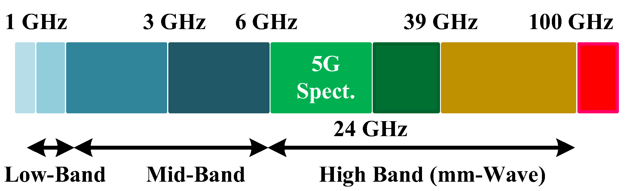
Nowadays, the frequency band of fourth Generation wireless systems (4G) is almost saturated. As shown in
Figure 1, the fifth Generation of wireless systems (5G) offers a high data-rate communication, and the operating frequency has been extended to the mm-Wave band, due to its large bandwidth. Therefore, the design of mm-Wave integrated circuits has become popular in the last decade.
Phase-Locked Loops (PLL) and frequency multipliers are widely used for the generation of a high-frequency clock from a low-frequency clock, to ensure the synchronized operation of different blocks [
1]. Alternatively, in a Radio Frequency (RF) and mm-Wave transceiver [
2], PLL provides the local oscillator signals (LO) for the up- and down-conversion of the RF signals.
Figure 2 shows the well-known top block diagram of an analog PLL. As an essential building block of an analog PLL inside the transceiver architecture, a wide tuning range and low phase noise Voltage Controlled Oscillator (VCO), operating at a higher frequency, is highly demanded. The phase noise of the VCO results in leakage of power into adjacent channels, as well as interference, and also enhances the bit error rate in digital communication. On the other hand, a low phase noise design cannot satisfy the error vector magnitude (EVM). Therefore, a wide tuning range with low phase noise is a trending demand of such applications. Recently, to achieve a wide range and low phase noise at the same time, several techniques, such as capacitive and inductive tunings, have been reported. By using a combination of the switched capacitor bank for coarse tuning and the Metal Oxide Semiconductor (MOS) varactor for fine-tuning, a wide tuning range can be obtained [
3,
4]. However, in the mm-Wave frequency band, due to the capacitor and varactor, the quality factor of the Inductor and Capacitor (LC) tank decreases.
Another work [
5] employs the inductive tuning technique and uses switches at different locations in the secondary coil to increase the number of sub-bands and the resulting wide tuning range. A large number of switches on the coil path introduces more parasitic capacitance, and the parasitic capacitance of switches highly affects the overall performance.
The work proposed in [
6] utilizes a topology based on triple-coupled inductors, which are used to couple three pairs of varactors and compensates for the tuning nonlinearities of the LC tank, while achieving a tuning range of 15.8%, with the center frequency of 20.85 GHz. Simulation and measurement results show the phase noise performance has not been improved sufficiently. In contrast, the design of a wide-range and low phase noise VCO would be difficult, considering the trade-offs between the tuning range, phase noise and power consumption. On the other hand, the design process at higher frequencies becomes more complicated when the layout parasitic effects come into play.
In this brief, a wide tuning range and low phase noise VCO is proposed. Since in a CMOS VCO the phase noise is limited by the oscillation amplitude and device noise, the transconductance linearization technique is employed to provide sufficient signal swing and low device noise. Coarse and middle switched capacitor arrays are provided to cover the whole frequency range, of 14 GHz to 18 GHz, while the varactor offers continuous fine-tuning. The switch sizes inside the switch capacitor array are optimized to lower the introduced flicker and channel noise, while keeping the frequency range wide. A new layout technique is employed to shrink the VCO output routing and resistance, which prevents the reduction of the quality factor of the Inductor and Capacitor (LC) tank.
The rest of this paper is organized as follows:
Section 2 describes VCO implementation, with the transconductance linearization technique and capacitive tuning method. Post-layout simulation results are presented in
Section 3. The conclusion of the paper is summarized in
Section 4.
2. VCO Implementation with Linearized Transconductance and Capacitive Tuning
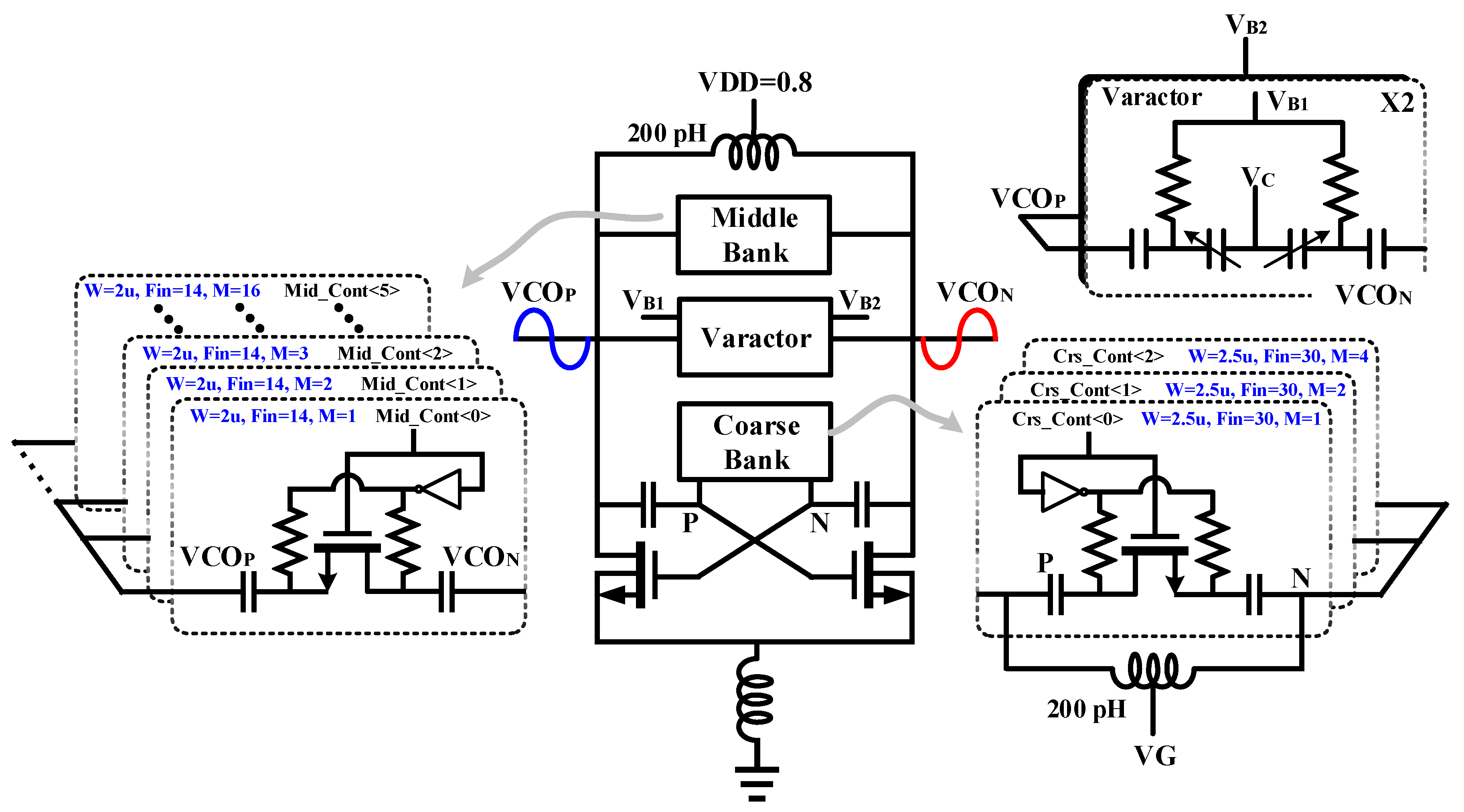
Figure 3 indicates the schematic of the proposed VCO with the linearized transconductance technique. The oscillation condition of an LC-based VCO can be represented as (1):
where
and
are the transconductance of the active part and equivalent resistance of the passive part, respectively.
In an LC-VCO, considering the noise produced by the parasitic resistance and cross-coupled pair as presented in [
7], the output noise can be driven as in Equation (2):
where
and
are Boltamann’s constant, temperature, parasitic resistance, and multiple noise factor of the cross-coupled pair, respectively. Therefore, the ratio of the output noise and signal power is equal to (3):
As can be easily observed, increasing the oscillation amplitude improves the phase noise performance of the VCO effectively. For a given current, the class-C VCO provides high oscillation amplitude characteristics. In the proposed architecture, the maximum achievable oscillation amplitude, through the famous saturation condition
, can be obtained, wherein
, and
are the Drain, Gate and threshold voltages, respectively. When the Drain voltage is minimum, the Gate voltage is maximum, and A represents the voltage gain from Gate to Drain of the feedback path, Equations (4) and (5) can be realized.
As can be seen, if the gate of the cross-coupled pair is biased at lower voltages, the proposed architecture provides a larger oscillation amplitude. According to Equation (5), if the gate of the cross-coupled pair is directly connected to the LC tank, to keep the transistors out of the triode region, the oscillation amplitude should be small. In this case, the amplitude is not allowed to be more than V
th/2. As shown in
Figure 4, the DC isolation of the Gate and Drain through the coupling capacitance lets the Gate be biased lower than the Drain, thereby reducing the nonlinearity of the active part. Besides, this provides a high efficiency of DC current conversion into class-C current waveforms, and minimizes the generation of effective noise. The
drops with increasing oscillation amplitude, and cross-coupled pairs become nonlinear when entering the deep triode region. The
determines the active part noise power at the zero-crossing point, where the sensitivity of the phase noise is high [
8]. Therefore, the proposed technique shrinks the operation of the LC-VCO in the triode region by extending the saturation region.
In contrast, the transconductance linearization approach optimizes the design by eliminating the deep triode region, introducing larger amplitude, lowering noise generation, and improving the quality factor of the tank compared to conventional LC-VCOs.
The sizes of the cross-coupled pairs are chosen to be large enough to provide almost ideal switch characteristics. Since the topology provides high swing, the VDD is 0.8 V, and considering the tank load, its safe operation, which avoids Gate-breakdown inside the frequency tuning range, is guaranteed.
The trade-off between the quality factor of the switched capacitor bank and VCO’s tuning range is an unavoidable issue in wide tuning range VCOs. The MOS switches introduce on-resistance in the signal path, which lowers the quality factor of the tank. To lower the on-resistance of the switch, a MOS transistor with a large size is required, considering the reduction of phase noise. The large sized MOS transistor introduces parasitic capacitance, and limits the tuning range of the VCO. Hence, for a wide tuning range, small size transistors are preferred.
As shown in
Figure 5, the switched capacitor quality factor (
), when the switch is on, is proportional to Equation (6):
where the value of
can be calculated through Equation (7).
where
and
are the mobility of the carrier, oxide capacitance, width, length, and the threshold voltage of the NMOS switch, respectively.
Also, in the off state, the equivalent capacitance
is equal to Equation (7):
Therefore, the switch size and the value of should be chosen carefully to minimize the on-resistance of the switch, while keeping the frequency range wide. Since the frequency steps and the fixed unit capacitor of the coarse stage are large, the switch sizes in this stage are selected to be large enough to minimize the on-resistance. Besides, the switch sizes for the middle capacitor array are optimized through noise analysis, to make their noise contribution less than 2%.
As shown in
Figure 3, the discrete frequency tuning of the VCO is realized by using 3-bits coarse and 6-bits middle tunings. The varactor offers a continuous frequency tuning range of 160 MHz/V at the center frequency of 16 GHz. Higher VCO gain (KVCO) needs a larger fixed capacitor inside the varactor, and introduces large AM (Amplitude modulation) to FM (Frequency modulation) noise. Therefore, the size of the capacitance of the varactor, or the value of KVCO, can be relaxed, while this capacitance can be compensated by increasing the size of the switches in both coarse and middle tuning stages. The middle capacitor bank and varactor are located at the Drain since the variation of the capacitance is less than that of the Gate. Two resistors inside the switched capacitor are provided to isolate the AC of the VCO nodes. To lower the thermal noise of the resistor inside the switched capacitor, its size is optimized to make the noise contribution less than 1%.
The tail inductor resonates with the parasitic capacitance of the tail node (2w0), and prevents the loading of the tank when one of the cross-coupled transistors enters the triode region, thereby improving phase noise. This method also enhances the linearity of the cross-couple transistors and lowers the current harmonics.
Figure 6 shows the schematic and simulated environment of the designed inductive buffer. In a transceiver, the buffer isolates the VCO from the other signal path of the transceiver. At both inputs of the buffer, AC coupling capacitors are provided to block the DC components of the AC waveform, so that the buffer remains correctly biased through the provided resistors R1 and R2. The switched capacitor adjusts the output swing of the buffer, with consideration of the carrier frequency and Process, Voltage, and Temperature (PVT) variations.
As shown in
Figure 7a, the VCO routing introduces parasitic inductance and resistance, which lower the quality factor of the tank. In order to shrink the output routing, the input transistors of the VCO buffer are located as close as possible to the VCO output’s routing, as seen in
Figure 7b. Thus, utilizing this technique keeps VCO output routings short, and enhances the phase noise performance of the VCO by around 1 dBc/Hz at 1 MHz offset frequency. To suppress the parasitic resistance and inductance, the routing of VCO outputs is stacked through the wide metal 7 and 8. Via and wide metal lines tie the parasitic inductance in parallel. Therefore, the introduced parasitic inductance can be lowered effectively, and the VCO offers linear VCO frequency steps. The simplified pattern of the layout is shown in
Figure 7c.
3. Experimental Result
Figure 8 shows the top layout of the proposed VCO. It consists of VCO core, tail inductor, VCO buffer and test buffer, and occupies a layout area of 0.14 mm
2. The circuit is implemented in a 40-nm CMOS process. The VCO core consumes 24 mW from the power supply of 0.8 V, while inductive buffers consume 21 mW from the power supply of 1.1 V. The VCO operation is verified through the Electro-Magnetic (EM) based post-layout simulation. The proposed VCO satisfies the frequency range of 13 GHz to 19 GHz in all corner cases and temperatures, while the target frequency range is from 14 GHz to 18 GHz. The additional 2 GHz frequency range is considered for variation of the capacitors inside the switch capacitor bank during the fabrication process. The tuning range of the VCO can be calculated through Equation (8):
Therefore, the proposed VCO offers the tuning range of 37.5%.
Figure 9 demonstrates the linearity and discrete tuning of the coarse and middle switched capacitor banks of the proposed VCO. In this simulation, the binary controlling bits of the coarse bank are changed from 001 to 100 (1 to 4 decimal), while the 6 bits of the middle capacitor array are adjusted from all “0” to all “1”, within each code of the coarse bank. The maximum frequency resolution of the middle capacitor bank at 18 GHz is 100 MHz, while with a decreasing frequency this frequency step decreases. To avoid any blind zones inside the frequency range, there are overlapped frequencies between the coarse and middle tunings. The weights of the capacitors inside the middle stage are 1, 2, 3, 4, 8 and 16. One redundant bit with the weight of 3 is considered to avoid any blind zones inside the middle-frequency range.
Figure 10 indicates the continuous tuning of the VCO through controlling the voltage of VC. As the simulation results show, the VCO gain is 120 MHz/V, 180 MHz/V and 300 MHz/V, at 14 GHz, 16 GHz and 18 GHz, respectively.
Figure 11 shows the phase noise performance of the linear transconductance VCO at 14 GHz and 18 GHz carrier frequencies. The post-layout simulation results of phase noise at 14 GHz are −87.2 dBc/Hz, −113 dBc/Hz and −134 dBc/Hz at 10 kHz, 1 MHz and 10 MHz offset frequencies, respectively. The VCO offers phase noise performance of −87.4 dBc/Hz, −110 dBc/Hz and −130 dBc/Hz for 10 kHz, 1 MHz and 10 MHz offset frequencies at 18 GHz carrier frequency.
Figure 12 shows the transient simulation result and output swing of the VCO with output buffers at 14 GHz and 18 GHz, respectively. In this simulation, the load condition for the test buffer is the coupling capacitance and a 50-ohm load, and the VCO buffer is simulated considering the input load of the divider.
Table 1 summarizes the performance of the proposed VCO in different corners and temperatures. The results show that the variation of the phase noise in all corner conditions is less than 3 dBc/Hz, at the start and end of the frequency.
Table 2 features the proposed VCO as well as the recent works. It should be noted that the comparison with the fabricated works is not fair. However, the phase noise is calculated in the presence of the Low Dropout regulator (LDO) noise, considering the loading effect of the coupling capacitance, 50-ohm load, and the input load of the divider inside the PLL. Further, the frequency range of the VCO is optimized using the EM-based post-layout simulation results. Therefore, the provided simulation environment provides a fairer evaluation compared to the practical conditions.
To evaluate the performance of the VCO, the Figure of Merit (FoM
T) is presented in Equation (9).
where the
,
are the phase noise, center frequency, offset frequency from the carrier frequency, frequency tuning range and power consumption, respectively. The proposed VCO indicates superior performance to those of previous works for wide range applications.


