Article

New Insight on Terahertz Rectification in a Metal–Oxide–Semiconductor Field-Effect Transistor Structure

Department of Information Engineering, Electronics and Telecommunications, Sapienza University of Rome, 00184 Rome, Italy
Electronics 2020, 9(7), 1089; https://doi.org/10.3390/electronics9071089
Submission received: 27 May 2020 / Revised: 28 June 2020 / Accepted: 30 June 2020 / Published: 3 July 2020
(This article belongs to the Section Microelectronics)

Abstract

:
The use of a metal–oxide–semiconductor field-effect transistor (MOS-FET) permits the rectification of electromagnetic radiation by employing integrated circuit technology. However, obtaining a high-efficiency rectification device requires the assessment of a physical model capable of providing a qualitative and quantitative explanation of the processes involved. For a long time, high-frequency detection based on MOS technology was explained using plasma wave detection theory. In this paper, we review the rectification mechanism in light of high-frequency numerical simulations, showing features never examined until now. The results achieved substantially change our understanding of terahertz (THz) rectification in semiconductors, and can be interpreted by the model based on the self-mixing process in the device substrate, providing a new and essential tool for designing this type of detector.

1. Introduction

The terahertz (THz) radiation spectrum covers the gap between microwaves and infrared regions. Since THz radiation is non-ionizing and the associated power is low, it is considered medically safe. Furthermore, the THz wavelength is able to deeply scan under the surface of materials under investigation. The resulting combination of safety and penetration can be a winning quality in different applications, such as medical imaging, security/surveillance imaging, and spectroscopic applications. The detection of high-frequency electromagnetic radiation, in particular THz, using integrated commercial electronics represents a challenge that is pushing great experimental and theoretical activities, with the goal of achieving high-resolution images, high sensitivity, and low cost. Recently, there has been a strong effort to achieve THz sensors using standard complementary metal–oxide–semiconductor (CMOS) technology, taking advantage of robust and reproducible devices at low cost. Recent reviews help to highlight the exceptionally rapid progress of THz science and technology [1,2,3,4,5,6,7].
In particular, combining all these characteristics could allow the realization of detector arrays up to whole panel scale, achieving a wide area detection approach. In this scenario, a reliable model of the structure taking into account the rectification process is necessary for proper support of detector design.
To date, the universally recognized model for THz detection by use of a metal–oxide–semiconductor field-effect transistor (MOS-FET) is the one by Dyakonov and Shur [8], often referred to as the plasma wave model. The model, initially derived for two-dimensional (2D) electron gas, has also been extensively used and widely developed by many authors for the MOS-FET structure [9,10].
According to this model, when the radio frequency (RF) radiation impinging on the antenna produces a voltage drop between the gate and source electrodes of the MOS-FET, waves of carriers are generated in the 2D electron gas in the inversion layer of the transistor. The nonlinearities present in the semiconductor equations give rise to DC photovoltage. Recently, a new approach was developed, referred to as a self-mixing model in the substrate, showing how the presence of an RF electric field in a depletion region of a semiconductor can also produce DC photovoltage. This result was first achieved in studying a double barrier structure [11], then was extended to the single barrier present in a unidimensional MOS structure in the depletion condition [12].
In this paper, we use two-dimensional numerical simulation by technology computer-aided design (TCAD) software to study the rectification process inside the structure. This approach allows us to highlight features never examined until now, shedding new light on the mechanisms of rectification.

2. Analytical Interpretation and Numerical Simulator

In order to give a detailed description of the harmonic generation in the semiconductor based on the hydrodynamic equations, we can refer to a recent paper [13]. Here we prefer an intuitive approach, by describing an analytical solution that contains the first-order approach of the harmonic balance method. This description may help readers to better understand the simulation process.
It is demonstrated that the self-mixing effect and the rectification due to nonlinearity of equations are mainly related to the majority carriers. Assuming a p type substrate, we know that the hole continuity equation contains a nonlinearity, in particular in the first right-side term:
d p d t = p v p x + D p 2 p x 2
where p and vp are the total hole density and velocity, respectively, and Dp is the hole diffusion coefficient. In principle, the Euler equation also contains one nonlinear term; nevertheless, it can be neglected, particularly within the depletion region of a semiconductor [11]. If a sinusoidal voltage is applied to the gate,   V G ( t ) = V ^ G e j ϖ t , with V ^ G representing amplitude and ϖ the angular frequency of the signal, the quantities involved in the semiconductor generate sinusoidal variations, which are added to the equilibrium values. In the small signal approximation, Equation (1) becomes
j ϖ p ^ = [ v ^ p p 0 x + p ^ v p 0 x + v p 0 p ^ x ] + D p 2 p ^ x 2
where the nonlinear term of Equation (1) gives rise to three terms, once the physical quantities are approximated to the first-order variations, assuming a small signal. In this elaboration, following [13], the amplitude of velocity variations, v ^ p , is assumed to be spatially constant in the depletion region. Once the first-order solution of hole variations is obtained from Equation (2), the expression can be substituted into the nonlinear term in Equation (1). The time average of the carrier fluxes give rise to a DC self-mixing term J D C p = q p v p , i.e., a non-homogeneous term which must be added to the DC current balance equations, as given by
J D C p + q p v p q D p X d p d x = 0
In principle, the nonlinear term in Equation (1) also gives rise to a second-order non-homogeneous term; further interactions may also give rise to higher-order terms.
Equations (1)–(3) must be solved in the spatially distributed structure under study. TCAD solves this problem using finite differences approximation of the equation in 2D and 3D structure, also giving the higher-order harmonic generation, either inside the structure or as currents and voltages at the electrodes. The TCAD Sentaurus Device [14] in particular performs simulations using the hydrodynamic equations, based on the work of Stratton [15] and Bløtekjær [16], adopting a simplified approach of six partial differential equations (PDEs) [17].
From TCAD, we use in particular harmonic balance analysis, which takes into account the nonlinearities present in the semiconductor equations, and furnishes the distributions of all semiconductor quantities inside the structure at different harmonics. The zero-frequency term of the harmonic balance, so-called C0, furnishes the variations produced in the steady state condition by the self-mixing effect.
The TCAD simulator has been widely used in attempts to evaluate the MOS-FET rectification process, with different approaches. In Reference [18], the characterization was conducted in transient time by an examination of the drain voltage, extracting DC and harmonics by Fourier transform. In References [19,20] the quasi-plasma 2D capability of TCAD Sentaurus was used, with the specific intention to limit the interaction occurring between the carriers and the RF field to the channel zone. In Reference [21], the bell shape response of the voltage at the drain versus the gate bias voltage was extracted from two-dimensional simulations. In this work, unlike previous attempts, we used the analysis of harmonic balance as the main tool.
Using TCAD, we show that rectification photovoltage arises mainly in the depleted region under the gate oxide, thus confirming the one-dimensional model prediction. In addition, the two-dimensional nature of the TCAD analysis permits us to evaluate how the charge displacement generated by the self-mixing effect, dielectrically coupling toward the doped regions under the contacts, can be held as the origin of the transient currents detected in several measurements performed on MOS-FET at THz frequencies.

3. Simulation of THz Rectification in MOS-FET Structure

For the simulations, we adopted the structure of a MOS transistor with a 130 nm n-channel, derived from the one offered in the TCAD manual [14]. The source and drain diffusions have a phosphorus doping concentration of 1020 cm–3, with a lightly doped diffusion (LDD) implantation of 1018 cm–3. The polysilicon gate is assumed to be doped with phosphorus at 1020 cm–3. Figure 1 describes the device structure used in the simulations, indicates the dimensions of the channel, and the reference axes.
We assumed a substrate boron doping concentration of 5 × 1018 cm–3 in order to ensure a dielectric relaxation frequency higher than 1 THz and concentrate the RF electric field in the depleted region just below the gate. The transistor dimensions are much smaller than the RF wavelength (at 1 THz, = 300 m), so the fringes of the electric field almost completely wrap the semiconductor structure. In particular, the RF electric field homogeneously crosses the depleted region under the gate, and thus interacts there with carriers.
We considered a short-circuit to ground the source and connected the drain to a 1 MΩ resistance toward the ground in order to reproduce the configuration usually adopted in the measurements reported in the literature.

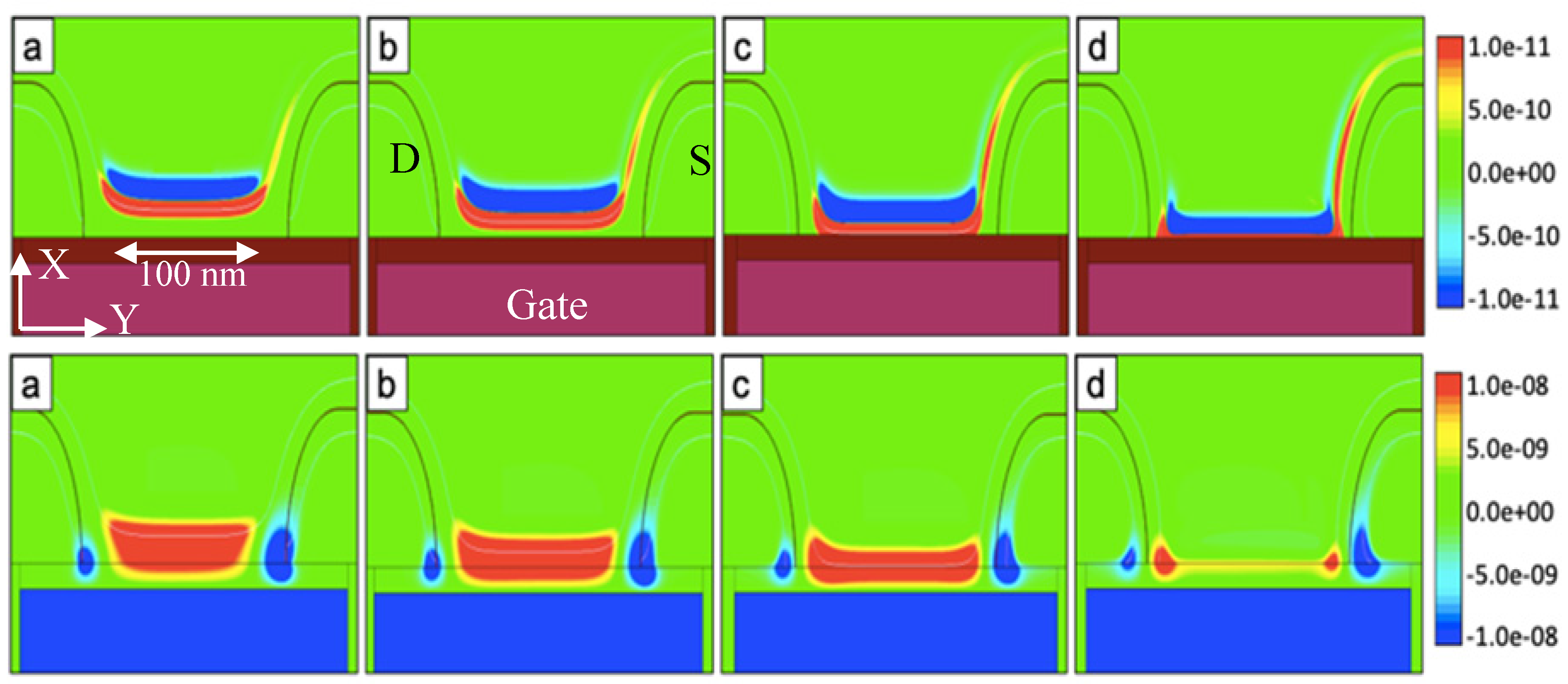
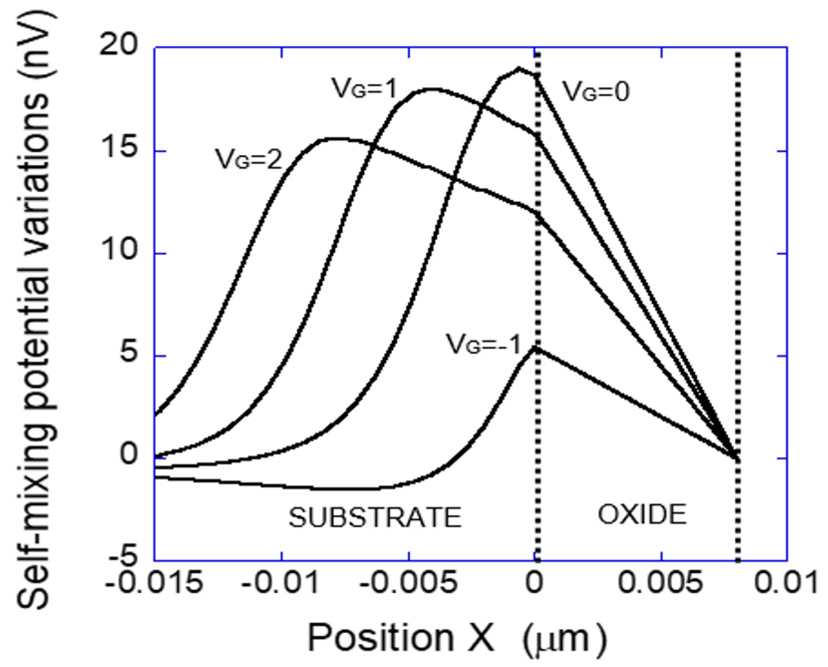
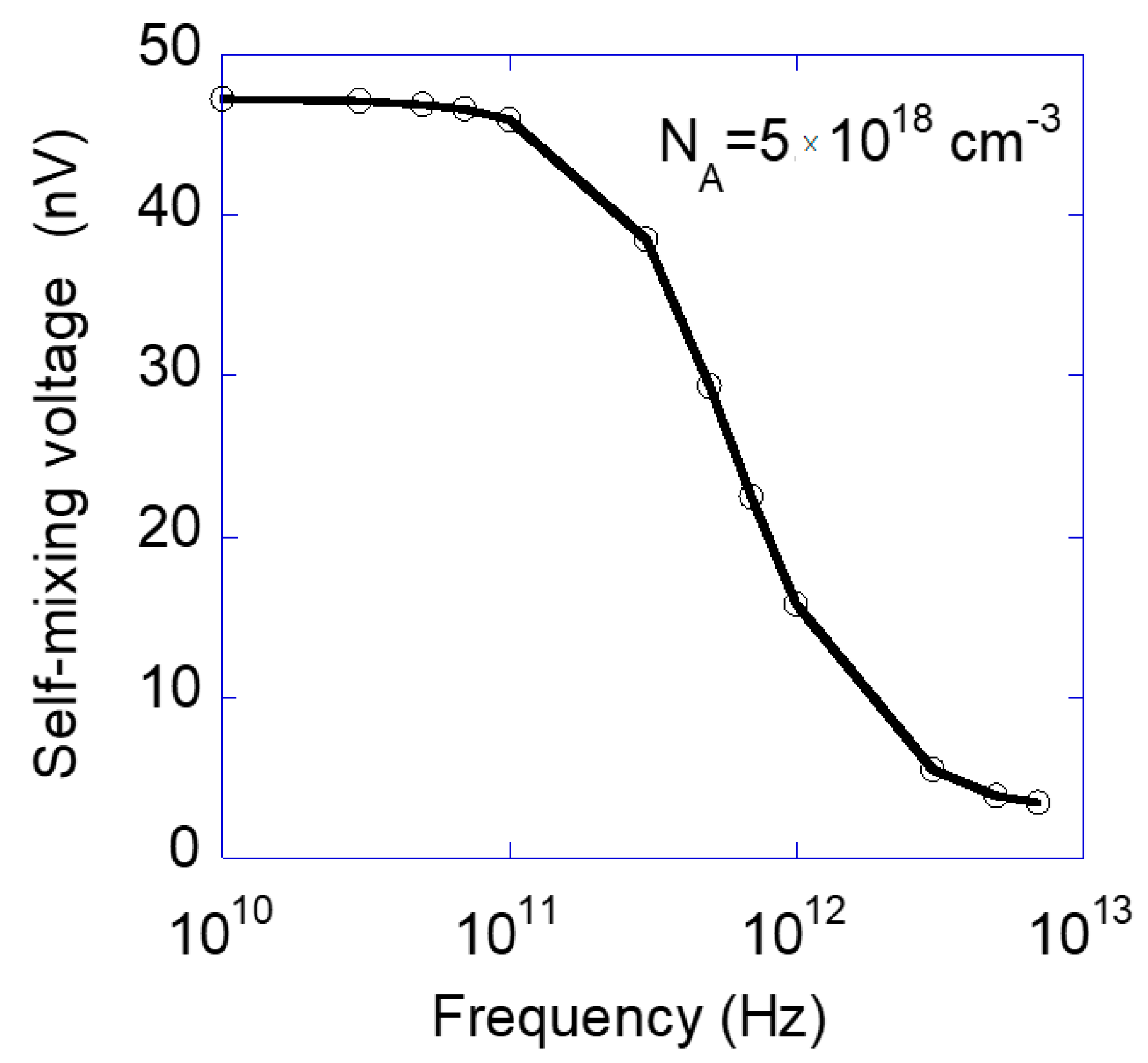
3.1. Self-Mixing Effects Iside the Silicon Structure

Among the semiconductor variables, we searched DC changes in particular, with respect to the steady state conditions, under the application of RF sinusoidal voltage at the gate. These variations represent the result of the nonlinear interaction of the electric field, with the carrier and the self-mixing. In the TCAD program, they are referred to as C0 solutions of the harmonic balance analysis.
Figure 2 shows an initial set of variations induced by the self-mixing in different bias conditions; the steady state value was subtracted. All variations are in DC conditions.
In all panels, the drain is on the left side and the source on the right side, as indicated in panel b. Panel a reports the directions of the reference axes and indicates the dimension of channel length. The thin white lines indicate the nominal position of the depletion edge.
The top row of Figure 2 reports the simulation results of the variation of DC hole density due to the application of 1 mV amplitude voltage at a frequency of 1 THz, with a bias voltage at the gate as follows: (a) VG = 2 V, (b) VG = 1 V, (c) VG = 0 V, and (d) VG = −1 V. We note that with the chosen doping, the structure has a flat band voltage of −0.09 V.
We can observe the presence of a dipole of charge, with an increase of hole density, namely the h+ area, located beside the gate. In the color scale, red indicates positive variations. This charge is coupled a short distance from a region of decreased hole density, namely the h− area, indicated by blue.
The formation of a charge dipole in the substrate, within the depletion layer, is predicted by the one-dimensional self-mixing model in the substrate [13], due to a net flux of holes and majority carriers pushed from the body of the semiconductor toward the depleted region by the nonlinear interaction of carriers with the RF.
We can see how the width of the depletion region is reduced with the decrease in gate voltage, and at the same time the dipole flattens out against the oxide surface. This last aspect follows the predictions of the one-dimensional self-mixing model, which limits the rectification effect to the depleted layer, which is a progressively smaller region when VG is reduced closer to the oxide.
The bottom row of Figure 2 shows the corresponding variation of DC potential, while Figure 3 reports the Y cut of these distributions along a vertical line from the gate toward the body at the center of the structure for the four gate voltage values. Again, as expected from the analytical model [13], both the maximum variation of DC potential and its value at the interface with the oxide increase with the decreasing size of the depletion region, as explained by the intensification of the RF electric field. In particular, this is evident in observing the sequence represented by cases a, b, and c. In the accumulation condition, case d, a relevant increase of negative potential is observed in the semiconductor body, but we notice that in this condition the model [13] is no longer valid.
The charge displaced in the depletion region by the self-mixing effect is electrostatically coupled in part with the charge accumulated at the gate, through the oxide barrier, and in part at the source and drain diffusions, through the junction barriers. Only part of the dipole charge is coupled with charges accumulated in the substrate.
Figure 4 shows an X cut of the distributions of potential obtained with the four values of gate voltages. The cut is at x = 0, beside the silicon–oxide interface. Dotted lines represent the nominal position of the edges of the lightly doped diffusion implantations, which limit the channel at length Lch = 100 nm.
We notice that the variation of potential occurring within the channel is very limited; accordingly, the potential at the drain is extremely limited. Much larger potential accumulates toward the surface of the silicon from the substrate.
Some of the particulars of these curves can be explained surprisingly well by the model of self-mixing in the substrate [13]. For example, there are strong dipolar variations of the potential next to the junctions of drains and sources. Since the RF electric field crosses these regions, the feature can thus be interpreted as photovoltage generated by the self-mixing effect occurring in the depleted regions of the contact regions at the edges of the channel holes from the substrate, and electrons from the doped zones are pushed toward the center of each junction, creating two local dipoles.
Positive peaks due to holes are present mainly in the accumulation condition, VG = −1, i.e., when holes are present at the interface; the peaks disappear when the generation of photovoltage is moved toward the substrate by depletion of the surface. Moreover, the source barrier is crossed by a stronger field since that contact is grounded; therefore, the photovoltage, due to electrons, is larger at that side.
On the contrary, there is almost no evidence of potential growth along the silicon–oxide surface, i.e., along the MOS-FET channel, as predicted by the Dyakonov and Shur model [8].

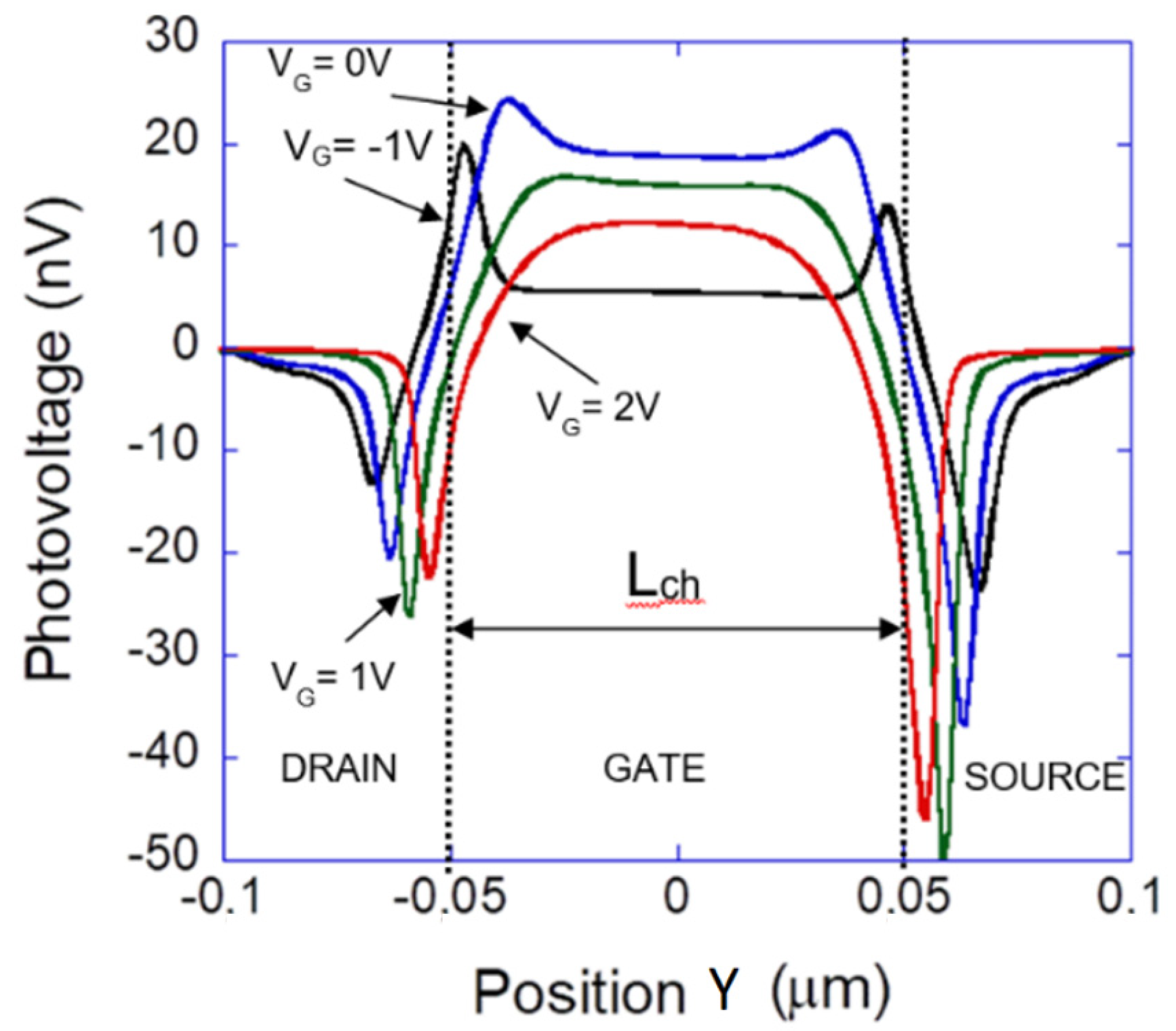
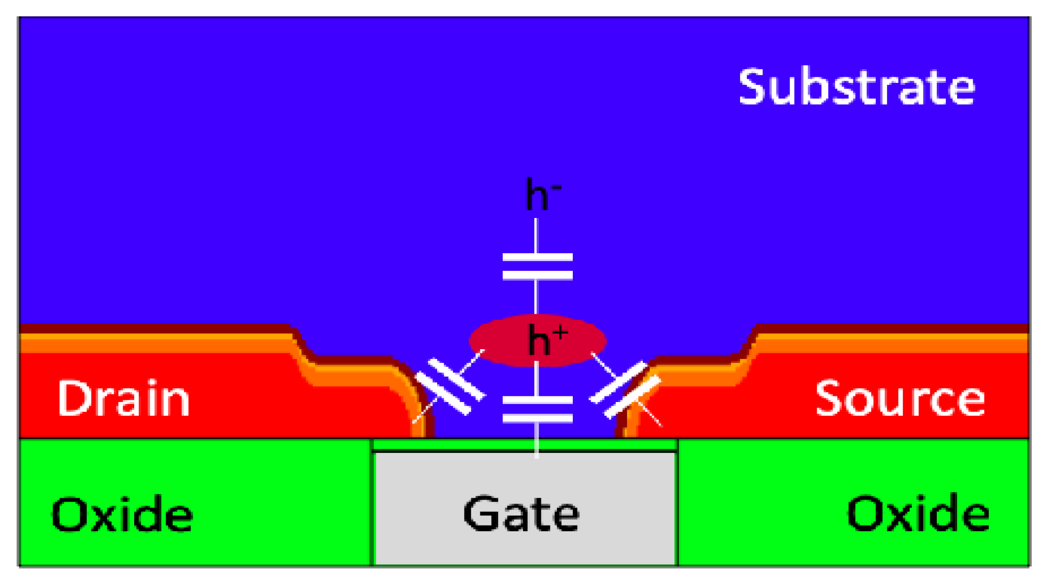
3.2. Rectification Effects at the Contacts

We have shown that the greatest contribution to the generation of photovoltage under THz radiation is in the substrate of the MOS-FET structure, within the depletion region, due to the accumulation of holes by the self-mixing effect under RF penetration.
In the case of a MOS-FET, we must consider that the accumulated charge faces a two-dimensional structure; thus, h+ charges are electrostatically coupled, in part with charge accumulated at the gate through the oxide barrier, in part at the source and drain diffusions through the junction barriers. Only part of the charge of the dipole is finally mirrored by accumulated charges in the substrate, in zone h−. The coupling effects are schematically described in Figure 5, indicated as parasitic capacitance.
It is extremely important to verify the effect at the contacts and determine the relationship between the variation induced inside the structure and the external measurable quantities. In this regard, harmonic balance analysis has some limitations, since it represents an equilibrium state; thus, the barriers to the contacts and the oxide toward the gate do not allow the photocurrent to flow externally. Simulations thus seem to be unable to reproduce the measurements reported in the literature, which indeed are always performed in transient conditions, under chopped radiation and using the lock-in technique.
In order to overcome this limitation, we chose to observe the second harmonic external voltage, considering it a good approximation of the photovoltage measured in transient conditions. The two photovoltages indeed originate from the same nonlinear term in Equation (1), which gives rise to two terms with the same spatial distribution, at second harmonic and DC (zero order). Then, the two terms are entered in the respective current equations. Naturally, the boundary conditions are different, since capacitance does not block the passage of current at twice the fundamental frequency, while at DC it allows the current to flow only during charging of the parasitic capacitance of the measurement setup. This consideration suggests that the second harmonic can be considered as an evaluation of the behavior of the DC term during transient measurements, when the parasitic capacitance gets charged.
In particular, Figure 6 reports all currents at the electrodes obtained from the second harmonic as an effective estimation of the detection sensitivity. It appears evident that the current at the gate (IG) is much larger than the current measured either at the source (IS) or body (IB) (black lines), which are in short circuit condition, than at the drain (ID, red line) loaded with 1 M resistance. We notice that the voltage detected by measurements, in particular by the lock-in amplifier, is the effect of the charging of the external circuit, including cable and amplifier parasitic capacitance, by these self-mixing photocurrents.
The maximum value of the detectable voltage can only be reached if the parasitic capacity of the acquisition system is zero; in this case, it would be equal to the DC voltage across the oxide capacitance. The flatness of the potential at the interface permits an approximation to a plane capacitor of the coupling between the dipole and the gate electrode, and thus assumes the voltage across the oxide as the value of potential at x = 0, y = 0. We cannot use a similar approach to evaluate the voltage at the drain, since the coupling between the dipole and the doped drain region is obtained by a two-dimensional distribution of charge, which cannot be evaluated in any heuristic way. The author thus chose to evaluate it as the value of potential at the drain at the second harmonic. Also, in this case, the parasitic capacitance is assumed to be zero.
Figure 7 reports an evaluation of the responsivity obtained by calculating the two potentials. To this aim, the author followed the procedure in [22], given the value of the real part of the AC conductance at the gate GD = 2 × 10⁻⁶ Ω−1 obtained from TCAD simulations, and the applied value of 1 mV RF voltage. It can be observed that both curves present bell-shaped dependence versus the applied gate voltage, which is characteristic of MOS-FET detection. Both the bell-shaped curves and the absolute values are coherent with several measurements reported in the literature, all with detection at the drain (e.g., [9,22,23,24]). The author notes that even if the measurements at the drain are almost exclusively present in the literature, the reported results indicate that detection at the gate is dramatically more effective, thus offering a strong possibility of development of the technique.
Finally, Figure 8 reports the simulation of the frequency behavior of the self-mixing potential at the interface between silicon and oxide (x = 0). The detection voltage presents a cutoff frequency of around 200 GHz. This result is strictly dependent on the substrate doping, and is coherent with results shown in [13] on elementary MOS capacitance.

4. Conclusions

This paper presents numerical TCAD simulations of the nonlinear interaction of an electromagnetic field at 1 THz in the MOS-FET structure. The use of two-dimensional simulations offers pictorial images of the RF interaction with the semiconductor, which should overcome years of heuristic assumptions. This ensured a rigorous physical approach, guaranteed by a robust simulation environment, independent from analytical approximations. The paper shows that rectification occurs mainly within the depletion layer under the gate, producing a change of the DC charge distribution and a coupling of this charge toward the electrodes of gate, source, drain, and body, showing features never examined until now. The coupling through the gate turned out to be the most effective by far. Moreover, understanding that the output signal is due to the internal photocurrent gives a completely different approach to the design; in particular, the area of the device does not limit the charge transit time and thus it can be increased in order to make the charging of the parasitic capacitance of the sensing amplifier more effective. The results put under discussion the well-known plasma-wave model, while confirming the prediction of the self-mixing model, thus substantially improving our understanding of the THz rectification process.

Funding

This research was funded by Italian PNRM E.F. 2018 n a2017.153M, Contract n. 2013a, 20.12.2018.

Acknowledgments

The author acknowledges the support of Ing. Paola Piedimonte in performing the TCAD simulations.

Conflicts of Interest

The author declares no conflict of interest.

References

  1. Guerboukha, H.; Nallappan, K.; Skorobogatiy, M. Toward real-time terahertz imaging. Adv. Opt. Photon. 2018, 10, 843–938. [Google Scholar] [CrossRef]
  2. Islam, M.S.; Cordeiro, C.M.; Franco, M.A.; Sultana, J.; Cruz, A.L.; Abbott, D. Terahertz optical fibers. Opt. Express 2019, 28, 16089–16117. [Google Scholar] [CrossRef] [PubMed]
  3. Zaytsev, K.I.; Dolganova, I.N.; Chernomyrdin, N.V.; Katyba, G.M.; Gavdush, A.A.; Cherkasova, O.P.; Komandin, G.; Shchedrina, M.A.; Khodan, A.N.; Ponomarev, D.S.; et al. The progress and perspectives of terahertz technology for diagnosis of neoplasms: A review. J. Opt. 2019, 22, 013001. [Google Scholar] [CrossRef]
  4. Smolyanskaya, O.; Chernomyrdin, N.; Konovko, A.; Zaytsev, K.I.; Ozheredov, I.; Cherkasova, O.P.; Nazarov, M.M.; Guillet, J.-P.; Kozlov, S.; Kistenev, Y.V.; et al. Terahertz biophotonics as a tool for studies of dielectric and spectral properties of biological tissues and liquids. Prog. Quantum Electron. 2018, 62, 1–77. [Google Scholar] [CrossRef]
  5. Yachmenev, A.E.; Lavrukhin, D.V.; Glinskiy, I.A.; Zenchenko, N.V.; Goncharov, Y.G.; Spektor, I.E.; Khabibullin, R.A.; Otsuji, T.; Ponomarev, D.S. Metallic and dielectric metasurfaces in photoconductive terahertz devices: A review. Opt. Eng. 2019, 59, 061608. [Google Scholar] [CrossRef]
  6. Yachmenev, A.E.; Pushkarev, S.S.; Reznik, R.R.; Khabibullin, R.A.; Ponomarev, D.S. Arsenides-and related III-V materials-based multilayered structures for terahertz applications: Various designs and growth technology. Prog. Cryst. Growth Charact. Mater. 2020, 66, 100485. [Google Scholar] [CrossRef]
  7. Lepeshov, S.; Gorodetsky, A.; Krasnok, A.; Rafailov, E.U.; Belov, P. Enhancement of terahertz photoconductive antenna operation by optical nanoantennas. Laser Photon. Rev. 2016, 11, 1600199. [Google Scholar] [CrossRef] [Green Version]
  8. Dyakonov, M.; Shur, M. Detection, mixing, and frequency multiplication of terahertz radiation by two-dimensional electronic fluid. IEEE Trans. Electron Devices 1996, 43, 380–387. [Google Scholar] [CrossRef]
  9. Al Hadi, R.; Sherry, H.; Grzyb, J.; Baktash, N.; Zhao, Y.; Öjefors, E.; Pfeiffer, U. A broadband 0.6 to 1 THz CMOS imaging detector with an integrated lens. In Proceedings of the IEEE MTT-S International Microwave Symposium, Baltimore, MD, USA, 5–10 June 2011. [Google Scholar]
  10. Lisauskas, A.; Pfeiffer, U.; Ojefors, E.; Bolívar, P.H.; Glaab, D.; Roskos, H.G. Rational design of high-responsivity detectors of terahertz radiation based on distributed self-mixing in silicon field-effect transistors. J. Appl. Phys. 2009, 105, 114511. [Google Scholar] [CrossRef]
  11. Palma, F.; Rao, R. A model of high-frequency self-mixing in double-barrier rectifier. J. Infrared Millimeter Terahertz Waves 2018, 39, 422–438. [Google Scholar] [CrossRef] [Green Version]
  12. Palma, F.; Rao, R. Terahertz detection in MOS-FET: A new model by the self-mixing. In Proceedings of the 43rd International Conference on Infrared, Millimeter, and Terahertz Waves (IRMMW-THz), Nagoya, Japan, 9–14 September 2018; pp. 1–3. [Google Scholar]
  13. Palma, F. Self-mixing model of terahertz rectification in a metal oxide semiconductor capacitance. Electronics 2020, 9, 479. [Google Scholar] [CrossRef] [Green Version]
  14. Synopsys Inc. Sentaurus Device, User Manual, Version Y-2006; Synopsys Inc.: Mountain View, CA, USA, 2006. [Google Scholar]
  15. Stratton, R. Diffusion of hot and cold electrons in semiconductor barriers. Phys. Rev. 1962, 126, 2002–2014. [Google Scholar] [CrossRef]
  16. Blotekjaer, K. Transport equations for electrons in two-valley semiconductors. IEEE Trans. Electron Devices 1970, 17, 38–47. [Google Scholar] [CrossRef]
  17. Szeto, S.; Reif, R. A unified electrothermal hot-carrier transport model for silicon bipolar transistor simulations. Solid-State Electron. 1989, 32, 307–315. [Google Scholar] [CrossRef]
  18. Meng, Q.; Lin, Q.; Jing, W.; Han, F.; Zhao, M.; Jiang, Z. TCAD Simulation foe nonresonant terahertz detector based on double-channel GaN/AlGaN high-electron-mobility transistor. IEEE Trans. Electron. Devices 2018, 65, 4807–4813. [Google Scholar] [CrossRef]
  19. Hwang, H.C.; Park, K.; Park, W.; Kim, K.R. Design and characterization of plasmonic terahertz wave detectors based on silicon field-effect transistors. Jpn. J. Appl. Phys. 2012, 51, 06FE17. [Google Scholar] [CrossRef]
  20. Notario, J.A.D.; Meziani, Y.M.; Velázquez-Pérez, J.E. TCAD study of sub-THz photovoltaic response of strained-Si MODFET. J. Physics: Conf. Ser. 2015, 647, 012041. [Google Scholar] [CrossRef] [Green Version]
  21. Velazquez, J.E.; Fobelets, K.; Gaspari, V. Study of current fluctuations in deep-submicron Si/SiGe n-channel MOSFET: Impact of relevant technological parameters on the thermal noise performance. Semicond. Sci. Technol. 2004, 19, S191–S194. [Google Scholar] [CrossRef] [Green Version]
  22. Pfeiffer, U.R.; Ojefors, E. A 600-GHz CMOS focal-plane array for terahertz imaging applications. In Proceedings of the 34th European Solid-State Circuits Conference (ESSCIRC), Edinburgh, UK, 15–19 September 2008; pp. 110–113. [Google Scholar] [CrossRef]
  23. Tauk, R.; Teppe, F.; Boubanga, S.; Coquillat, D.; Knap, W.; Meziani, Y.M.; Maude, D.K. Plasma wave detection of terahertz radiation by silicon field effects transistors: Responsivity and noise equivalent power. Appl. Phys. Lett. 2006, 89, 253511. [Google Scholar] [CrossRef] [Green Version]
  24. Liu, Z.; Liu, L.; Zhang, Z.; Liu, J.; Wu, N. Terahertz detector for imaging in 180-nm standard CMOS process. Sci. China Inf. Sci. 2017, 60, 82401. [Google Scholar] [CrossRef]
Figure 1. The doping distribution in the device structure used in the simulations. The simulation program does not report the actual doping in the gate and in the oxide, treated as ideal.
Electronics 09 01089 g001
Figure 2. Top row: distribution of DC hole variations (scale bar: cm–3). The simulation program does not report hole variations in the gate and in the oxide both treated as ideal. Bottom row: potential distribution (scale bar: V) under 1 mV radio frequency (RF) gate voltage at 1 THz. Bias voltage at the gate: (a) VG = 2 V, (b) VG = 1 V, (c) VG = 0 V, (d) VG = −1 V.
Electronics 09 01089 g002
Figure 3. Distribution of DC potential generated by self-mixing in the substrate, shown along the Y cut at y = 0, under 1 mV RF gate voltage at 1 THz, at different gate voltages.
Electronics 09 01089 g003
Figure 4. Variation in DC of photovoltage along X cut, at x = 0 beside the silicon–oxide interface. Dotted lines represent the limits of the channel.
Electronics 09 01089 g004
Figure 5. Schematic of dielectric coupling of self-mixing dipole toward electrodes of the metal–oxide–semiconductor field-effect transistor (MOS-FET) device.
Electronics 09 01089 g005
Figure 6. Simulated second harmonic currents toward the four electrodes versus gate bias voltage at 1 THz.
Electronics 09 01089 g006
Figure 7. Responsivity calculated by the second harmonic voltage at drain (circles) and the DC voltage at the oxide interface (squares), plotted versus gate bias voltage.
Electronics 09 01089 g007
Figure 8. Frequency dependence of potential generated at silicon–oxide interface, y = 0, by self-mixing effect.
Electronics 09 01089 g008

