Article

A 4-mW Temperature-Stable 28 GHz LNA with Resistive Bias Circuit for 5G Applications

1
High-Frequency High-Voltage Device and Integrated Circuits R&D Center, Institute of Microelectronics, Chinese Academy of Sciences, Beijing 100029, China
2
School of Microelectronics, University of Chinese Academy of Sciences, Beijing 100029, China
*
Author to whom correspondence should be addressed.
Electronics 2020, 9(8), 1225; https://doi.org/10.3390/electronics9081225
Submission received: 3 July 2020 / Revised: 24 July 2020 / Accepted: 28 July 2020 / Published: 30 July 2020
(This article belongs to the Special Issue RF/Mm-Wave Circuits Design and Applications)

Abstract

:
This paper presents a low power two-stage single-end (SE) 28 GHz low-noise amplifier (LNA) in 90 nm silicon-on-insulator (SOI) CMOS technology for 5G applications. In this design, the influence of bias circuit is discussed. The 1200 Ω resistor which was adopted in bias circuit can feed DC voltage as well as keep whole circuit unconditionally stable. The gate bias points are set to 0.55 V to make the circuit low-power and temperature-stable. Measurement results illustrated that the LNA achieved a maximum small signal gain of 18.1 dB and an average 3.1 dB noise figure (NF) in operating frequency band. Measured S11 was below −10 dB between 25 GHz and 29 GHz and reverse isolation S12 was below −25 dB throughout the band. It consumed only 4 mW by proper selection of bias point with core area of 0.16 mm2 without pads. The fabricated LNA has demonstrated a gain variation of 3 dB and a NF variation of 1.9 dB from −40 °C to 125 °C with power variation of 0.8 mW. It suggests that the proposed SOI CMOS LNA can be a promising candidate for 5G applications.

1. Introduction

Recent years have witnessed the development of the fifth-generation wireless system (5G), which can provide higher data rate, lower delay and larger-scale equipment connection compared with 4G [1,2,3]. To achieve high data-rate and high resolution for numerous applications, such as augmented reality (AR), Internet of things (IOT), smart home, automatic driving, etc. [4], millimeter-band is introduced owing to its unique advantages. Results in our previous work [5] showed that the use of frequency band between 24 GHz and 29 GHz is prevalent. The band is considered as the most popular 5G band, and circuits working in this band are worthy of studying. In Figure 1, the diagram of 5G phased-array transceiver is present [6]. To realize the massive multiple-input multiple-output (MIMO) and phased array techniques, more than one transceiver (TRX) is integrated in the system [7]. Moreover, a temperature-stable TRX is always desirable for 5G applications. Under this circumstance, a compact LNA with small area and low power consumption while maintaining good performance even at different temperatures is necessarily required.
As a critical building block in the radio frequency front-end module, LNA is always expected to achieve certain gain without introducing much noise since it dominates the radio sensitivity [8]. Numerous researchers have studied LNA for 5G applications [6,9,10,11]. The III–V technologies like GaAs, InP, GaN, etc., were once the first choice due to their excellent-performance and high-efficiency [9], but the low integration level and high cost are insufferable. As a contrast, the burgeoning CMOS technology is promising to overcome the difficulties of above [6,10]. However, the costly process in [6] and poor performance in [10] are still intolerable.
Up to this day, the SOI CMOS process has drawn increasing attention due to its exclusive advantages [12,13,14]. Compared with bulk CMOS technology, the SOI’s buried oxide layer above low resistivity substrate decreases RF coupling to the conductive Si substrate. Consequently, the parasitic resistance and capacitance of the transistors could be significantly reduced, thereby leading to a higher fT and fMAX. Furthermore, high-Q-factor passive components, like inductors and capacitors, can be realized on the SOI platform. Its lower temperature sensitivity of the threshold voltage makes it possible to get relatively temperature-stable performance [15]. Moreover, SOI process’ high integration level is appropriate for RF front-end components integration. Therefore, SOI CMOS process is expected to be cost-effective for 5G applications.
In the case of LNAs, the design of the bias circuit is a key issue to make the transistors work in proper DC operating point [16], which determines gain, NF, stability, etc. The performance at different temperatures is related to the bias point, too. Other authors have investigated the impact of biasing on peak fmax values and noise parameters of MOSFETs [17], and paper [18,19] reported the temperature effect with different bias points. A gain-stable LNA is introduced in [15] while the NF and power consumption varied much at different temperatures. In this design, the simultaneous noise and input matching (SNIM) [20] is used to ensure high gain and low NF without sacrificing each other, which used to be a tradeoff. However, the SNIM state will be easily influenced by the bias circuit when designing LNAs, leading to mismatch and deteriorated performance. No paper has reported the influence of bias circuit on SNIM state in an LNA. Under this circumstance, a well-designed bias circuit is worthy of discussing.
In this paper, we studied the influence of bias circuit on the performance of LNA utilizing SNIM method. The bias points were selected to make the proposed LNA low-power and temperature-stable. After simulation, results showed that circuit properly fed by a modest resistor exhibits high gain, low-noise and unconditionally stable in full spectrum band. On the basis of designated bias circuit, in second stage a neutralized inductor was introduced to resonate with parasitic capacitors between the common source (CS) transistor and the common gate transistor (CG). Meantime, an inductor was added at the gate of the CG transistor as resonant tank to boost gain at the target frequency.

2. Analysis and Design

2.1. Bias Circuit Design

2.1.1. Bias Circuit with SNIM

In traditional condition, the main parameters: gain and NF, were a tradeoff. Thanks to SNIM method, researchers can get balanced results by uncomplicatedly designing. It has been widely used since it was proposed [20]. However, the non-ideal bias circuit will affect the SNIM state. In this way, both input matching and noise matching lose efficacy.
The bias circuit consists of applied voltage source, bypass capacitors and bias-feed component in general. Among them, the bypass capacitors usually include 1–3 different capacitances to make sure the clutter signals from supply source can be bypassed. The bias feed component plays the role of feeding DC signal while blocking RF signal in general. The bias circuit is regarded as an open circuit in the small-signal, and the bias-feed component is often an inductor or a resistor.
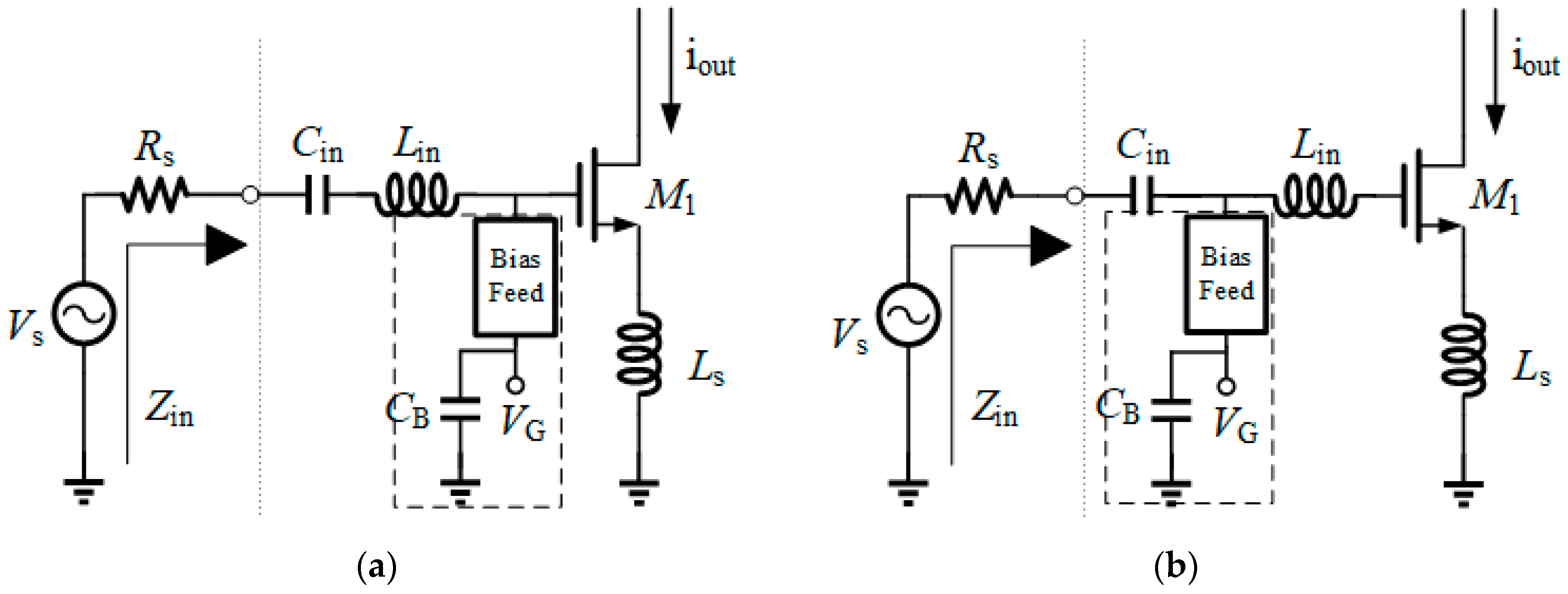
Figure 2 shows two placement modes of bias circuit with SNIM. Vs stands for the signal source who feeds RF signal and Rs is its intrinsic impedance. Capacitor Cin is used to block the DC signal and inductors Lin and Ls are introduced to get SNIM. Under ideal conditions, the blocking capacitor Cin can be neglected. The schematic diagram of input small signal of two modes can be seen in Figure 3.
According to the SNIM method, the small signal input impedance can be expressed as
Z i n = s L i n + s L s + 1 s C g s + ω T L s
where ω T = g m / C g s . In RF applications, LNA receives signals from antenna whose intrinsic impedance Rs is commonly 50 Ω. For input matching, Zin should get conjugate match with source impedance. Moreover, for noise matching, Zin should be equal to the optimum source impedance, which is set to Rs in SNIM. That is to say, as long as SNIM is achieved, Zin from Equation (1) is equal to Rs and the imaginary part is equal to 0. When taking non-ideal bias circuit into account, the input impedance can be expressed as
Z i n 1 = s L i n + Z B ( s L s + 1 s C g s + ω T L s )
Z i n 2 = Z B ( s L i n + s L s + 1 s C g s + ω T L s )
where Zin1 stands for condition of bias circuit postposition after Lin in Figure 2a and Zin2 stands for condition of bias circuit proposition before Lin in Figure 2b.
From the viewpoint of size reduction, the inductor bias-feed circuit needs an area consumptive off- or on-chip inductor and the use of an on-chip resistor bias feed instead of an inductor bias feed is preferable [21]. By this means, in Equations (2) and (3), Z B = R B . From Equation (1), the Zin is equal to 50 Ω, so Equations (2) and (3) can be simplified as
Z i n 1 = R s ( s L i n ) 2 R B s L i n
Z i n 2 = R B R s
From Equation (5), we can easily conclude Zin2 is approximately equal to Rs as long as ZB is much larger than Rs. As for Zin1, an extra inductive impedance part is added, leading to mismatch of input-matching and noise-matching.
To find a proper resistor for bias circuit, simulation of two placement modes of bias circuit with different resistors from 300 Ω to 3000 Ω is carried out and the results shown in Figure 4. To simplify the comparison, the second stage of the LNA is discarded. Three main parameters: K factor, noise figure and S11, presenting the stability, noise matching and input matching, respectively, most sensitive to bias circuit, are selected as performance index.
Researchers found proper resistance bias resistor could enhance the stability of amplifiers [22]. Unconditional stability in whole band is a must for LNA to avoid oscillation happening, which is unexpected for designers. Therefore, keeping the circuit stable is top priority, which means the K factor should be larger than 1 in the whole band. Figure 4a depicted K factor of bias circuit postposition after Lin and Figure 4b depicted K factor of bias circuit proposition before Lin. The two results share the same trend. From Figure 4a, b, the stability is decreasing with the bias resistance increasing. However, when bias resistance is larger than 1500 Ω, the K curve will show a part below 1. We commonly call this part “unstable area”. In this design, the bias resistor with resistance no more than 1500 Ω is allowed.
Figure 4c,d depicted NF with different resistance bias circuits in two conditions mentioned above. On the whole, the NF performance is better as the bias resistance is larger. With same bias resistor, results in Figure 4c show higher noise than Figure 4d. It is consistent with former theoretical derivation in Equations (4) and (5), indicating that resistor bias circuit postposition after Lin has a greater effect on SINM than resistor bias circuit proposition before Lin. Figure 4d also indicated that when bias resistance is larger than 1200 Ω, the decreasing trend of NF is not obvious. It can be assumed that resistance of bias resistor is accepted when larger than 1200 Ω. Input reflecting parameter S11 of two conditions are shown in Figure 4e,f. With bias resistance increasing, S11 performance became better. Compared with figure S11 in Figure 4e, the minimum point frequency of S11 shown in Figure 4f is more constant. In practice, S11 is adequate when it is below 10 dB. The frequency band of S11 below 10 dB in Figure 4f is wider than the one in Figure 4e. Once again, the resistor bias circuit proposition before Lin has proved to be better than resistor bias circuit postposition after Lin.
After taking K factor, NF and S11 into consideration, a 1200 Ω resistor is chosen in bias circuit to make the circuit unconditionally stable in whole band and good performance of noise figure and input reflection parameter S11.

2.1.2. Bias Points Design

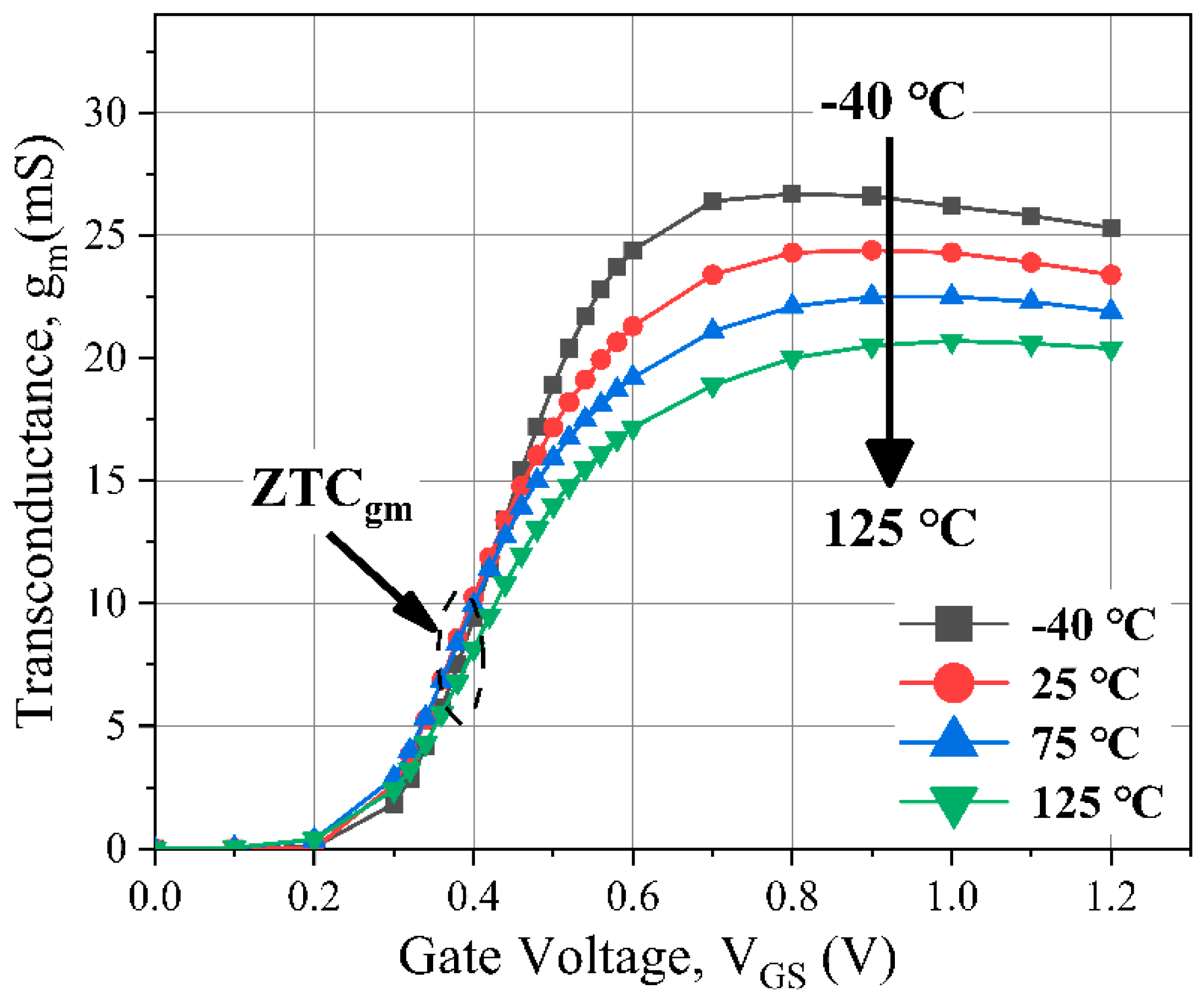
To make the circuit low-power and temperature-stable, a proper bias point is of great significance. For the CMOS technology MOSFETs, there is a particular bias point characterizing the temperature behavior called “Zero Temperature Coefficient” (ZTC) [18].The ZTC bias point is defined as the bias at which the transconductance characteristic (gm-VGS) of the MOSFET remains constant when temperature varies, as shown in Figure 5.
From Figure 5, the ZTC can be observed to be 0.4 V, which means transconductance of the MOSFET can be constant when temperature varies from −40 °C to 125 °C at the bias voltage of 0.4 V. However, the gm in ZTC, which plays an important role in gain, is not big enough to keep adequate gain performance. Based on the simulation results, variation at different temperatures of NF and power became more gently with bias voltage increasing. Setting bias voltage to 0.4 V can achieve temperature-stable gain performance, while degrading NF and power consumption consistency at different temperatures. To make the LNA a balanced one, NF, gain and power as well as their temperature variations should be taken into consideration. After simulation and comparison, bias points of amplificatory transistors are elaborately set to 0.55 V for enough gain, acceptable NF and power consumption reduction, sacrificing temperature stability to a certain extent.

2.2. Two-Stage Single-End LNA Design

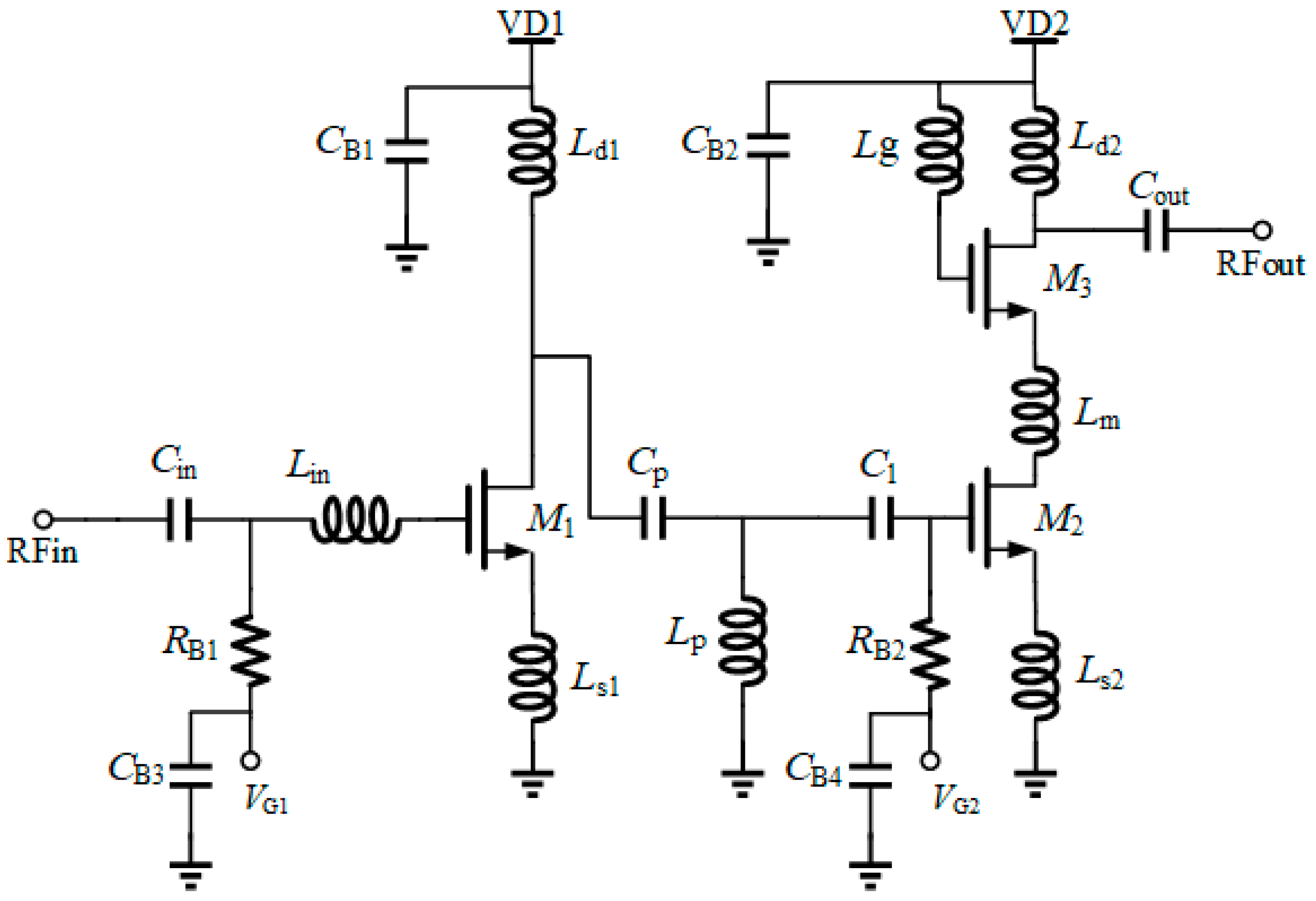
On the basis of optimized resistor bias circuit, a two-stage single-end LNA is designed in our work. The single-end topology is adopted to avert lossy balun and additional power consumption. To meet the requirements of noise figure and gain, a common-source (CS) amplifier is set to be first stage to keep the circuit low-noise, followed by a cascode amplifier to enhance gain. The schematic of proposed two-stage single-end LNA is shown in Figure 6.
As depicted in Figure 6, sizes of transistors M1, M2 and M3 are selected elaborately through simulating. Moreover, proper biasing is chosen to make the circuit keep low-noise and adequate gain. Lm, as neutralized inductor, is added between the CS and the common-gate (CG) to resonate with parasitic capacitor to minimize the NF and increase the gain [23]. Meantime, an inductor Lg is added at the gate of the CG transistor as resonant tank to boost gain at the target frequency [24]. Lm is well-designed transmission line fabricated with upmost metal to maintain high Q, as well as Lg. A matching network composed of Cp, Lp and C1 is used to get interstage match and transfer signal. CB1-CB4 are bypass capacitors for leaching the clutter signal from supply source. The elements values of proposed LNA is shown in Table 1.
To reduce the power consumption, VD1 was set to be 0.45 V while VD2 was set to be 1.2 V. The bias points of M1 and M2 were set to 0.55 V, as discussed above. Parasitic parameters of transistors was extracted with Calibre. Passive part of the layout, such as inductors, capacitors and transmission lines were simulated in ADS momentum EM simulator.

3. Results

The proposed LNA was fabricated in a 90-nm SOI CMOS process. The chip photo is shown in Figure 7. To minimize the chip area and avoid degrading performance, elements were put closely to each other based on the EM simulation results. Every DC pad had connected to ground chip with an on-chip 2 pF decoupling capacitor. Finally, a compact LNA chip size of 0.63 mm × 0.5 mm was achieved. Excluding pads and edge, the chip was only 0.47 mm × 0.33 mm. The power consumption was only 4 mW with assigned supply voltage. Compared with others [6,9,11,13,14], it consumed the least power and occupies a rather small area.
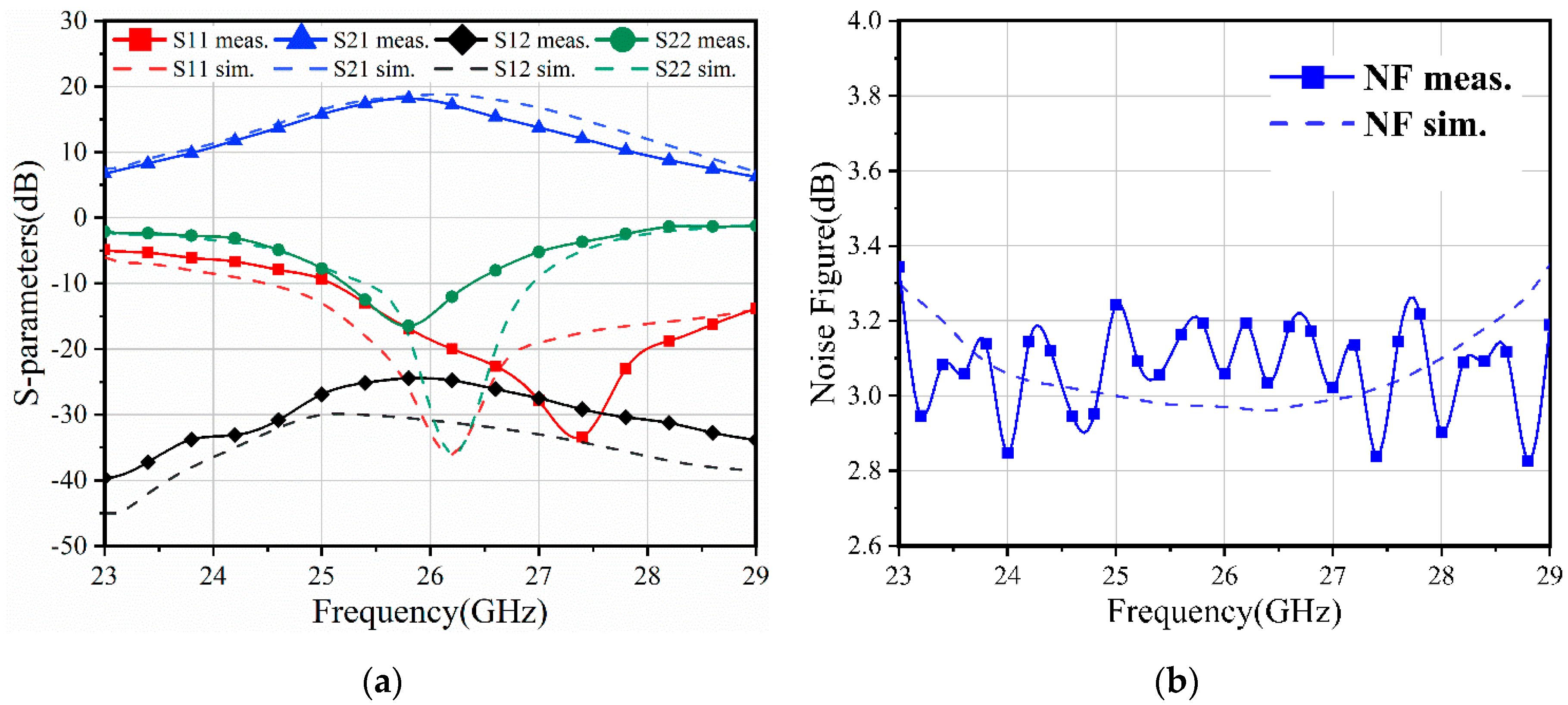
Measurements at ambient temperature of this 28 GHz LNA were carried out on an RF probe station to avoid the parasitic effects introduced by the packing, circuit board or connection wires. The Agilent N5247A network analyzer offered platform for small-signal measurements. NF was measured with Agilent N8975A NFA series noise figure analyzer. The measured and simulated small signal results are shown in Figure 8a. The measured S21 was identical to simulated S21 in the frequency band before 26 GHz. After gain reached its peak of 18.1 dB at 26 GHz, the measured S21 began to be lower than simulated one. The −3 dB bandwidth measured was about 2 GHz from 24.8 GHz to 26.8 GHz, much less than the simulated bandwidth of 3 dB from 24.5 GHz to 27.5 GHz. The reason may be the worsened S22 measured than simulated. The S11 was lower than −10 dB from 25 GHz to 29 GHz and S22 was under −10 dB from 25.2 GHz to 26.5 GHz. Moreover, S12 seen in Figure 8a showed good reverse isolation below −25 dB throughout the band. Figure 8b shows the measured and simulated NF. An average 3.1 dB noise figure (NF) in operating frequency band was obtained in this design, and the minimum NF was 2.8 dB at 24 GHz and 27.5 GHz.
Figure 9a,b illustrated IP1 dB and IIP3 separately. The power gain versus input power was plotted in Figure 9a, from which an IP1 dB of −16 dBm at 26 GHz can be extracted. The IIP3 is −6 dBm from Figure 9b. Measurement results showed poor linearity of the design. Linearity, gain and power consumption are always tradeoff. In this design, the gain and power consumption are relatively good, especially the latter. By increasing power consumption, linearity can improve a lot.
The performance of the proposed LNA is summarized in Table 2 together with the performance characterizations of other reported 28 GHz LNAs. Compared with the others, this work demonstrated the lowest power consumption and rather small area due to proper bias resistor selection and introduction of neutralized and boost inductors, making the LNA compact one.
High and low temperature semiautomatic probe station was used to measure the RF performance of LNA at different temperatures, as shown in Figure 10. To assess the temperature characteristic of the LNA, range from −40 °C to 125 °C was chosen and four representative temperatures were selected to be −40 °C, 25 °C, 75 °C and 125 °C. As can be seen, the LNA had a decreasing power gain from 18.8 dB to 15.8 dB with temperature arising, and average NF had an opposite trend from 2.3 dB to 4.2 dB. Meanwhile, power consumption varied from 3.7 mW to 4.5 mW.
Performance comparison of proposed LNA and others at different temperatures are summarized in Table 3. No one has studied performance of LNA for 5G application at different temperatures, while article [15,27] can be as reference because the performances variations share same tendency with the wide range of temperature. As can be seen, the 1.9 dB variation of NF and 0.8 dB variation of power consumption were the smallest among them. Though article [15] showed better gain-stable performance, the NF and power consumption varied much at different temperatures. After comprehensive consideration of gain, NF and power consumption variation, the proposed LNA shows good temperature stability.

4. Conclusions

In this paper, the influence of the bias circuit with SNIM is studied, which is of great significance for LNA design. Proper resistance of bias resistor can make the circuit unconditionally stable in the whole band, enhance gain and decrease NF without deteriorating the SNIM state. Bias points of the circuit were chosen to keep performance temperature-stable and reduce power consumption. Neutralized technology and boost inductors were introduced to improve performance. Based on these, a two-stage single-end LNA is fabricated in 90-nm SOI CMOS technology occupying only 0.16 mm2 core area. Experimental results showed a maximum small signal gain of 18.1 dB with 3.1 dB average NF, while consuming only four microwatts. The little variation of performance at different temperatures showed good temperature stability. These results demonstrated that the proposed LNA can be a promising candidate for 5G applications.

Author Contributions

Conceptualization, D.L.; methodology, Q.X.; software, J.H.; validation, J.L.; resources, H.C.; writing—review and editing, B.S.; project administration, H.L. All authors have read and agreed to the published version of the manuscript.

Funding

This work was supported by the National Key Research and Development Program of China under Grant No. 2016YFA0202304 and 2016YFA0201903, General Program of National Natural Science Foundation of China under Grant No.61674168 and 61504165, as well as the Opening Project of Key Laboratory of Microelectronics Devices and Integrated Technology, Institute of Microelectronics, Chinese Academy of Sciences.

Acknowledgments

The authors would like to thank Yankui Li for the measurement support.

Conflicts of Interest

The authors declare no conflicts of interest.

References

  1. Sadhu, B.; Tousi, Y.; Hallin, J.; Sahl, S.; Reynolds, S.K.; Renstrom, O.; Sjogren, K.; Haapalahti, O.; Mazor, N.; Bokinge, B.; et al. A 28-GHz 32-Element TRX Phased-Array IC with Concurrent Dual-Polarized Operation and Orthogonal Phase and Gain Control for 5G Communications. IEEE J. Solid State Circuits 2017, 52, 3373–3391. [Google Scholar] [CrossRef]
  2. Kim, H.T.; Park, B.S.; Oh, S.M.; Song, S.S.; Ho, Y.C. A 28GHz CMOS direct conversion transceiver with packaged antenna arrays for 5G cellular system. In Proceedings of the 2017 IEEE Radio Frequency Integrated Circuits Symposium (RFIC), Honolulu, HI, USA, 4–6 June 2017; pp. 69–72. [Google Scholar] [CrossRef]
  3. Kibaroglu, K.; Sayginer, M.; Phelps, T.; Rebeiz, G.M. A 64-Element 28-GHz phased-array transceiver with 52-dBm EIRP and 8–12-Gb/s 5G link at 300 meters without any calibration. IEEE Trans. Microw. Theory Tech. 2018, 66, 5796–5811. [Google Scholar] [CrossRef]
  4. Chettri, L.; Bera, R. A Comprehensive Survey on Internet of Things (IoT) Toward 5G Wireless Systems. IEEE Internet Things J. 2020, 7, 16–32. [Google Scholar] [CrossRef]
  5. Xia, Q.; Li, D.; Huang, J.; Li, J.; Chang, H.; Sun, B.; Liu, H. A 28 GHz Linear Power Amplifier Based on CPW Matching Networks with Series-Connected DC-Blocking Capacitors. Electronics 2020, 9, 617. [Google Scholar] [CrossRef] [Green Version]
  6. Elkholy, M.; Shakib, S.; Dunworth, J.; Aparin, V.; Entesari, K. A Wideband Variable Gain LNA with High OIP3 for 5G Using 40-nm Bulk CMOS. IEEE Microw. Wirel. Compon. Lett. 2018, 28, 64–66. [Google Scholar] [CrossRef]
  7. Ku, B.H.; Inac, O.; Chang, M.; Yang, H.H.; Rebeiz, G.M. A high-linearity 76–85-GHz 16-element 8-transmit/8-receive phased-array chip with high isolation and flip-chip packaging. Microw. Theory Tech. 2014, 62, 2337–2356. [Google Scholar] [CrossRef]
  8. Madan, A.; McPartlin, M.J.; Masse, C.; Vaillancourt, W.; Cressler, J.D. A 5 GHz 0.95 dB NF Highly Linear Cascode Floating-Body LNA in 180 nm SOI CMOS Technology. IEEE Microw. Wirel. Compon. Lett. 2012, 22, 200–202. [Google Scholar] [CrossRef]
  9. Ahn, H.J.; Chang, W.I.; Kim, S.M.; Park, B.J.; Yook, J.-M.; Eo, Y.-S. 28 GHz GaAs pHEMT MMICs and RF front-end module for 5G communication systems. Microw. Opt. Technol. Lett. 2019, 61, 878–882. [Google Scholar] [CrossRef]
  10. Chen, C.-C.; Lin, Y.-S.; Huang, G.-W.; Lu, S.-S. A 5.79-dB NF, 30-GHz-band monolithic LNA with 10 mW power consumption in standard 0.18-μm CMOS technology. Microw. Opt. Technol. Lett. 2009, 51, 933–937. [Google Scholar] [CrossRef]
  11. Luo, J.; He, J.; Wang, H.; Chang, S.; Huang, Q.; Yu, X.-P. A 28 GHz LNA using defected ground structure for 5G application. Microw. Opt. Technol. Lett. 2018, 60, 1067–1072. [Google Scholar] [CrossRef]
  12. Li, C.; El-Aassar, O.; Kumar, A.; Boenke, M.; Rebeiz, G.M. LNA Design with CMOS SOI Process-l.4dB NF K/Ka band LNA. In Proceedings of the 2018 IEEE/MTT-S International Microwave Symposium—IMS, Philadelphia, PA, USA, 10–15 June 2018; pp. 1484–1486. [Google Scholar] [CrossRef]
  13. Zhang, C.; Zhang, F.; Syed, S.; Otto, M.; Bellaouar, A. A Low Noise Figure 28GHz LNA in 22nm FDSOI Technology. In Proceedings of the 2019 IEEE Radio Frequency Integrated Circuits Symposium (RFIC), Boston, MA, USA, 2–4 June 2019; pp. 207–210. [Google Scholar] [CrossRef]
  14. Issakov, V.; Ciocoveanu, R. Low-Power K-Band LNA in 45 nm SOI CMOS. In Proceedings of the 2019 IEEE International Conference on Microwaves, Antennas, Communications and Electronic Systems (COMCAS), Tel-Aviv, Israel, 4–6 November 2019; pp. 1–4. [Google Scholar] [CrossRef]
  15. El Kaamouchi, M.; Moussa, M.S.; Raskin, J.-P.; Vanhoenacker-Janvier, D. Zero-temperature-coefficient biasing point of 2.4-GHz LNA in PD SOI CMOS technology. In Proceedings of the 2007 European Microwave Conference, Munich, Germany, 9–12 October 2007; pp. 1101–1104. [Google Scholar] [CrossRef]
  16. Taniguchi, E.; Ikushima, T.; Itoh, K.; Suematsu, N. A dual bias-feed circuit design for SiGe HBT low-noise linear amplifier. IEEE Trans. Microw. Theory Tech. 2003, 51, 414–421. [Google Scholar] [CrossRef]
  17. Dickson, T.; Yau, K.; Chalvatzis, T.; Mangan, A.; Laskin, E.; Beerkens, R.; Westergaard, P.; Tazlauanu, M.; Yang, M.-T.; Voinigescu, S. The Invariance of Characteristic Current Densities in Nanoscale MOSFETs and Its Impact on Algorithmic Design Methodologies and Design Porting of Si(Ge) (Bi)CMOS High-Speed Building Blocks. IEEE J. Solid State Circuits 2006, 41, 1830–1845. [Google Scholar] [CrossRef]
  18. Chen, W.-L.; Chang, S.-F.; Chen, K.-M.; Huang, G.-W.; Chang, J.-C. Temperature Effect on Kυ-Band Current-Reused Common-Gate LNA in 0.13-μm CMOS Technology. IEEE Trans. Microw. Theory Tech. 2009, 57, 2131–2138. [Google Scholar] [CrossRef]
  19. Osman, A.; Osman, M.; Dogan, N.; Imam, M. Zero-temperature-coefficient biasing point of partially depleted SOI MOSFET’s. IEEE Trans. Electron Devices 1995, 42, 1709–1711. [Google Scholar] [CrossRef]
  20. Nguyen, T.-K.; Kim, C.-H.; Ihm, G.-J.; Yang, M.-S.; Lee, S.-G. CMOS Low-Noise Amplifier Design Optimization Techniques. IEEE Trans. Microw. Theory Tech. 2004, 52, 1433–1442. [Google Scholar] [CrossRef]
  21. Soyuer, M.; Plouchart, J.-O.; Ainspan, H.; Burghartz, J. A 5.8-GHz 1-V low-noise amplifier in SiGe bipolar technology. In Proceedings of the 1997 IEEE Radio Frequency Integrated Circuits (RFIC) Symposium. Digest of Technical Papers, Denver, CO, USA, 10 June 1997; pp. 19–22. [Google Scholar] [CrossRef]
  22. Tsay, J.; Lopez, J.; Lie, D. The impacts of base bias resistor and LTE 16QAM signal bandwidth on high-efficiency linear SiGe power amplifier design. In Proceedings of the 2016 IEEE Bipolar/BiCMOS Circuits and Technology Meeting (BCTM), New Brunswick, NJ, USA, 25–27 September 2016; pp. 52–55. [Google Scholar] [CrossRef]
  23. Huang, B.-J.; Lin, K.-Y.; Wang, H. Millimeter-Wave Low Power and Miniature CMOS Multicascode Low-Noise Amplifiers with Noise Reduction Topology. IEEE Trans. Microw. Theory Tech. 2009, 57, 3049–3059. [Google Scholar] [CrossRef]
  24. Yu, Z.; Feng, J.; Guo, Y.; Li, Z. Analysis and design of a V-band low-noise amplifier in 90 nm CMOS for 60 GHz applications. IEICE Electron. Express 2015, 12. [Google Scholar] [CrossRef] [Green Version]
  25. Kodak, U.; Rebeiz, G.M. A 42mW 26–28 GHz phased-array receive channel with 12 dB gain, 4 dB NF and 0 dBm IIP3 in 45nm CMOS SOI. In Proceedings of the 2016 IEEE Radio Frequency Integrated Circuits Symposium (RFIC), San Francisco, CA, USA, 22–24 May 2016; pp. 348–351. [Google Scholar] [CrossRef]
  26. Cui, B.; Long, J.R.; Harame, D.L. A 1.7-dB Minimum NF, 22-32 GHz Low-Noise Feedback Amplifier with Multistage Noise Matching in 22-nm SOI-CMOS. In Proceedings of the 2019 IEEE Radio Frequency Integrated Circuits Symposium (RFIC), Boston, MA, USA, 2–4 June 2019; pp. 211–214. [Google Scholar] [CrossRef]
  27. Zhao, C.; Kang, K. A Ku-band Miniaturized LNA in 0.18-µm CMOS Process for Low-cost Phased Array Application. In Proceedings of the 2019 IEEE International Symposium on Radio-Frequency Integration Technology (RFIT), Nanjing, China, 28–30 August 2019; pp. 1–3. [Google Scholar] [CrossRef]
Figure 1. Block diagram of the phased-array transceiver.
Electronics 09 01225 g001
Figure 2. (a) Input schematic diagram with bias circuit postposition after Lin; (b) input schematic diagram with bias circuit proposition before Lin.
Electronics 09 01225 g002
Figure 3. Schematic diagram of input small signal.
Electronics 09 01225 g003
Figure 4. (a) Simulated K factor with resistor bias circuit postposition after Lin; (b) simulated K factor with resistor bias circuit proposition before Lin; (c) simulated noise figure with resistor bias circuit postposition after Lin; (d) simulated noise figure with resistor bias circuit proposition before Lin; (e) simulated S11 with resistor bias circuit postposition after Lin; (f) simulated S11 with resistor bias circuit proposition before Lin.
Electronics 09 01225 g004
Figure 5. Simulated gm vs. VGS at different temperatures.
Electronics 09 01225 g005
Figure 6. Schematic of two-stage single-end low-noise amplifier (LNA).
Electronics 09 01225 g006
Figure 7. Chip photo of the proposed LNA.
Electronics 09 01225 g007
Figure 8. (a) S-parameters of measurements and simulations; (b) noise figure of measurements and simulations.
Electronics 09 01225 g008
Figure 9. (a) P1dB of proposed LNA; (b) IIP3 of proposed LNA.
Electronics 09 01225 g009
Figure 10. (a) Measured S21 at different temperatures; (b) measured NF at different temperatures.
Electronics 09 01225 g010
Table 1. Elements values of proposed LNA.
M1–M3Cin/CoutCB1-CB4RB1/RB2CpC1Lin
30 um/90 nm1.25 pF2 pF1.2 kΩ110 fF1 pF680 pH
Ls1Ls2Ld1Ld2LmLg
300 pH270 pH550 pH700 pH140 pH160 pH
Table 2. Performance comparison table.
This Work[13][14][25][26][12]
Technology90 nm SOI22 nm SOI45 nm SOI45 nm SOI22 nm SOI45 nm SOI
Topology 12 SE1 SE1 SE1 SE2 SE1 SE
Bias circuitresistiveoff-chipresistiveinductiveoff-chipresistive
Gain (dB)18.112.610.58.520.112.8
NF 2 (dB)3.11.351.631.951.4
IP1 dB (dBm)–16–7.9–10.33.5NANA
IIP3 (dBm)–61.4NANA−145
PDC (mW)41361217.37
Area 3 (mm2)0.160.210.18NA0.050.3
1: “2 SE” refers to 2-stage single-end; “3 Diff.” refers to 3-stage differential; 2: average NF; 3: core area without pads.
Table 3. Performance comparison table at different temperatures.
This Work[15][27]
Technology90 nm SOI CMOS130 nm SOI CMOS180 nm CMOS
Frequency (GHz)262.517
Gain (dB)15.8–18.89.1–1018.7–23
Gain variation (dB)30.94.3
NF (dB)2.3–4.23.4–5.72.2–4.3
NF variation (dB)1.92.32.1
Power consumption (mW)3.7–4.52.2–3.766 1
Power variation (mW)0.81.5NA
Temperature range (°C)−40–12525–200−55–120
1: power consumption at ambient temperature.