Abstract
This paper presents a novel topology of a modified isolated single-ended-primary-inductance converter (SEPIC) with a model predictive control (MPC) approach applied to direct current (DC) electronic loads. The proposed converter uses an actual transformer rather than a coupled inductor for isolation between the source and the load. The transformer allows the proposed converter to operate at a higher switching frequency, ultimately reducing the passive components’ size. A low-power hardware prototype is developed and tested with a model predictive control algorithm under variable input voltages and load conditions. The performance of the proposed converter is demonstrated to be satisfactory under steady state, as well as sudden input voltage transients. The proposed converter utilizes a switched capacitor technique to generate alternating current in both windings of the transformer. As the coupled inductor is eliminated from the circuit, the problem of high voltage spikes occurring due to leakage inductances is also eliminated for the proposed converter. Therefore, the proposed converter can be used for isolated medium power applications. The experimental results show that the efficiency of the proposed converter reached 96%. The MPC allows this converter’s DC voltage level to remain stable even as the input voltage and output terminal load change. Lastly, this converter with an MPC approach can be applied to different DC electronic loads, improving DC power quality and DC electronic load life.
Keywords:
DC/DC converter; high-frequency transformer; electrical isolation; model predictive control MSC:
93B52; 94C11; 93B45
1. Introduction
The need for electricity is increasing day by day, and thus, researchers are focusing on methods to produce electricity by utilizing renewable energy sources. However, depending on environmental factors, this renewable energy is only accessible for a specific period of time at a specific location [1,2,3]. For example, solar energy is only accessible during the daytime; therefore, we must store this energy to use whenever required in the absence of solar radiation, and thus most batteries are typically used for this purpose [4]. These batteries require a direct current (DC) power source for charging, and similarly, it acts as a DC power source whenever required. Therefore, researchers are working to upgrade these DC-DC converters to isolated boost circuits so that we can have efficient and affordable power electronic converters under all operating situations that are essential for isolated power supply [5,6].
Initially, we had conventional DC-DC converters including buck, boost, buck-boost, zeta, cuk, and single-ended-primary-inductance converter (SEPIC). Each of these converters has its advantages and drawbacks in terms of cost, the complexity of the controller, and efficiency. These could only vary the output voltage and had the disadvantage of not having electrical isolation between the input power source and output load. Later isolated converters, such as the flyback, LLC resonant converter, and push-pull, were introduced. The simplest isolated converter is the flyback converter. It has only one power switch but uses a coupled inductor as a means of an energy storage element. The converters which are using coupled inductors are incapable of handling high power because of the leakage inductance of the coupled inductor [7,8,9]. Sometimes electrical isolation is mandatory between the electrical source and the load to protect the device or the working person [10,11,12,13,14].
In most applications, we need to control the output voltage or current of these converters depending on the applications. For controlling these parameters various control techniques were used, the simplest one is the proportional-integral (PI) control, but it requires a linear system to be controlled and it is not applicable to the non-linear systems. To improve the system’s dynamic response, control objectives and nonlinear control strategies are introduced for DC-DC converters [15]. For example, model predictive control (MPC) and sliding mode control (SMC) are notable for their quick dynamic response and robustness [16]. The model predictive control is an optimal control strategy in which the system’s current state is used to determine the solution of the finite-horizon optimal control problem at each sampling instance. The regulating speed of MPC is quicker than the proportional-integral and derivative (PID) as it repeatedly runs the online calculation of optimization and applies the suitable control signal to the system where it can smoothly resist the effects of disturbances. The MPC has been applied to the field of power electronics with precise mathematical models [17], including three-phase DC-alternating current (AC) and AC-DC systems, as well as DC-DC converters [18,19,20,21,22].
Many single-switch isolated converters are available in the literature, but most are incapable of dealing with high power. The simplest isolated converter is the flyback converter but uses a coupled inductor for isolation instead of a transformer. In the case of coupled inductors, the leakage inductance is quite high because of the air gap in their core. When the switch is turned off the current for this leakage inductor becomes zero instantly and a high voltage spike is developed in the circuit due to Lk(diLk/dt). As the output power increases the magnitude of this generated voltage spike also increases which may damage the other components of the circuit, especially the power switch. To overcome the issue of high voltage spikes due to leakage inductance, we have developed a modified isolated SEPIC converter as explained in the next sections.
The conventional isolated single-ended-primary-inductance converter (SEPIC) is shown in Figure 1, and the voltage gain is given by Equation (1) as explained in [23]. The current in the primary winding N1 is AC, but the current in the secondary winding N2 is DC because of the output diode D1. Therefore, we need a coupled inductor to hold the energy in its air gap for the duration of when the power is not transferring to the load from the primary side to the output load, which is when the output diode is not conducting. Because of this air gap, there is a series connected leakage inductance, as shown in Figure 1, which is responsible for the high voltage spikes in the circuit.
where:
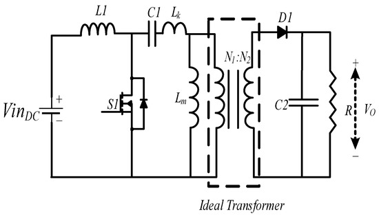
Figure 1.
Conventional isolated SEPIC converter.
- is the output voltage of the converter.
- is the input voltage of the converter.
- is the number of turns on the primary side of the coupled inductor.
- is the number of turns on the secondary side of the coupled inductor.
- is the duty ratio of the pulse-width modulation (PWM) gating signal.
Suppose we can create alternating currents in both windings with a zero-phase difference, and then, we can replace this coupled inductor with a transformer with negligible leakage inductance, which solves the problem of voltage spikes. This can be performed by adding an extra diode and a capacitor at the secondary side as shown in Figure 2, and this is the proposed modified isolated SEPIC converter.
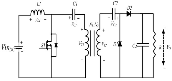
Figure 2.
Proposed isolated SEPIC converter.
The main features of the proposed modified SEPIC converter are as follows:
- The proposed converter fundamentally evolved from the conventional isolated SEPIC converter by employing the transformer and a few auxiliary components to boost the gain of the converter.
- Transformer provides electrical isolation between the input and the electrical load.
- This converter is appropriate for medium power applications as it uses a real transformer rather than a coupled inductor.
- The proposed converter is cost-effective as it uses only one switch for its operation and control.
2. Working of Proposed Converter in CCM and DCM Mode of Operation
When the switch is turned on, the diode D2 gets reversed biased as shown in Figure 3. The related Kirchhoff’s voltage law (KVL) equations for the switched-on mode of operation are as follows:
where:
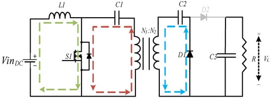
Figure 3.
Equivalent circuit for the switch-on mode of operation.
- is inductor voltage.
- is the voltage across capacitor C1.
- is the voltage across capacitor C2.
- is the primary side voltage of the transformer.
- is the secondary side voltage of the transformer.
For the second mode of operation when the switch is off, the diode D2 starts conducting and D1 is reversed biased, as shown in Figure 4. The KVL equations for the switched-off mode of operation are as follows:
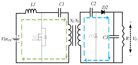
Figure 4.
Equivalent circuit for the switch-off mode of operation.
After applying a volt-second balance across the inductor, the voltage gain equation is obtained as Equation (12). The voltage gain equation is similar to that of the conventional boost converter with the benefits of the transformer.
The voltage stress across the switch is given by Equation (13) and it is independent of the turn ratio, which is at higher values of the turn ratio, the output voltage increases but the voltage stress across the switch remains the same.
where:
- is switch voltage when it is not conducting.
The size of the passive components can be calculated by using the following equations.
where:
- is the converter input power.
- is the converter output power.
- is the inductor average current.
- is the required inductance of the inductor.
- is the switching frequency.
- is the permissible ripple in the capacitor voltage.
- is the required capacitance.
The choice of the capacitor depends on a maximum allowable voltage ripple as well as a voltage across the capacitor itself. While making the selection of the capacitor and preventing it from bursting, its value should be high enough to sustain it from the high voltage that may be applied across it.
For the proposed modified isolated SEPIC converter, the normalized inductor time constant is defined by Equation (24), and the boundary time constant for continuous conduction mode (CCM) and discontinuous conduction mode (DCM) is defined by Equation (25). For continuous conduction mode , otherwise, the circuit enters the discontinuous mode of operation. The boundary conditions for CCM and DCM are shown in Figure 5, with a transformer of unity turn ratio; Equation (25) is used to draw this curve. In the case of DCM, there are three modes of operation, as shown in Figure 6.
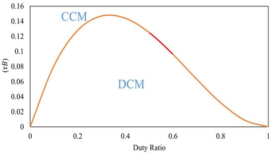
Figure 5.
Boundary conditions for CCM and DCM mode of operation.
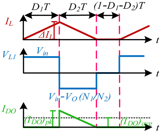
Figure 6.
Waveforms in DCM.
The first two modes are the same as that of the CCM and in the third mode the current in the inductors becomes zero as shown in the Figure 6; therefore, the voltage gain for the DCM can be calculated by applying volt–second across the inductors as follows:
The average output current is always equal to the average current of the output diode, that is:
After solving Equations (26) and (31), we can calculate the output voltage gain for DCM, as shown by Equation (33).
3. Implementation of Model Predictive Control
Model predictive control (MPC) is a powerful control technique that can provide superior performance, greater control, and splendid accuracy over traditional methods such as PID, sliding mode control (SMC), and feedforward control which makes it an attractive option for power electronics converter control. When compared to conventional control approaches, MPC updates the system model frequently based on data collected in real time, making it more successful at managing model uncertainties. In a proposed converter, MPC can incorporate these constraints directly into the control design and ensure that they are satisfied throughout the control process. Figure 2 shows the circuit of a proposed modified isolated DC-DC SEPIC converter. It is possible to write the differential equation as in [24] by combining Equations (2) and (9) and adding the inductor ESR R1 drop and defining a switching function S to obtain the dynamic model of the input inductor current. In the finite control set model predictive control (FCS-MPC), the controlled variable is taken as the state of an energy storing element, which in our system is the input inductor current iL1.
By applying Euler’s forward approximation technique, the discrete-time derivative of iL1 can be approximated as follows:
The potential value of at the (k + 1) th sampling instant can be calculated by using Equations (34) and (35), as given by Equation (36).
In Equation (36), is the sampling period, S stands for the switching state with 1 for the on state of power MOSFET and 0 for the off state of power MOSFET, is the inductance, and is the resistance of the inductor. The preferred MPC scheme is shown in Figure 7.
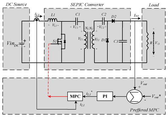
Figure 7.
Preferred model predictive control approach.
The main approach of the MPC seeks to reduce the error between the reference and predicted values. The following cost function can be used to determine the present error in the subsequent sampling interval. The basic goal of the MPC approach, as previously stated, is to identify the best feasible control action at each sampling time for all potential switching states to minimize the cost function in (37). The flowchart of the control algorithm is presented in Figure 8.
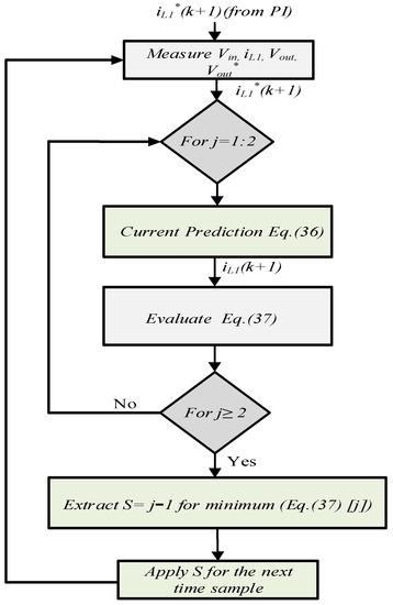
Figure 8.
Flowchart of the proposed MPC.
4. Performance Comparison
The advantage of using this proposed converter is that it provides electrical isolation between the input power source and the load, and because of this electrical isolation, it can be used for most charging applications. With the aid of the modified isolated SEPIC converter, we will obtain an output voltage that is not inverted and the same as that of a conventional boost converter with the benefit of the transformer ratio.
Table 1 refers to the comparison of the proposed isolated SEPIC converter and their advantages with some other recently developed isolated and non-isolated converter topologies in [25,26,27,28,29,30,31,32] relating to voltage gain, components required, and the voltage stress across the power switches. This proposed converter uses fewer components than the converter presented in [26,27,28,29,30,31,32] which reduces the cost of the converter when employed in practical applications. Table 2 illustrates the comparison among the preferred MPC approach with DC-DC buck [16,33], DC-DC boost [34,35], and DC-DC SEPIC MPC [36] converters. In addition, the comparison includes the indirect SMC approach developed for DC-DC SEPIC converters [24]. The preferred MPC approach is compared to these six control methods on different parameters as shown in Table 2, and it is apparent that the preferred MPC approach is more preferable to the other alternatives in terms of control, robustness, and complexity (because it does not require any filter). It also has a negligible effect on parameter variation and has a moderate settling time with zero steady-state error in the output voltage.

Table 1.
This comparison of modified isolated-SEPIC converter with existing isolated and non-isolated topologies.
Table 2.
Comparison of six control methods with the implemented control technique.
5. Simulation Results
The simulation results are carried out using the MATLAB R2021b software to test the efficacy of the proposed modified isolated SEPIC converter. As illustrated in Figure 9a, the measured output voltage is determined to be 38 V at an input voltage of 24 V, with a duty ratio of 0.4. Figure 9b shows the output current of the proposed converter. The modest voltage loss is caused due to parasitic and on state resistances of the converter. Figure 9d and Figure 9e display the capacitor voltage of C1 and C2, and it is found to be 24 V and 23 V, respectively. These values are in conformity with the theoretical study. The inductor current is continuous, and the average value of is determined to be 0.8 A, as shown in Figure 9f. Figure 10a shows the simulation results of the preferred MPC against rapid RL change from 100 Ω to 200 Ω, and Figure 10b shows the simulation waveforms of the preferred MPC with input voltage variations from 24 V to 30 V. Table 3 shows the simulation design parameters of the proposed modified isolated SEPIC converter.
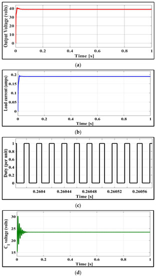
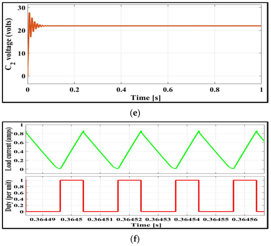
Figure 9.
Simulation results of the proposed modified isolated SEPIC converter at duty ratio of 0.4: (a) Load voltage Vo waveform; (b) Load current Io waveform; (c) PWM signal; (d) C1 voltage VC1 waveform; (e) C2 voltage VC2 waveform; (f) Inductor (L1) current iL1 waveform.
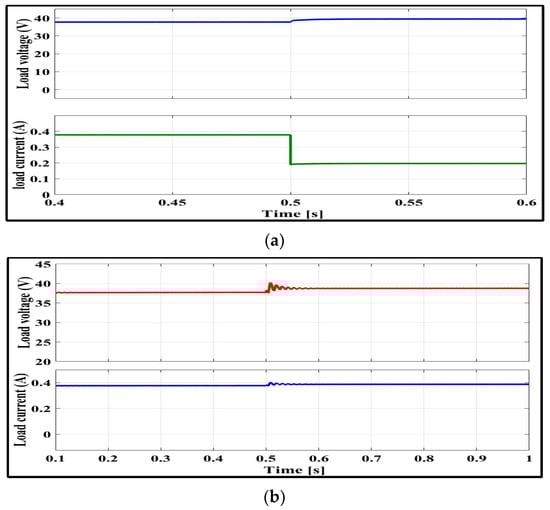
Figure 10.
Simulation Vo and Io waveforms of the preferred MPC with (a) Rapid RL change from 100 Ω to 200 Ω; (b) Input voltage variation from 24 V to 30 V.
Table 3.
Simulation design parameter.
6. Hardware Results
To validate the theoretical aspects of the proposed modified isolated SEPIC converter, a low-power hardware prototype is developed and tested under laboratory conditions. The experimental parameters are given in Table 4, and the developed hardware prototype is shown in Figure 11.
Table 4.
Comparison design parameter.
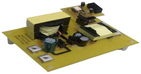
Figure 11.
Developed hardware prototype.
To test the hardware, a PWM pulse of a required duty ratio is generated through the microcontroller STM32 (Nucleo-H743ZI2). To test the circuit in the open loop, a PWM pulse is applied to the specified pin of the converter’s gate driver circuit, which operates at a duty ratio of 0.6, at a frequency of 100 kHz, and with a load resistance of 250 Ω. The switching frequency is set to 100 kHz so that the size of the passive components is reduced. The measured output voltage is 67 V, almost the same as the theoretically calculated value at an input voltage of 28 V with a duty ratio of 0.6, as depicted in Figure 12a. The converter is working in CCM, as depicted in Figure 12b. The magnitude of the voltage across both capacitors (C1 and C2) is 27 V; this is because of the unity turn ratio of the transformer.
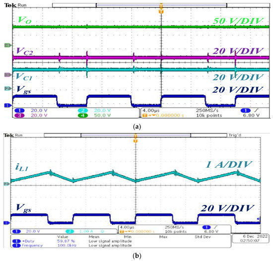
Figure 12.
Experimental results of proposed modified isolated SEPIC converter at duty ratio of 0.6: (a) Gate-source voltage Vgs, output voltage Vo, C1 voltage VC1, C2 voltage VC2 waveforms; (b) Inductor current iL1 waveform.
The results at a duty ratio of 0.4 and 0.5 with a load resistance of 50 Ω are shown in Figure 13a and Figure 13b, respectively. The measured output voltage at the 0.4 duty ratio is 36 V and 44 V at the duty ratio of 0.5 with an input voltage of 24 V. There is some deviation in the measured and theoretically calculated value, and it is because of the internal power losses of the circuit, such a switching, inductor, and capacitor resistive power losses.
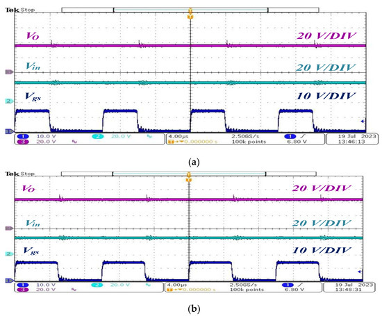
Figure 13.
Experimental results of the proposed modified isolated SEPIC converter with a load resistance of 50 Ω: (a) Vo, Vin, and Vgs waveforms at a duty ratio of 0.4; (b) Vo, Vin, and Vgs waveforms at a duty ratio of 0.5.
To test the MPC resistor, a divider-based voltage sensor is used to measure and calculate the amount of DC output voltage, and the (ACS-712) current sensor is used to sense the input current of the converter. The microcontroller then creates the control signal and applies it to the power MOSFET (C3M0060065K) gate driver. The hardware results of the modified isolated SEPIC converter with the MPC technique against rapid fluctuation in RL load are shown in Figure 14. The output voltage is the same as that of the reference voltage of 48 V, and this voltage is fixed and not changing even after changing the load by 50%.
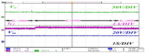
Figure 14.
Dynamic responses of preferred modified isolated SEPIC with MPC against rapid RL change and test Vo, Vin, iL1 waveforms.
Figure 15 shows the dynamic response of Vo, Vin, and iL1 for shifting the input voltage from 20 V to 24 V and from 30 V to 24 V. The responses obtained in Figure 15a show the hardware results when the Vin is switched from 20 V to 24 V; despite a short transition period, the output voltage is regulated at its reference value of 50 V. Similarly, Figure 15b shows the hardware results when Vin is shifted from 30 V to 24 V and the converter’s operation mode is changed from buck to boost mode; the output voltage is regulated at a reference of 50 V. These results demonstrate that the preferred MPC strategy regulates Vo when the input voltage varies. The proposed modified isolated SEPIC converter has a efficiency of 92.5% to 96.3% as illustrated in Figure 16.
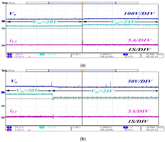
Figure 15.
Dynamic responses captured waveforms of Vo, Vin, and iL1 of preferred MPC with (a) Input voltage variation from 20 V to 24 V; (b) Input voltage variation from 30 V to 24 V.
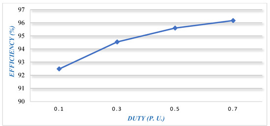
Figure 16.
Efficiency characteristics curve.
7. Conclusions
In this study, the model predictive control (MPC) is combined with the proposed converter, where it enhances DC power quality and extends the life of the DC electronic loads by providing stable output voltage levels. The design and control of the proposed modified isolated converter are simple and not as complex as in the case of resonant converters. This converter can be used for low to high-power applications as it uses a transformer rather than a coupled inductor. A multi-winding transformer can be used instead of two-winding transformers to provide multiple isolated outputs. The proposed modified isolated SEPIC converter is suitable for most charging applications as it provides electrical isolation between the source and the load.
Additionally, this proposed converter has the advantage of providing electrical isolation between the input power source and the load, which makes it suitable for most charging applications. With the aid of the modified isolated SEPIC converter, we obtain an output voltage that is not inverted and the same as that of a conventional boost converter with the benefits of transformer turn ratio. The proposed converter has a very good efficiency of more than 96% and the preferred MPC approach is more desirable than the other alternatives in terms of control, robustness, and complexity.
Furthermore, the proposed converter can be applied to renewable energy systems due to its high efficiency and isolation function, and because of these benefits, it can be used in a variety of applications. The proposed converter blends with different control mechanisms to find a more suitable control approach, so that the power system has excellent stability.
8. Future Work
There are several topologies and methodologies that have been suggested by power electronic researchers in the past [37,38,39,40], but each time they employed low band-gap switching devices that produced a significant quantity of heat when operated at high frequencies. Due to this issue, the user is forced to utilize these devices at lower frequencies, and at lower frequencies, the size of the passive components substantially rises which raises the total size, weight, and cost of the converters. To overcome this issue now, researchers are moving towards wide band-gap switching devices (SiC and GaN). These wide band-gap devices provide the facility of very high-frequency switching with very little switching power loss reducing the size of the passive components present in the circuit and improving the efficiency of the overall system. Presently wide band-gap switching device technology is mature enough and we can combine this technology with the proposed converter. An active PFC-based rectifier can be designed just by adding a full bridge diode rectifier just before the modified isolated SEPIC converter. The same conventional PFC algorithm can be used as we are using in the case of the conventional boost converter. Wireless chargers can be developed just by replacing the transformer of the modified isolated SEPIC converter with two mutually coupled induction windings.
Author Contributions
Conceptualization, M.S.K., C.-H.L. and J.A.; formal analysis, M.S.K., C.-H.L., J.A. and M.F.; investigation, M.S.K., C.-H.L. and M.F.; software, M.S.K. and J.A.; methodology, M.S.K., C.-H.L. and J.A.; data curation, M.S.K., J.A. and M.F.; visualization: M.S.K. and J.A.; funding acquisition, C.-H.L.; supervision, C.-H.L.; writing—original draft, M.S.K., C.-H.L., J.A. and H.-D.L.; writing—review and editing, M.S.K., C.-H.L., J.A. and H.-D.L. All authors have read and agreed to the published version of the manuscript.
Funding
This research was funded by the Industry-University Cooperation Project of NTUST, grant number: 10343.
Data Availability Statement
Not applicable.
Conflicts of Interest
The authors declare no conflict of interest.
References
- Elavarasan, R.M.; Shafiullah, G.M.; Padmanaban, S.; Kumar, N.M.; Annam, A.; Vetrichelvan, A.M.; Mihet-Popa, L.; Holm-Nielsen, J.B. A Comprehensive Review on Renewable Energy Development, Challenges, and Policies of Leading Indian States with an International Perspective. IEEE Access 2020, 8, 74432–74457. [Google Scholar] [CrossRef]
- Colak, A.; Ahmed, K. A Brief Review on Capacity Sizing, Control and Energy Management in Hybrid Renewable Energy Systems. In Proceedings of the 2021 10th International Conference on Renewable Energy Research and Application (ICRERA), Istanbul, Turkey, 26–29 September 2021; pp. 453–458. [Google Scholar] [CrossRef]
- Qazi, A.; Hussain, F.; Rahim, N.A.; Hardaker, G.; Alghazzawi, D.; Shaban, K.; Haruna, K. Towards Sustainable Energy: A Systematic Review of Renewable Energy Sources, Technologies, and Public Opinions. IEEE Access 2019, 7, 63837–63851. [Google Scholar] [CrossRef]
- Strasser, T.; Andren, F.; Kathan, J.; Cecati, C.; Buccella, C.; Siano, P.; Leitao, P.; Zhabelova, G.; Vyatkin, V.; Vrba, P.; et al. A Review of Architectures and Concepts for Intelligence in Future Electric Energy Systems. IEEE Trans. Ind. Electron. 2015, 62, 2424–2438. [Google Scholar] [CrossRef]
- Pachauri, N.; Thangavel, V.; Suresh, V.; Kantipudi, M.P.; Kotb, H.; Tripathi, R.N.; Bajaj, M. A Robust Fractional-Order Control Scheme for PV-Penetrated Grid-Connected Microgrid. Mathematics 2023, 11, 1283. [Google Scholar] [CrossRef]
- Liu, X.; Yu, S.S.; Zhang, G.; Lin, W.; Liu, T.; Le, W. Design and Experimental Verification of a General Single-Switch N-Stage Z-Network High Gain Boost Converter. Mathematics 2022, 10, 4758. [Google Scholar] [CrossRef]
- Hu, D.; Yin, A.; Ghaderi, D. A transformer-less single-switch boost converter with high-voltage gain and mitigated-voltage stress applicable for photovoltaic utilizations. Int. Trans. Electr. Energy Syst. 2020, 30, 1–22. [Google Scholar] [CrossRef]
- Barry, B.C.; Hayes, J.G.; Rylko, M.S. CCM and DCM operation of the interleaved two-phase boost converter with discrete and coupled inductors. IEEE Trans. Power Electron. 2015, 30, 6551–6567. [Google Scholar] [CrossRef]
- Aquino, R.N.A.L.E.S.; Tofoli, F.L.; Praca, P.P.; de Souza Oliveira, D.; Barreto, L.H.S.C., Jr. Soft switching high-voltage gain DC–DC interleaved boost converter. IET Power Electron. 2015, 8, 120–129. [Google Scholar] [CrossRef]
- Forouzesh, Y.P.; Siwakoti, S.A.; Gorji, F.; Blaabjerg, F.; Lehman, B. Step-up DC–DC converters: A comprehensive review of voltage-boosting techniques, topologies, and applications. IEEE Trans. Power Electron. 2017, 32, 9143–9178. [Google Scholar] [CrossRef]
- Miao, S.; Wang, F.; Ma, X. A new transformerless buck-boost converter with positive output voltage. IEEE Trans. Ind. Electron. 2016, 63, 2965–2975. [Google Scholar] [CrossRef]
- Meinagh, F.A.A.; Meinagh, A.; Yuan, J.; Yang, Y. New high voltage gain DC–DC converter based on modified quasi-Z-source network. In Proceedings of the IEEE 13th International Conference on Compatibility, Power Electronics and Power Engineering (CPE-POWERENG), Sonderborg, Denmark, 23–25 April 2019; pp. 1–6. [Google Scholar] [CrossRef]
- Ahmad, J.; Zaid, M.; Sarwar, A.; Lin, C.-H.; Asim, M.; Yadav, R.K.; Tariq, M.; Satpathi, K.; Alamri, B. A New High-Gain DC-DC Converter with Continuous Input Current for DC Microgrid Applications. Energies 2021, 14, 2629. [Google Scholar] [CrossRef]
- Ahmad, J.; Zaid, M.; Sarwar, A.; Tariq, M.; Sarwer, Z. A New Transformerless Quadratic Boost Converter with High Voltage Gain. Smart Sci. 2020, 8, 163–183. [Google Scholar] [CrossRef]
- Li, Z.; Li, M.; Zhao, Y.; Wang, Z.; Yu, D.; Xu, R. An Optimized Control Method of Soft-Switching and No Backflow Power for LLC Resonant-Type Dual-Active-Bridge DC-DC Converters. Mathematics 2023, 11, 287. [Google Scholar] [CrossRef]
- Ławryńczuk, M. Special Issue. Model Predictive Control: Algorithms and Applications: Foreword by the Guest Editor. Algorithms 2022, 15, 452. [Google Scholar] [CrossRef]
- Vazquez, S.; Leon, J.I.; Franquelo, L.G.; Rodriguez, J.; Young, H.A.; Marquez, A.; Zanchetta, P. Model predictive control: A review of its applications in power electronics. IEEE Ind. Electron. Mag. 2014, 8, 16–31. [Google Scholar] [CrossRef]
- Nami, A.; Zare, F.; Ghosh, A.; Blaabjerg, F. A hybrid cascade converter topology with series-connected symmetrical and asymmetrical diodeclamped H-bridge cells. IEEE Trans. Power Electron. 2011, 26, 51–65. [Google Scholar] [CrossRef]
- Correa, P.; Pacas, M.; Rodrıguez, J. A predictive torque control for inverter-fed induction machines. IEEE Trans. Ind. Electron. 2007, 54, 1073–1079. [Google Scholar] [CrossRef]
- Cortes, P.; Rodrıguez, J.; Antoniewicz, P.; Kazmierkowski, M. Direct power control of an AFE using predictive control. IEEE Trans. Power Electron. 2008, 23, 2516–2523. [Google Scholar] [CrossRef]
- Bibian, S.; Jin, H. High performance predictive dead-beat digital controller for dc power supplies. IEEE Trans. Power Electron. 2022, 17, 420–427. [Google Scholar] [CrossRef]
- Oettmeier, F.M.; Neely, J.; Pekarek, S.; DeCarlo, R.; Uthaichana, K. MPC of switching in a boost converter using a hybrid state model with a sliding mode observer. IEEE Trans. Ind. Electron. 2009, 56, 3453–3466. [Google Scholar] [CrossRef]
- Ghasemi, A.; Adib, E.; Mohammadi, M.R. A new isolated SEPIC converter with coupled inductors for photovoltaic applications. In Proceedings of the 2011 19th Iranian Conference on Electrical Engineering, Tehran, Iran, 17–19 May 2011; pp. 1–5. [Google Scholar]
- Komurcugil, H.; Biricik, S.; Guler, N. Indirect sliding mode control for DC-DC SEPIC converters. IEEE Trans. Ind. Informat. 2019, 16, 4099–4108. [Google Scholar] [CrossRef]
- Choi, W.-Y.; Choi, J.-Y. High-efficiency power conditioning system for grid-connected photovoltaic modules. J. Power Electron. 2011, 11, 561–567. [Google Scholar] [CrossRef]
- Jiang, S.; Cao, D.; Li, Y.; Peng, F.-Z. Grid-connected boost-half-bridge photovoltaic microinverter system using repetitive current control and maximum power point tracking. IEEE Trans. Power Electron. 2012, 27, 4711–4722. [Google Scholar] [CrossRef]
- Spiazzi, G.; Mattavelli, P.; Costabeber, A. High step-up ratio flyback converter with active clamp and voltage multiplier. IEEE Trans. Power Electron. 2011, 26, 3205–3214. [Google Scholar] [CrossRef]
- Maroti, P.K.; Padmanaban, S.; Nielsen, J.B.H.; Bhaskar, M.S.; Meraj, M.; Iqbal, A. A new structure of high voltage gain SEPIC converter for renewable energy applications. IEEE Access 2019, 7, 89857–89868. [Google Scholar] [CrossRef]
- Banaei, M.R.; Sani, S.G. Analysis and implementation of a new SEPIC-based single-switch buck–boost DC–DC converter with continuous input current. IEEE Trans. Power Electron. 2018, 33, 10317–10325. [Google Scholar] [CrossRef]
- Gules, R.; Santos, W.M.D.; dos Reis, F.A.F.; Romanelli, E.F.R.; Badin, A.A. A modified SEPIC converter with high static gain for renewable applications. IEEE Trans. Power Electron. 2014, 29, 5860–5871. [Google Scholar] [CrossRef]
- Tang, Y.; Wang, T.; He, Y. A switched-capacitor-based active-network converter with high voltage gain. IEEE Trans. Power Electron. 2014, 29, 2959–2968. [Google Scholar] [CrossRef]
- Wu, B.; Li, S.; Liu, Y.; Smedley, K.M. A new hybrid boosting converter for renewable energy applications. IEEE Trans. Power Electron. 2016, 31, 1203–1215. [Google Scholar] [CrossRef]
- Zhou, G.; Mao, G.; Zhao, H.; Zhang, W.; Xu, S. Digital average voltage/digital average current predictive control for switching DC-DC converters. IEEE J. Emerg. Sel. Topics Power Electron. 2018, 6, 1819–1830. [Google Scholar] [CrossRef]
- Cheng, L.; Acuna, P.; Aguilera, R.P.; Jiang, J.; Wei, S.; Fletcher, J.E.; Lu, D.D. Model predictive control for DC–DC boost converters with reduced-prediction horizon and constant switching frequency. IEEE Trans. Power Electron. 2018, 33, 9064–9075. [Google Scholar] [CrossRef]
- Karamanakos, P.; Geyer, T.; Manias, S. Direct model predictive current control strategy of DC-DC boost converters. IEEE J. Emerg. Sel. Topics Power Electron. 2013, 1, 337–346. [Google Scholar] [CrossRef]
- Guler, N.; Biricik, S.; Bayhan, S.; Komurcugil, H. Model Predictive Control of DC–DC SEPIC Converters with Autotuning Weighting Factor. IEEE Trans. Ind. Electron. 2021, 68, 9433–9443. [Google Scholar] [CrossRef]
- Humaidi, A.J.; Hameed, A.H.; Hameed, M.R. Robust adaptive speed control for DC motor using novel weighted E-modified MRAC. In Proceedings of the 2017 IEEE International Conference on Power, Control, Signals and Instrumentation Engineering (ICPCSI), Chennai, India, 21–22 September 2017; pp. 313–319. [Google Scholar] [CrossRef]
- Bindi, M.; Garcia, C.I.; Corti, F.; Piccirilli, M.C.; Luchetta, A.; Grasso, F.; Manetti, S. Comparison Between PI and Neural Network Controller for Dual Active Bridge Converter. In Proceedings of the 2021 IEEE 15th International Conference on Compatibility, Power Electronics and Power Engineering (CPE-POWERENG), Florence, Italy, 14–16 July 2021; pp. 1–6. [Google Scholar] [CrossRef]
- Leyva, R.; Martinez-Salamero, L.; Jammes, B.; Marpinard, J.C.; Guinjoan, F. Identification and control of power converters by means of neural networks. IEEE Trans. Circuits Syst. I Fundam. Theory Appl. 1997, 44, 735–742. [Google Scholar] [CrossRef]
- Hajihosseini, M.; Andalibi, M.; Gheisarnejad, M.; Farsizadeh, H.; Khooban, M.-H. DC/DC Power Converter Control-Based Deep Machine Learning Techniques: Real-Time Implementation. IEEE Trans. Power Electron. 2020, 35, 9971–9977. [Google Scholar] [CrossRef]


Disclaimer/Publisher’s Note: The statements, opinions and data contained in all publications are solely those of the individual author(s) and contributor(s) and not of MDPI and/or the editor(s). MDPI and/or the editor(s) disclaim responsibility for any injury to people or property resulting from any ideas, methods, instructions or products referred to in the content. |
© 2023 by the authors. Licensee MDPI, Basel, Switzerland. This article is an open access article distributed under the terms and conditions of the Creative Commons Attribution (CC BY) license (https://creativecommons.org/licenses/by/4.0/).