Article

A New Three-Phase Hybrid Multilevel Topology with Hybrid Modulation and Control Strategy for Front-End Converter Applications

by
Muhammad Ali
1,*,
Muhammad Talib Faiz
2,
Muhammad Mansoor Khan
3,
Vincent Ng
1 and
Ka-Hong Loo
1,2
1
Centre for Advances in Reliability and Safety, New Territories, Hong Kong
2
Department of Electronic and Information Engineering, The Hong Kong Polytechnic University (PolyU), Hung Hom, Hong Kong
3
Key Laboratory of Control of Power Transmission and Conversion, Ministry of Education, Shanghai Jiaotong University, Shanghai 200240, China
*
Author to whom correspondence should be addressed.
Mathematics 2024, 12(13), 2116; https://doi.org/10.3390/math12132116
Submission received: 30 May 2024 / Revised: 1 July 2024 / Accepted: 2 July 2024 / Published: 5 July 2024
(This article belongs to the Special Issue Control, Modeling and Optimization for Multiphase Machines and Drives)

Abstract

:
This article presents a novel hybrid three-phase multilevel topology with a hybrid modulation and a control strategy for lower-medium voltage front-end converters. The proposed topology consists of a series arrangement of a three-phase full bridge and a packed U-cell. Each phase leg of the circuit comprises eight active switches and two DC link sources, which are connected to a shared DC bus voltage source, thus generating seven levels of output voltage. The active switches of the proposed topology are categorized based on voltage stresses and controlled using a low-frequency space vector PWM and high-frequency alternative phase opposition disposition PWM techniques. To validate the proposed topology and demonstrate the performance and effectiveness of the hybrid modulation and control schemes, simulations in MATLAB/Simulink and experiments on a custom-designed laboratory prototype have been carried out, and the results are discussed in detail. Moreover, a comprehensive comparison has been conducted among the relevant topologies, which reveals several advantages that include a reduced voltage and a current total harmonic distortion (THD) of 11.28% and 1.76%, respectively, minimized switch loss by 10.3 kW, improved efficiency by 0.26%, and decreased the component count with two levels increased in the output voltage.

1. Introduction

The rise in electrical power demand and the dwindling supplies of nonrenewable energy sources make it essential to use existing resources more efficiently. Power converter technologies are used to adjust the type or level of power according to the load requirement. Among these, low-voltage power converters, which have a wide range of applications, tend to have lower power losses. However, as the voltage level increases, the power losses also increase significantly. Advanced power converter technologies and effective modulation and control strategies are essential to minimize these high power losses.
Considering medium-voltage (MV) converters, they are of great importance, as they exhibit a variety of applications such as MV motor drives [1], MV electric traction [2], utility-scale energy storage [3], and grid-connected renewable energy systems [4]. In MV converters, switching losses constitute a significant portion of the overall converter power losses. These power losses can be minimized by using fewer semiconductor devices or reducing switching actions, thereby maximizing the converter’s output power. Additionally, low harmonic distortions at these converters’ input and output terminals are also essential to attain better converter performance. To achieve high efficiency, a classic two-level converter can be considered a practical option for medium-voltage applications based on the fact that it utilizes fewer semiconductor devices. However, the low switching frequency of these medium voltage semiconductor devices presents a challenge in meeting power quality standards, i.e., the harmonic distortions will not be within the permissible range (IEEE-519) [5]. This necessitates a large and costly LC output filter to minimize these harmonic distortions [6]. Researchers have explored alternative solutions, with a primary focus on multilevel converters.
Multilevel converters synthesize an output voltage utilizing several components and DC voltages as inputs. They aim to generate an output voltage waveform that closely resembles a sinusoidal waveform, reduce the stress on electrical components, and improve the system’s efficiency. Conventional multilevel converters (MLCs) for MV applications include the neutral point clamped (NPC) converter [7,8,9,10,11], flying capacitor (FC) [7,8,12,13,14], and cascaded H-bridge (CHB) converters [15,16,17,18]. These topologies offer unique advantages, thus making them suitable for different applications based on the required performance characteristics. However, the high number of components used results in these converters’ low efficiency and low reliability. Hence, proposing a topology configuration with high-efficiency and high-quality voltage and current waveforms is very important in medium-voltage converter applications [19]. Hybrid converters, which are combinations of conventional multilevel converters, have received great attention from researchers as a potential solution to address the said issues in MLCs, and numerous hybrid topologies for medium-voltage applications have been extensively discussed in the literature [20,21,22,23,24,25,26].
A hybrid configuration of an NPC converter with the cascaded H-bridge cell promises significant improvements for medium-voltage applications. Despite its potential benefits, the three-level neutral point clamped converter with a cascaded H-bridge cell suffers from uneven loss distribution, increased control complexity, and protection challenges for the high-stress clamping diodes [27]. The FC-based active neutral point clamped (ANPC) converter [28] is derived from the NPC topology and has similar characteristics with fewer semiconductor devices. Moreover, the ANPC topology overcomes the uneven loss distribution across semiconductor devices by replacing neutral point clamped diodes with active switches. An innovative hybrid neutral point clamped converter (H-NPCC) [29] combines the advantageous operating characteristics of different voltage source converter (VSC) topologies, namely NPC, ANPC, and T-type VSCs. It provides the flexibility to control the system using either a two-level or three-level approach. Compared to typical three-level converters, this converter configuration achieves higher efficiency and overcomes the issue of highly asymmetrical loss distribution under certain operating conditions. Consequently, it significantly increases the converter’s output power capability and systems reliability. A new generalized hybrid multilevel converter (HMC) with N-cell T-type modules was presented in [30]. This configuration requires fewer power electronic devices to attain more output voltage levels, thus making it suitable for medium- and high-voltage applications. However, it does increase the component count and complexity associated with balancing the voltage of the DC-link capacitors. The T-type converter (T2C) topology, which has been discussed in [31,32,33], offers several advantages, including high efficiency and lower component requirements compared to the NPC topology in a two-level converter, as well as enhanced output quality in a three-level converter. In the case that the semiconductor devices fulfill the required breakdown voltage criteria, the T2C presents an appealing option as a substitute for the NPC in the NPC H-bridge topology. This is especially true when conduction losses significantly impact the preceding stage circuit [34]. However, it should be noted that the T2C has less redundancy and imposes greater demands for balancing the DC-link capacitors’ voltage. An alternate converter—a modular multilevel converter—is derived by combining the topology with the identical cells discussed in [35]. The control of this converter is quite convenient. However, it requires several DC link capacitors and inductors.
Moreover, the selection of modulation and control schemes greatly influences these converters’ overall performance and efficiency. The modulation scheme determines the desired number of switching operations that control the output waveforms of voltage and current and plays a crucial role in managing the converter’s efficiency by minimizing the switching losses and THD ratios [36,37]. The modulation schemes employed in the control of MLCs can be categorized as low-frequency switching and high-frequency switching methods based on carrier frequencies. The commonly employed techniques for low-frequency switching are space vector pulse width modulation (SV-PWM) [38,39,40], selective harmonic elimination PWM (SHE-PWM) [41], and nearest-level control [42] approaches. Although SV-PWM and SHE-PWM are commonly employed in high-frequency switching, sinusoidal PWM (SPWM) is a common approach within this category [36,37,43]. Finite control set model predictive control (FCS-MPC), an advanced control technique, is also seen as a viable option for multilevel converters (MLCs) [44]. Furthermore, the hybrid control strategy, which is based on model predictive control (MPC) to help lower switching losses, has been introduced in [24].
This article presents a novel approach for lower- to medium-voltage front-end converter applications. It introduces a hybrid three-phase multilevel topology with a hybrid modulation and control strategy. The proposed configuration consists of a series arrangement comprising a three-phase full bridge and a packed U-cell, thus generating seven levels of output voltage. Each phase leg of the circuit comprises eight active switches and two DC link sources, which are connected to a shared DC bus voltage source to produce the required voltage levels. The active switches are categorized based on voltage stresses and controlled using suitable switching frequencies, thus employing low-frequency space vector pulse width modulation (SV-PWM) and high-frequency alternative phase opposition disposition pulse width modulation (APOD-PWM) techniques. To validate the proposed topology and demonstrate the performance and effectiveness of the hybrid modulation and control schemes, simulations in MATLAB/Simulink and experiments on a custom-designed laboratory prototype have been carried out, and the results are discussed in detail. This study compares the proposed hybrid multilevel topology with relevant topologies, thus revealing several advantages that indicate the hybrid multilevel converter is a suitable candidate for medium-voltage applications. These advantages include (i) reduced voltage and current total harmonic distortion (THD), (ii) minimized switch loss, (iii) improved efficiency, and (iv) decreased component count with increased output voltage levels.
This article is organized as follows: Section 2 details the proposed topology configuration, including its operating principle and the switched equivalent mathematical expressions. Section 3 elaborates on the hybrid modulation technique employed in the converter. Section 4 addresses the current control technique using synchronous reference frame control. In Section 5, the performance of the proposed converter is validated by simulation and experimental results. A detailed comparative analysis with relevant topologies is presented in Section 6. Finally, this article is concluded in Section 7.

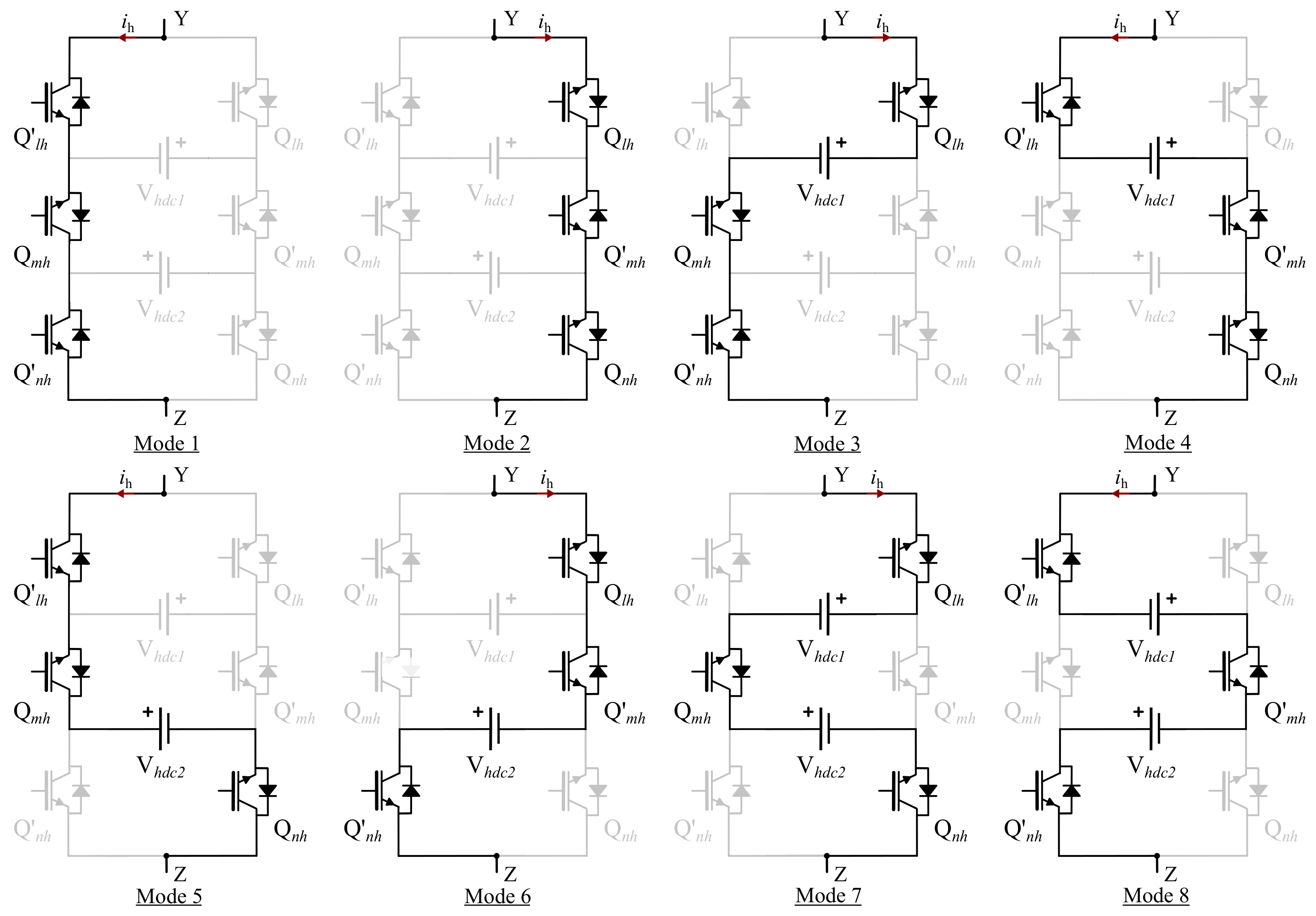
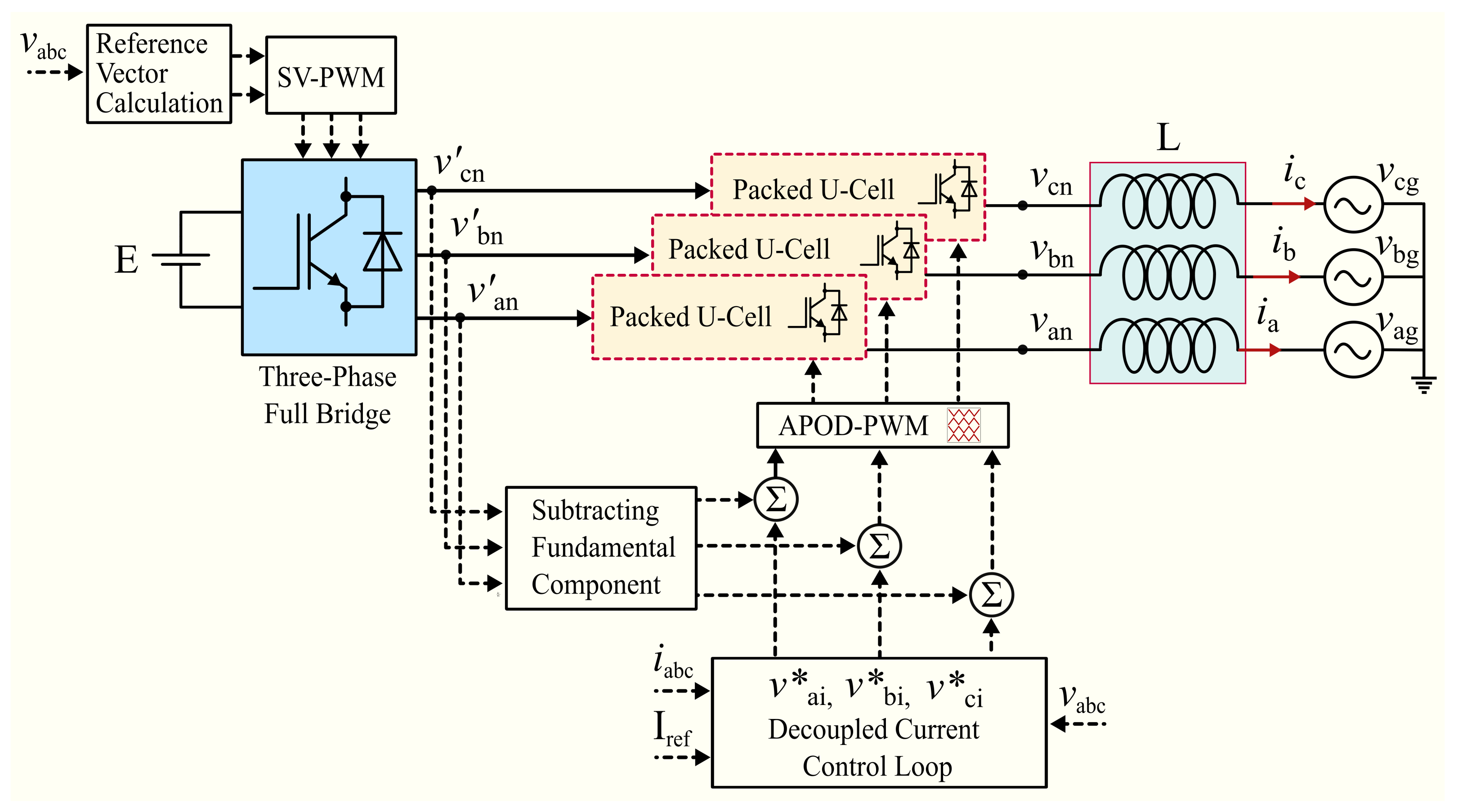
2. Proposed Converter Configuration

The proposed hybrid multilevel converter schematic shown in Figure 1 mainly consists of two parts: a three-phase full bridge and a packed U-cell. The three-phase full bridge consists of three half-legs, with each leg comprised of two alternately connected active switches, i.e., Q   1 and Q   4 (phase A). A main DC bus voltage E is connected in parallel to the three half-legs. As the switches operate alternately, they will produce voltages at the output (Y) having two levels, i.e., ±E. The packed U-cell connected in series consists of six active switches (Q   l h ,Q   m h , and Q   n h and Q   l h   , Q   m h   , and Q   n h   , respectively) and two DC link sources V   h d c 1 and V   h d c 2 (phases a, b, and c are subscripted as h). The DC links have an equal voltage of V   h d c 1 = V   h d c 2 = V   d c = 0.27E, which produces a five-level output voltage at the terminal ( v Y Z ), i.e., ±2V   d c , ±1V   d c , and 0. The five levels in the output voltage of the packed U-cell are ensured by the different switching modes. Also, the packed U-cell has redundancy in the switching state for ±1V   d c and 0 output voltage levels and has a unique state for ±2V   d c voltage level, as illustrated in Figure 2.
A switched equivalent model of the converter realizing the AC-side dynamics depicted in Figure 1 can be equated as Equation (1).
d i h d t = 1 L ( Q x h V h d c 1 + Q y h V h d c 2 Q z E ± v h g )
where v h g = V sin ( w t ) is the 50 Hz grid voltage, Q   z is the switching action and L is the inductor for A phase leg of a three-phase full bridge, whereas Q   x h and Q   y h are the packed U-cell switching actions (phases a, b, and c are subscripted as h), which are equated as Equations (2) and (3):
Q x h = Q l h Q m h Q l h Q m h
Q y h = Q m h Q n h Q m h Q n h

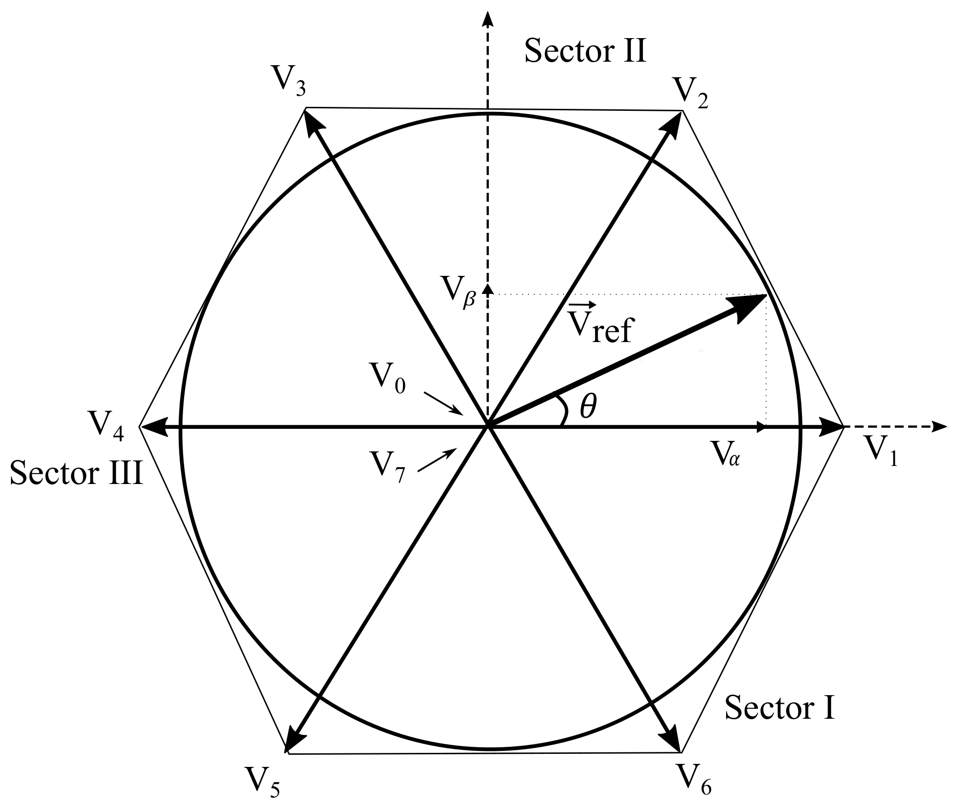
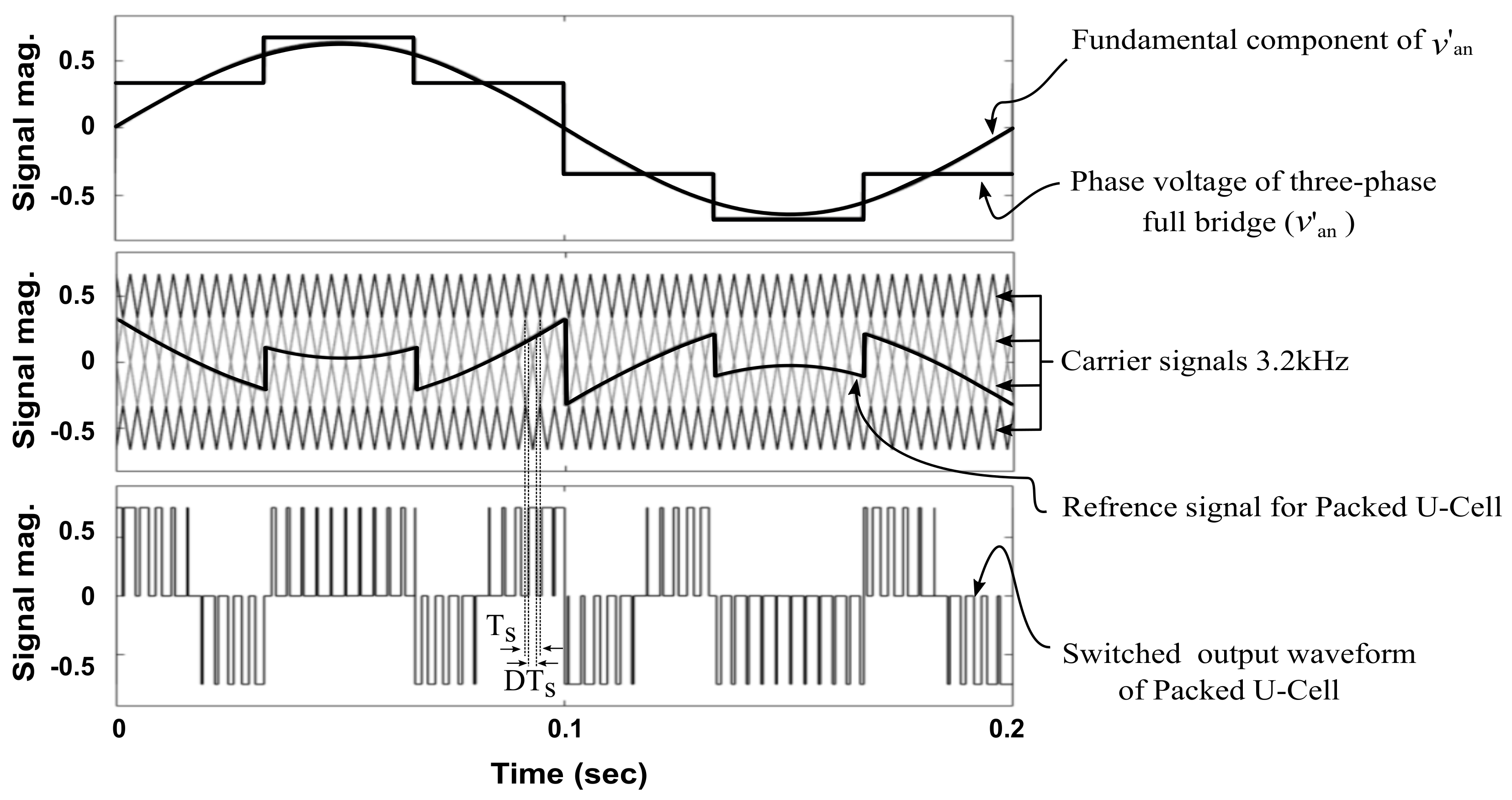
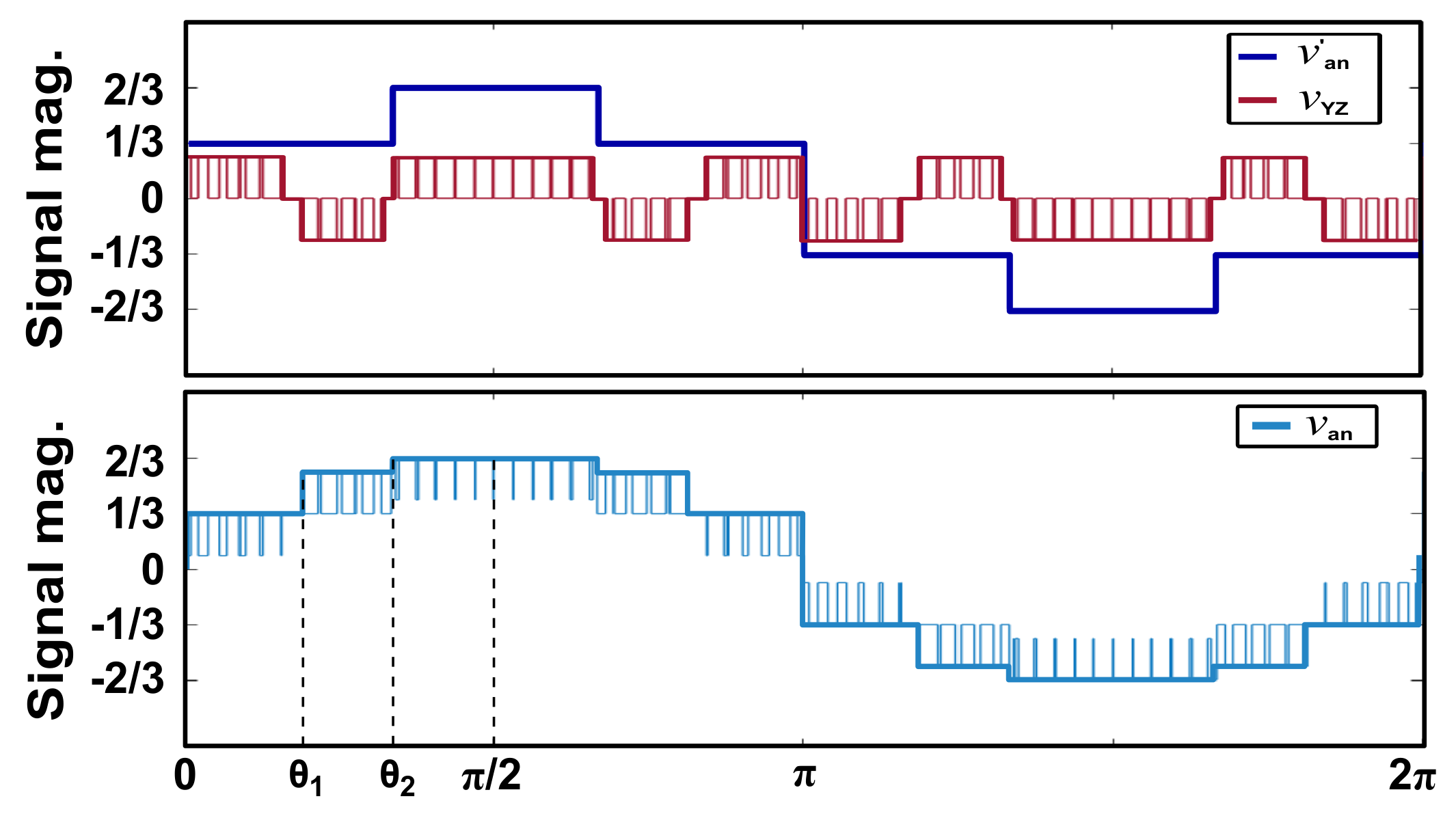
3. Hybrid Modulation Technique

The selection of a PWM strategy substantially influences switch loss within a given topology. PWM techniques involve approximating the converter output voltage levels based on a reference voltage. This study specifically aims to develop a modulation scheme that optimizes switch operation by considering their voltage stress, thus leading to reduced switching losses. Specifically, switches that handle high voltage stress should operate at a low switching frequency, while switches with lower voltage stress operate at a comparatively higher switching frequency. Therefore, the PWM technique is split into two parts: one for the three-phase full bridge and another for the series-connected packed U-cell. In the three-phase full bridge configuration, where switches endure high voltage stress, operate at low switching frequency, and limit the number of pulses per fundamental cycle. The switches in the packed U-cell are further classified based on their voltage stress, thus distinguishing between the high-voltage switches in the middle leg and the low-voltage switches in the outer leg. These categorizations will be elaborated on in a subsequent Section 3.2.

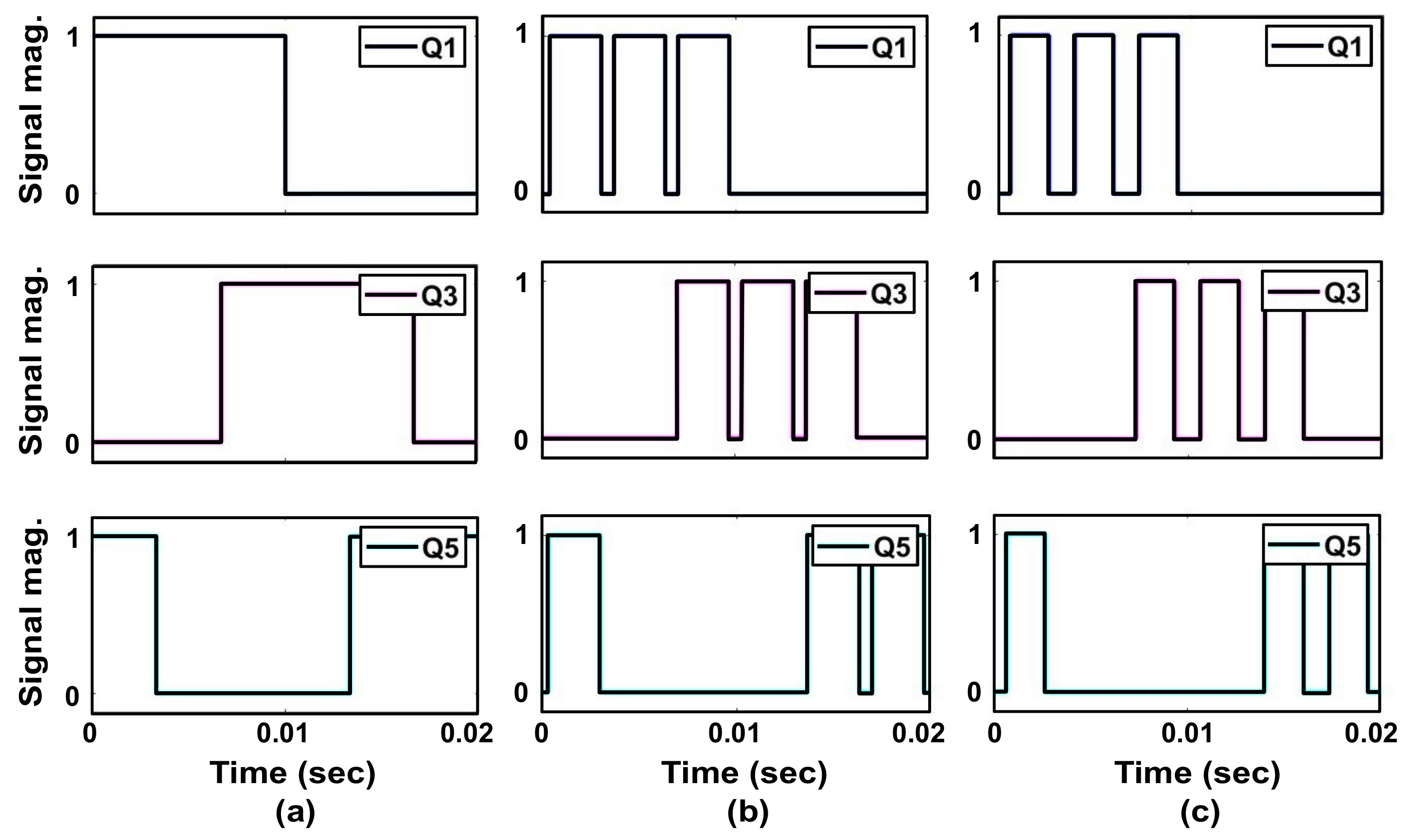
3.1. Modulation Strategy for Three-ph Full Bridge

Considering the three-phase full bridge shown in Figure 1, the switches bear high voltage stress. Therefore, SV-PWM, as a low-frequency switching modulation technique, is studied. For various switching combinations of a three-phase full bridge, the resulting output active state vectors correspond to vectors V   1 –V   6 in the α β coordinates, whereas vectors V   0 and V   7 , having zero magnitudes, are positioned at the center, as shown in Figure 3. To apply space vector modulation, the first step is to sample a reference signal, denoted as V r e f , at a frequency fs, where Ts represents the sampling period (Ts = 1/fs). The reference signal can be derived from three distinct phase references through the α β transform, as expressed by Equations (4)–(8).
V r e f = V α + V β = 2 3 ( V a + V b e j 2 π 3 + V c e j 2 π 3 )
V α = 2 3 ( V a + V b cos 2 π 3 + V c cos 2 π 3 )
V β = 2 3 ( V b sin 2 π 3 V c sin 2 π 3 )
V α V β = 2 3 1 1 2 1 2 0 3 2 3 2 V a V b V c
V r e f = V α 2 + V β 2
θ = tan 1 ( V β V α )
where θ is the angular displacement of the reference signal, which can be equated as Equation (9).
Different approaches are available for selecting the order of the vectors and determining which zero vector(s) to utilize. The choice of strategy impacts both the harmonic characteristics and the losses associated with switching. The SV-PWM modulation technique proposed in this study involves dividing the hexagon into three sectors. Within each sector, there are three active vectors. Considering sector I, the active state vectors V   6 , V   1 , and V   2 , and the zero state vectors V   0 and V   7 are applied for a duration of on-time period T   1 and off-time period T   0 , respectively. The on-time duration T   1 and the off-time duration T   0 can be expressed in terms of their angle and are given in Equations (10)–(12):
T 1 = 120 × M f
T 0 = 120 × ( 1 M f )
M f = 3 V r e f E
where M f represents the modulation index of a three-phase full bridge, whereas E represents the magnitude of the DC bus voltage. M f is a key factor in determining the time intervals T 1 and T 0 associated with applying active and zero vectors. Since the fundamental component of a three-phase full bridge remains in phase with the grid voltage, any changes in the M f will lead to variations in the on-time and off-time durations. Figure 4 depicts pole voltages of the switches (Q   1 , Q   3 , and Q   5 ) of the three-phase full bridge at different modulation indexes.

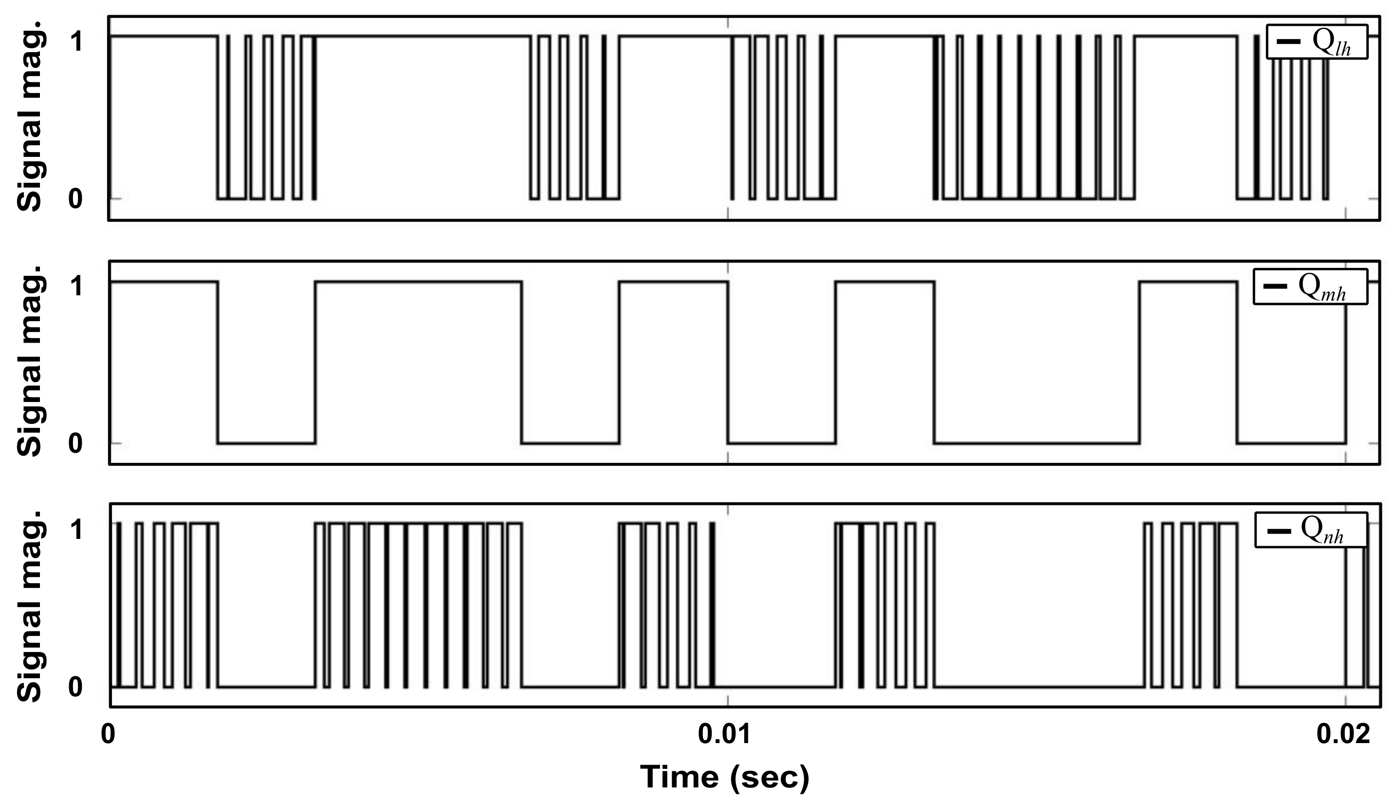
3.2. Modulation Strategy for Packed U-Cell

Considering the converter’s design aspect, the packed U-cell consists of three pairs of active switches that complement each other. These active switches are divided into categories based on the voltage stresses they handle, i.e., high-frequency active switches and low-frequency active switches. The middle complement pair switches in the packed U-cell, namely (Q   m h and Q m h ), which experience a high voltage stress of 2 V   d c . These switches are operated at a switching frequency of 250 Hz, which helps to minimize switching loss. On the other hand, the outer complement pair switches, namely (Q   l h , Q   n h , and Q l h , as well as Q n h ), in the packed U-cell bear a low voltage stress of V   d c . As a result, these switches operate at a switching frequency seven times higher than the middle complement pair switches, as depicted in the Figure 5.
For the packed U-cell, an APOD-PWM modulation technique is adopted, as shown in Figure 6, which has an equivalent carrier frequency of 3.2 kHz. This modulation technique is employed to generate voltage levels. However, the effective frequency of the APOD-PWM is 1.6 kHz. This low effective frequency is beneficial, as it helps distribute switch losses more evenly throughout the system.
The magnitude of the reference signal has an impact on the output voltage of the packed U-cell. Since the packed U-cell functions as a cascade filter, the reference signal for this module is derived by subtracting its fundamental component from the phase output voltage. In this particular case, a modulation index M f = 1 is assumed for the three-phase full bridge converter. As a result, the packed U-cell’s reference signal produces three output voltage levels, which are depicted as the switched output waveform of the packed U-cell in Figure 6.
The mathematical expression of the output a-phase leg voltage can be expressed by Equation (13) through Equation (16).
v a n = v a n v Y Z
v a n = 4 3 π E r 1 r ( cos ( π 3 r + θ f ) + M f ) ( sin ( r ω t ) )
v a n f u n d a m e n t a l = 4 3 π E ( cos ( π 3 + θ f ) + M f ) ( sin ( ω t ) )
v Y Z = v a n v a n f u n d a m e n t a l
The θ f value is determined by the T   0 duration of SV-PWM calculated in the three-phase full bridge converter. This off-time interval T   0 is subject to change based on the modulation depth M f of the three-phase full bridge converter, while r represents harmonic component order.
The output voltage levels of the packed U-cell, with lower DC link voltage requirements for harmonic minimization, will be accommodated within the fundamental converter output voltage. This results in an overall multilevel phase voltage (a-phase leg), with a nonuniform voltage step presented in Table 1, and is illustrated by Figure 7.

3.3. Modulation Range

The maximum output voltage of the packed U-cell, when employing the SV-PWM modulation strategy, is dependent on the modulation index M f of the three-phase full bridge. The choice of modulation index range significantly impacts the required DC link’s voltage for effective harmonic minimization.
When the maximum modulation index M f is set to 1, the sum of the DC link’s voltage, i.e., V   h d c 1 + V   h d c 2 , must be ( 1 3 )E, where E is the DC bus voltage. However, if the modulation index of the fundamental converter is slightly reduced to M f = 0.95, the total DC link’s voltage required for minimizing the harmonics generated by the fundamental converter becomes ( 1 2 )E. Figure 8 depicts the sum of the DC link’s voltage requirement at different modulation indexes.
Decreasing the total DC link’s voltage requirements for harmonic compensation minimizes the voltage stress on the semiconductor switches. This approach offers an advantage compared to adjusting the switching frequency based on the system design, as it helps to reduce the overall voltage stress on the components.

3.4. Switch Losses

The switch losses of any topology can be categorized into conduction losses and switching power losses. Grouping the total power switch losses P T by different power converter topologies is a reasonable approach, as it allows for a more detailed and meaningful comparison of the losses across various converter configurations. The proposed topology studied in this paper consists of 24 power switches with antiparallel diodes. The switch loss model has been implemented in the MATLAB–Simulink environment given in [45,46].
The conduction losses P c d in a power converter are determined by the power dissipated through the power switches p s w and their corresponding diodes d. The direction of the current flow plays a crucial role in the calculation of these conduction losses. The P c d , at any given instant across an active power switch ( p s w ) and its corresponding diode (d), can be calculated using the given Equation (17) through Equation (19).
P c _ ( n p s w ) = 1 2 π 0 2 π ( n p s w × v p s w ) i c o n d · Z l d ( ω t )
P c _ ( n d ) = 1 2 π 0 2 π ( n d × v d ) i c o n d · Z l d ( ω t )
P c d = P c _ ( n p s w ) + P c _ ( n d )
where n p s w and n d are the semiconductor device count, and v p s w and v d are their associated voltage drops during the conduction state, respectively. whereas, i c o n d is the conduction current, and Z l is the switching action of the active switch.
The switching losses of the active switch can be evaluated for each turn-on and turn-off transition that occurs during a reference period. The total switching losses over this reference period can then be determined using the following Equations (20) and ():
P s w = P s w _ O N + P s w _ O F F
= j = 1 2 n + 2 1 6 v x ( j ) · i c o n d · ( t O N + t O F F ) f s w ( j )
where v x ( j ) and f s w ( j ) are the blocking voltage and the switching frequency of the active semiconductor devices, respectively.
The total power switch losses, denoted as P T , across the power converter can be computed as the sum of the conduction losses P c d and the switching losses P s w , as shown in the following Equation (22):
P T = P c d + P s w

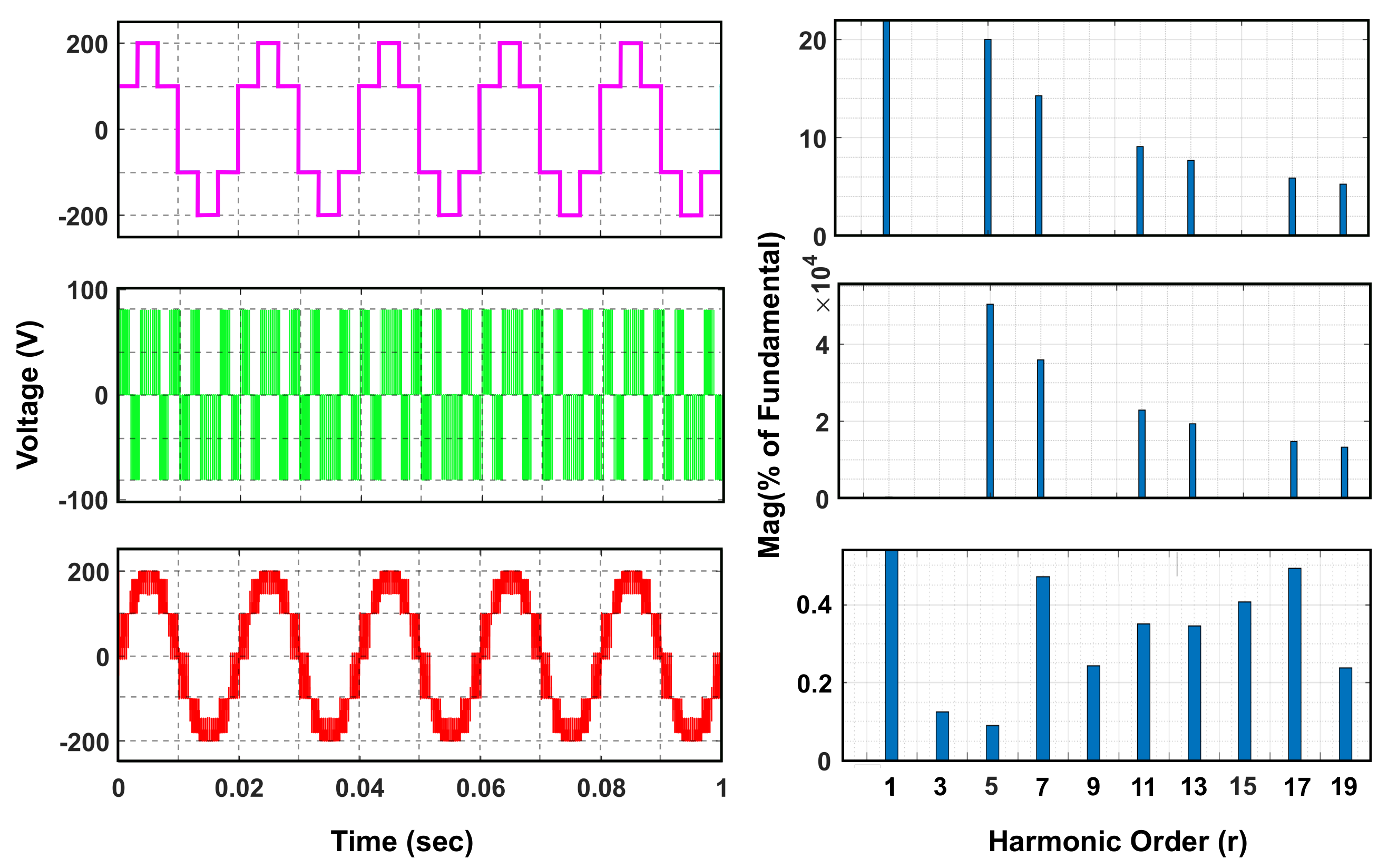
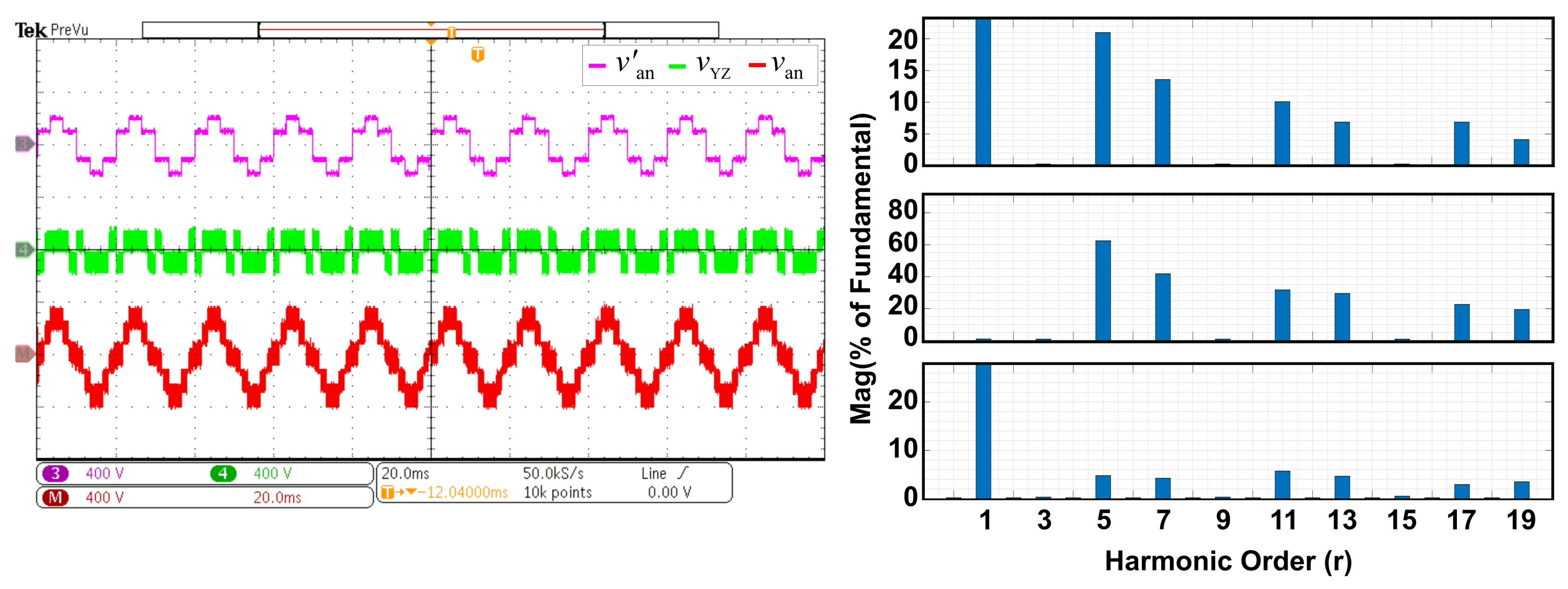
3.5. Total Harmonic Distortion
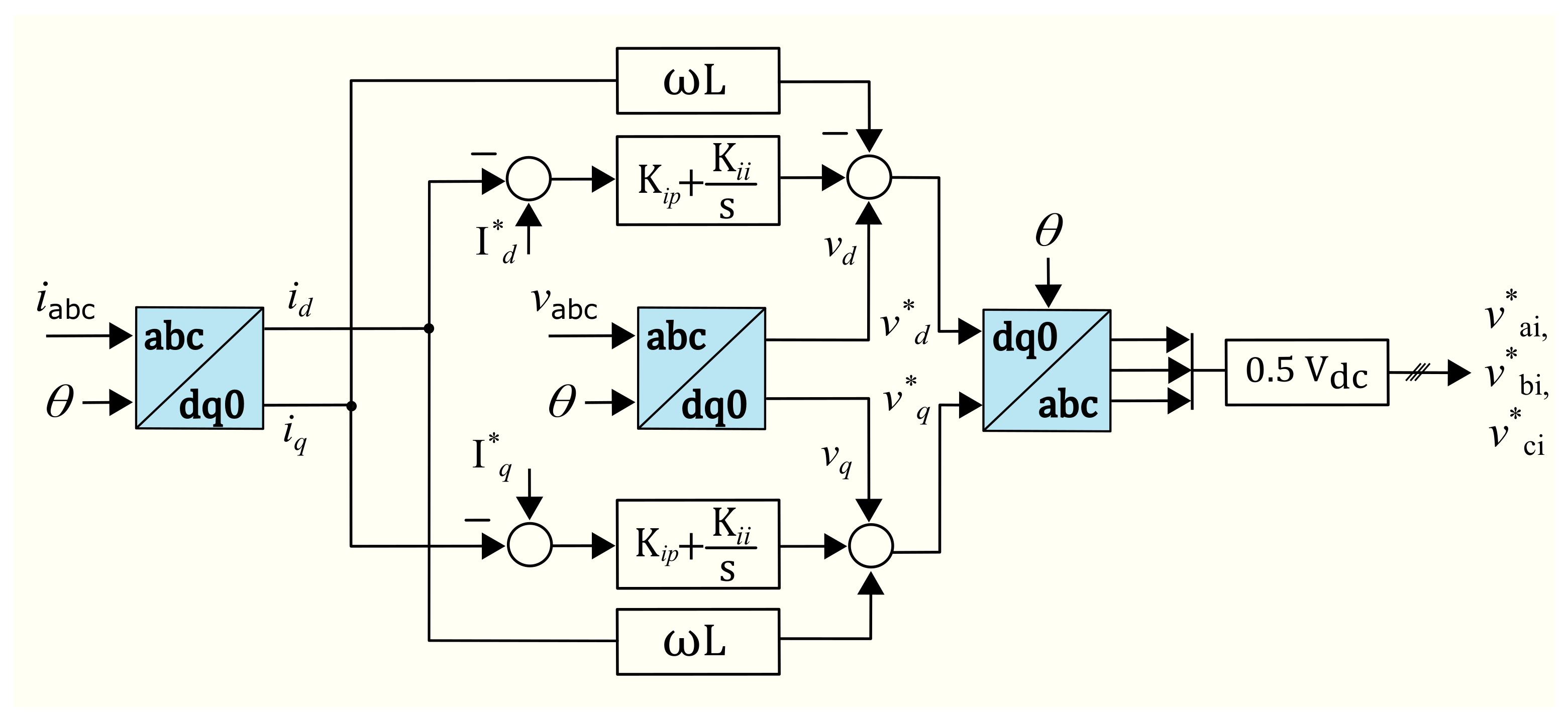
The total harmonic distortion (THD) is defined as the ratio of the equivalent root mean square (RMS) voltage of all the harmonic frequencies (from the 2nd harmonic on) over the RMS voltage of the main frequency of the signal (fundamental frequency) that is calculated using Equation (23).
T H D = m = 2 V m 2 V f
where V m and V f are the RMS voltage values of the mth harmonic and fundamental frequency, respectively. It is important to note that while this equation uses voltage as the parameter, the same mathematical definition can be applied to the current THD as well by replacing the voltage terms with their corresponding current values. The calculation of the voltage THD involves performing a Fourier analysis on the voltage waveform, which determines the magnitudes of the fundamental and harmonic components. The amplitudes of these individual frequency components are determined using the Fourier analysis, as given in Equation (13) through Equation (16). This information is then used to compute the voltage THD using the Equation (23).

4. Control Scheme

This control strategy’s main objective is to ensure that the necessary voltage is provided to achieve the desired output current. This control approach operates through two main pathways: the three-phase full bridge, which offers the fundamental component support in the feedforward path, and the packed U-cell, which supports controlling harmonics and achieving fast current response. These pathways are shown in Figure 9. The current control is specifically implemented in the packed U-cell, as these cells deliver high-frequency support. As a result, the system can swiftly react to sudden changes in the grid voltages.

Feedback Control Mechanism

The performance of a converter system is heavily dependent on the effectiveness of its current control. Robust current control is essential to ensure a fast transient response and satisfactory steady state behavior. One widely adopted approach is current control in the synchronous reference frame (SRF), also known as the dq coordinate system [47].
The SRF-based current control offers several attractive features that have made it a popular choice in most pulse-width modulation (PWM) schemes. The dq coordinate transformation allows for the decoupling of the AC current components, thus enabling independent control of the active and reactive power components. This simplifies the design of the current regulators and facilitates the implementation of advanced control algorithms.
Furthermore, the SRF-based current control enables the use of proportional–integral (PI) regulators, which are relatively easy to tune and provide good steady state performance. The transformation to the dq frame also helps mitigate the effects of grid frequency variations, as the control variables become DC quantities in the steady state. Referring to Figure 1, the following current–voltage equation Equation (24) is deduced by ignoring the resistive components.
V a g V b g V c g V a n V b n V c n = L d d t i a i b i c
The Park transformation matrix, given in the reference [48] and expressed as Equation (25) to Equation (27), facilitates the conversion of the three-phase voltage and current into their corresponding d–q components.
T P = 2 3 sin ( ω t ) sin ( ω t 2 3 π ) sin ( ω t + 2 3 π ) cos ( ω t ) cos ( ω t 2 3 π ) cos ( ω t + 2 3 π )
Therefore
v d v q = T P V a n V b n V c n
i d i q = T P i a i b i c
Given a balanced three-phase condition, when the voltage vector V g aligns with the d axis, the corresponding v q component will be zero. Applying the d–q transformation, the active power and reactive power can be expressed as follows:
P = 3 2 ( v d i d ) + ( v q i q )
Q = 3 2 ( v q i d ) ( v d i q )
The active power P and reactive power Q can be effectively regulated by independently controlling the i d and i q components of the current vector. The current commands I d * and I q * in the respective axes are expressed by equations (Equation (30)) and (Equation (31)):
I d * = p * v d
I q * = q * v q = 0
The active and reactive power components are denoted as p * and q * , respectively. To ensure system operation at a unity power factor, setting q * = 0 is necessary.
As shown in Figure 10, the active and reactive current references, I d * and I q * , can be directly derived from the grid’s active and reactive power p * and q * , respectively. The control loop utilizes the d- and q-axis grid voltage components, v d and v q , as well as the filter inductor L.
Based on these input variables, the d- and q-axis voltage references for the system, v d * and v q * , can be calculated using Equation (32):
v d * v q * = v d 0 + 0 ω L ω L 0 i d i q + K i p I d * i d I q * i q + K i i I d * i d I q * i q d t
where K i p and K i i are the proportional and integral gain of the current control. The d and q axes are rotating with an angular velocity equal to ω . Control signals v a i * , v b i * , and v c i * , which are attained after inverse d–q to abc transformation, are then utilized to drive the packed U-cell shown in Figure 9.

5. Results and Discussion

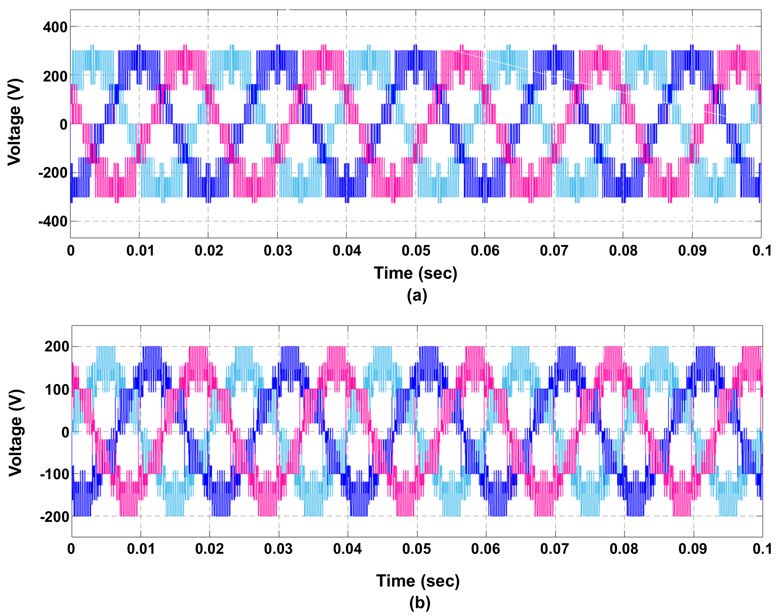
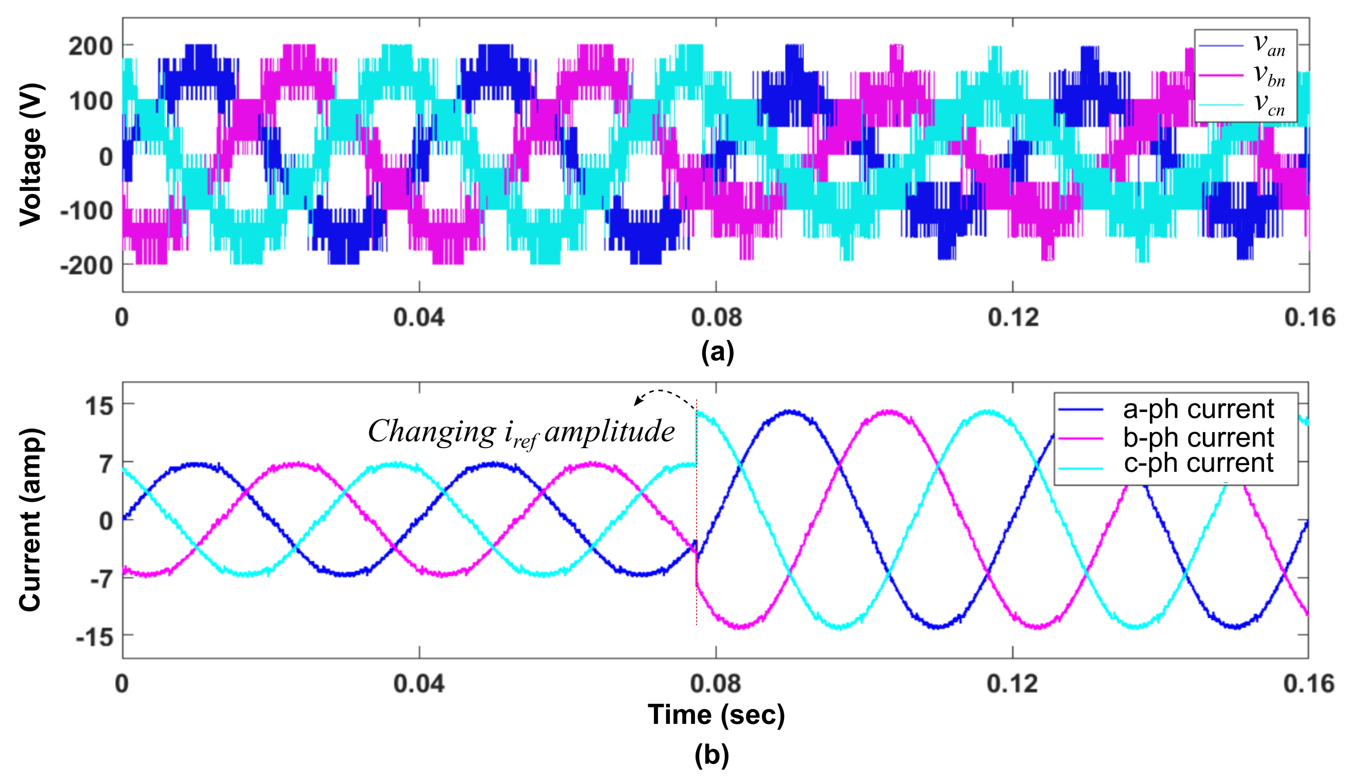
5.1. Simulation Results

The study conducted a simulation of the proposed hybrid MLC configuration given in Figure 1, using the MATLAB/Simulink platform. The parameters of the proposed topology configuration are listed in Table 2. The simulation settings were carefully adjusted to ensure consistency between the simulation findings and the experimental results.
The outer-leg complement pair of switches in the packed U-cell (Q   l h , Q   n h , and Q   l h , as well as Q   n h ) are operated at a switching frequency of 3.2 kHz, thus resulting in an effective switching frequency of 1.6 kHz. This selection of the switching frequency offers several benefits to the hybrid MLC configuration, including reduced current ripple, smaller inductor size, and lower overall system costs, thereby enhancing the system’s performance and cost-effectiveness. The considered value for the DC-bus voltage was set to E = 300 V, while the DC link voltage required for harmonic compensation by the packed U-cell was kept slightly higher, i.e., V d c = 85 V. This slight increase in the DC link voltage ensures coverage of the entire range of the modulation index to mitigate the harmonics produced by the three-phase full bridge, as shown in Figure 8.
The Figure 11 depicts the output voltage waveform and its corresponding harmonic spectrum at the maximum modulation index of a single leg (Leg-A) of the proposed converter, as depicted in Figure 1. The terminal voltage v a n of the three-phase full bridge generates a staircase waveform by employing a low switching frequency, which helps to minimize switching losses. However, this results in harmonics that violate the permissible range according to IEEE standard 519. To address the power quality issue, a packed U-cell was used as a cascade filter with a switching frequency of 3.2 kHz. This packed U-cell generates an output voltage v Y Z that contains only the harmonics, thus effectively filtering out the unwanted harmonics when added to the three-phase full bridge. As a result, the overall output voltage v a n becomes a seven-level output with harmonics that fall within the permissible range specified by the IEEE standard, i.e., an individual harmonic < 5 % .
Figure 12 shows the three-phase multilevel terminal voltage of the proposed converter at a maximum M f . In Figure Figure 12a, the line voltage is depicted as v L L = 3 v a n , while Figure 12b illustrates the seven-level phase voltage v a n of the converter.
Figure 13 shows the three-phase multilevel terminal voltage of the proposed topology at M f = 0.9. In Figure 13a, the line voltage is given, while Figure 13b shows the phase voltage v a n of the converter.
The proposed converter’s output voltage and current waveforms are shown in Figure 14. Figure 14a shows the phase voltages, whereas Figure 14b illustrates the converter’s current. It is evident from the waveform that the current control in the dq reference coordinates tracked its reference value as the amplitude varied from 50% to a 100% power rating.

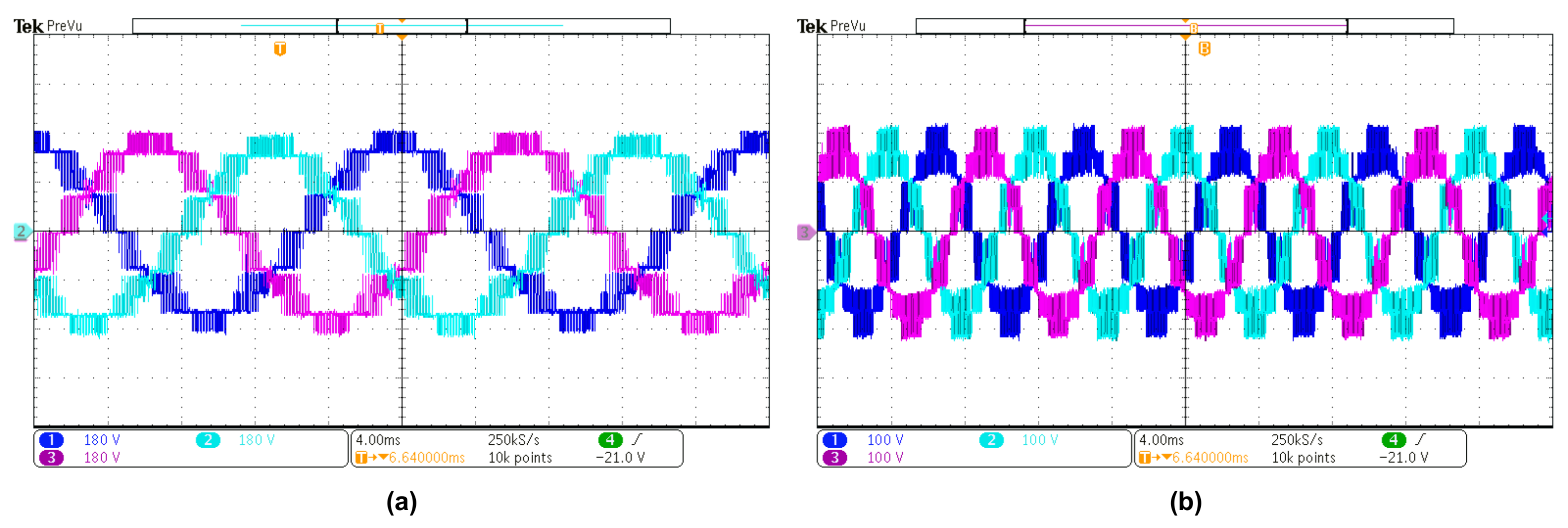
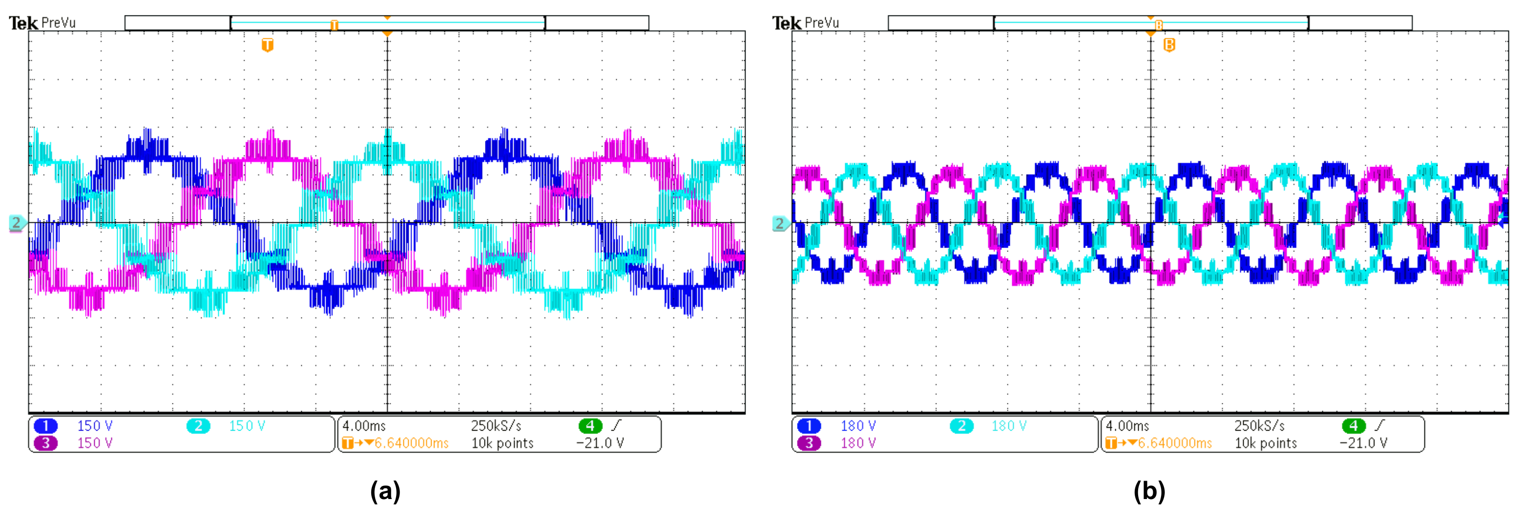
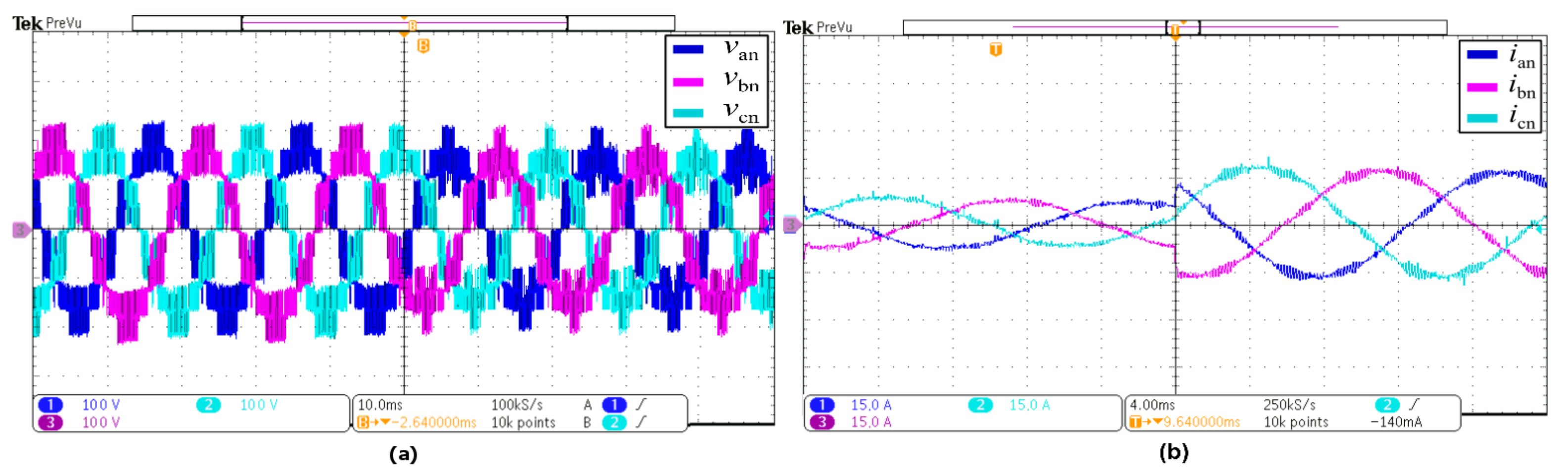
5.2. Experiment Results

As shown in Figure 15, a low-voltage laboratory setup was used to experimentally validate the proposed hybrid MLC topology and its modulation and control strategy. A custom control board was designed and fabricated to realize the control scheme in practice, thus incorporating a control unit (TMS320C28346 DelfinoTM, by Texas Instruments (Dallas, TX, USA)), a programmable logic device (EPM570 ALTERA®, field-programmable gate array (FPGA) by Altera Corporation (San Jose, CA, USA)), and analog to digital conversion AD7656 by Analog Devices (Norwood, MA, USA). Moreover, a laboratory setup of the proposed converter was constructed, thus consisting of two power boards, with each equipped with six insulated-gate bipolar transistors (IGBTs), as well as voltage and current sensors. The converter was connected to a 110V RMS grid to emulate realistic operating conditions. As detailed in the following section, the experimental findings exhibit a strong agreement with the simulation waveforms.
Figure 16 depicts the experimental waveforms of the proposed hybrid MLC (Multilevel Converter). Each waveform is accompanied by its corresponding Fast Fourier Transform (FFT) analysis, which were generated in MATLAB from real-time experimental data. The output voltage of the three-phase full bridge v a n exhibited significant harmonic components due to the low switching of high-voltage stressed switches in a module to minimize switching losses. However, the harmonics produced by the three-phase converter v Y Z were significantly high, which were effectively filtered out by the packed U-cell connected in series. As a result, the overall output voltage v a n of the hybrid MLC adheres to the harmonics range specified by IEEE standards.
Figure 17 illustrates the experimental results of the proposed three-phase hybrid multilevel converter output voltage at a maximum M f of 1. In Figure 17a, the line voltage waveform is depicted as v L L = 3 v a n , while Figure 17b illustrates a seven-level phase voltage waveform v a n of the converter. Similarly, Figure 18 shows the experimental results of the proposed three-phase hybrid multilevel converter output voltage at an M f of 0.9. In Figure 18a, the line voltage is depicted, while Figure 18b illustrates the phase voltage v a n of the converter.
The proposed converter’s experimental terminal voltage waveforms and current waveforms are shown in Figure 19. Figure 19a shows the experimental phase voltage waveform, whereas Figure 19b illustrates the experimental converter’s current waveform. Notably, the experimental waveforms demonstrate that the current control in the dq reference coordinates effectively tracked its reference value as the power amplitude varied from 50% to 100% of the rating. Furthermore, the experimental waveforms closely align with the simulation results, thus indicating a clear match between the two.

6. Comparative Analysis

Selecting an appropriate topology and the semiconductor components for a specific application is crucial from a technical aspect. Various procedures and comparisons have been carried out [49,50]. For instance, the industrial drives market offers a range of equipment solutions that employ different topologies and semiconductor technologies. Some designs utilize the traditional 3L NPC VSC with IGCTs, while others adopt this approach using IGBTs [49]. This section highlights the proposed converter scheme’s performance and efficiency by comparing it with other medium-voltage converters, i.e., the five-level FC-based ANPC and the MMC, which are commercially well known, while other possible and noncommercial configurations are also discussed.

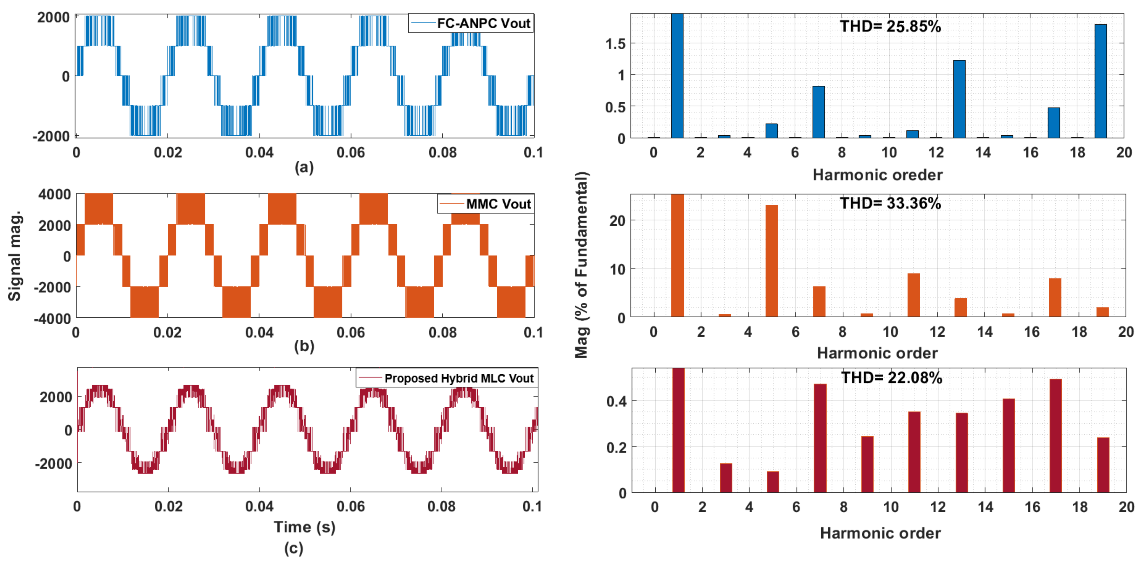
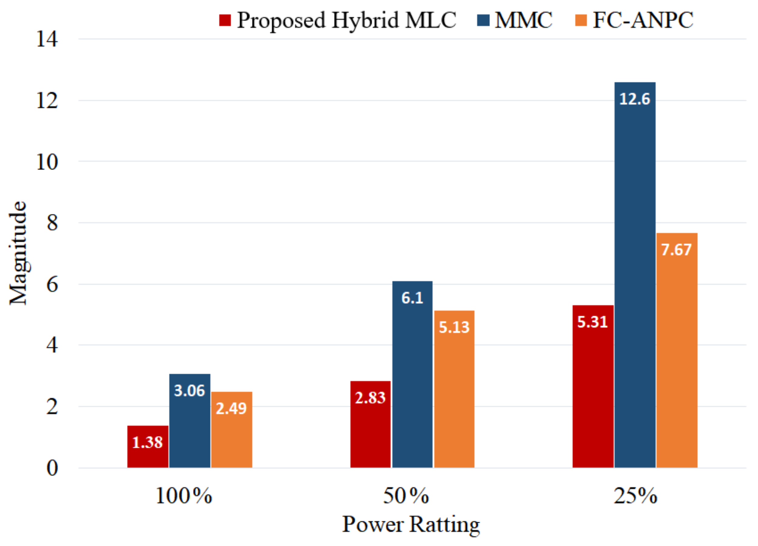
6.1. Comparison Based on Voltage and Current THD

A five-level FC-based ANPC converter [28] utilizing carrier-based PWM has been simulated in MATLAB/Simulink, with the parameters listed in Table 3. It was assumed that the DC link capacitors C1 and C2 and the flying capacitors (C3) were initially charged to 2 kV and 1 kV, respectively. The topology was connected to a common DC bus of 4 kV. For grid-connected applications, a carrier frequency of approximately 3 kHz was used for the carrier-based PWM [51]. The measured phase voltage waveform and its associated harmonic spectrum are shown in Figure 20a. In terms of percentage, the THD of the phase voltage came out to 25.85%. The current control loop, which was composed of the feedforward and the proportional feedback control loop, was deployed. The current THD percentages of 7.67%, 5.13%, and 2.49% were achieved while operating the converter at 25%, 50%, and 100% power ratings, respectively.
The second selected five-level MMC converter discussed in [35] was also analyzed in this study with identical power and voltage conditions under phase shift PWM. The carrier frequency of the phase shift PWM was considered to be 1.6 kHz. The measured phase voltage waveform and its harmonic spectrum are shown in Figure 20b. In terms of percentage, the THD of the phase voltage came out to 33.36% due to the bigger step size. The current THD percentages of 12.6%, 6.11%, and 3.06% were achieved while operating the converter at 25%, 50%, and 100% power ratings, respectively.
To evaluate the performance of the proposed converter with similar power conditions, the proposed hybrid MLC topology under the hybrid modulation and control method was simulated in the MATLAB/Simulink environment. The hybrid control strategy implements the APOD-PWM control method with a 3.2 kHz carrier frequency. The measured phase voltage waveform and its harmonic distortion spectrum are shown in Figure 20c. Due to the smaller step size, as discussed in Section 3 and Section 3.2, the percentage THD of the phase voltage came out to 22.08%. The current THD percentages of 5.31%, 2.83% and 1.38% were achieved while operating the converter at 25%, 50%, and 100% power ratings, respectively. The current THD values for the converters mentioned, operating at various power ratings, are provided in Figure 21. This figure illustrates that the proposed hybrid MLC converter exhibited a lower current THD compared to the FC-based ANPC and MMC converter topologies discussed in this study.

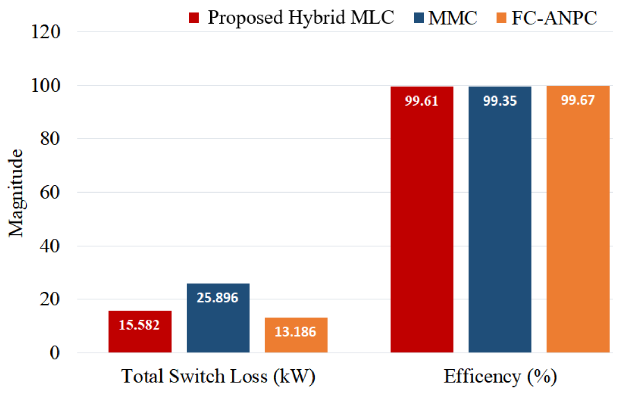
6.2. Comparison Based on Converter Switch Loss and Efficiency

To quantify the feasibility of the proposed hybrid MLC topology, this section will compare the power semiconductor loss and efficiency with the FC-based ANPC and the MMC configurations. The selected topologies were compared using power semiconductor devices available at various voltage levels, as detailed in Table 4. In this study for switch loss calculation, IGCTs were used in the case that the device voltage stress was greater than 2.5 kV due to their lower conduction losses, wherein the maximum power output was fixed at 4 MW. The detailed switch loss model has been implemented in the MATLAB–Simulink environment given in [45,46], with the converter systems parameters listed in Table 3. The power losses associated with semiconductor devices, such as IGCTs, IGBTs, and antiparallel diodes, have been categorized into conduction losses and switching losses.
The efficiency of any converter topology is determined by the power loss due to semiconductor switches utilized to attain the desired characteristics. The MMC configuration was simulated under phase shift PWM with a 3.2 kHz carrier frequency, thus resulting in an equivalent switching frequency of 1.6 kHz per arm with reduced switch loss. Figure 22 depicts the proposed hybrid MLC’s measured switch loss and efficiency, which is compared with the FC-based ANPC and the MMC topologies. It has been observed that the efficiency of the proposed hybrid MLC configuration was marginally reduced (0.06%) compared to the FC-ANPC and 0.26% higher than the MMC configuration. This indicates the effectiveness of the proposed hybrid MLC topology and confirms it as a viable option for medium-voltage applications.

6.3. Comparison Based on Component Count

The overall cost of a converter configuration is determined by the number of components used in its topology. By carefully analyzing the component count associated with different converter topologies, one can make an informed decision about which topology is the most economical for any specific application. Therefore, it is important to consider the converter configuration that achieves more levels in the output voltage while using the fewest components. Table 5 provides information regarding the component counts for each discussed converter configuration in Section 1, along with the corresponding total output voltage levels. In [30,35,52], a higher number of components was used, thus resulting in a five-level voltage. On the other hand, the topology described in [29] employed fewer components but created a three-level voltage; similarly, in [28], they utilized the same number of components but generated a five-level voltage. In contrast, the proposed converter configuration, similar to the topology configuration in [33], utilized the minimum number of components while achieving a seven-level voltage at the terminal.

7. Conclusions

This article introduced an innovative hybrid three-phase multilevel topology and a hybrid modulation and control strategy specifically designed for lower- to medium-voltage front-end converters. The proposed topology configuration combines a packed U-cell in series with a three-phase full bridge that generates seven levels of output voltage. The desired voltage levels were achieved by utilizing eight semiconductor devices and two DC link sources per leg connected to a common main DC bus voltage. The control of the active switches was optimized by implementing suitable switching frequencies using low-frequency SV-PWM and high-frequency APOD-PWM techniques. Furthermore, a comprehensive comparison with relevant topologies demonstrated that the proposed hybrid topology offered several advantages. These include (i) reduced voltage and current total harmonic distortion (THD), (ii) minimized switch loss, (iii) improved overall efficiency, and (iv) a decreased component count, while achieving increased output voltage levels. The simulation and experimental results from a laboratory prototype were provided, thus confirming the effectiveness of the proposed hybrid MLC configuration and its hybrid modulation and control strategy. The proposed solution is a promising approach to utilize existing energy resources in medium-voltage converter applications efficiently.

Author Contributions

Conceptualization, M.A. and M.M.K.; methodology, M.T.F.; software, M.A. and M.M.K.; validation, M.A. and M.M.K.; formal analysis, M.A. and M.T.F.; investigation, M.T.F.; resources, M.M.K.; data curation, M.A.; writing—original draft preparation, M.A.; writing—review and editing, M.A. and V.N.; visualization, M.T.F. and V.N.; supervision, M.M.K., V.N. and K.-H.L.; writing—review and editing, project administration, funding acquisition, M.M.K., V.N. and K.-H.L. All authors have read and agreed to the published version of the manuscript.

Funding

This research received no external funding.

Data Availability Statement

The original contributions presented in the study are included in the article, further inquiries can be directed to the corresponding author.

Acknowledgments

The work presented in this article is supported by the Centre for Advances in Reliability and Safety (CAiRS), admitted under the AIR@InnoHK Research Cluster.

Conflicts of Interest

The authors declare no conflict of interest.

References

  1. Alahmad, A.; Kaçar, F. Medium-Voltage (MV) Motor Drives Topologies and Applications. In Proceedings of the 2022 International Conference on Electrical, Computer and Energy Technologies (ICECET), Prague, Czech Republic, 20–22 July 2022; pp. 1–5. [Google Scholar] [CrossRef]
  2. Sharifi, S.; Ferencz, I.F.; Kamel, T.; Petreuş, D.; Tricoli, P. Medium-voltage DC electric railway systems: A review on feeding arrangements and power converter topologies. IET Electr. Syst. Transp. 2022, 12, 223–237. [Google Scholar] [CrossRef]
  3. Rahouma, A.; Oggier, G.G.; Balda, J.C. A Review of Medium-Voltage Front-End Converters for Grid-Connected Battery Energy Storage Systems. In Proceedings of the 2022 IEEE 13th International Symposium on Power Electronics for Distributed Generation Systems (PEDG), Kiel, Germany, 26–29 June 2022; pp. 1–7. [Google Scholar] [CrossRef]
  4. Rabiul Islam, M.; Mahfuz-Ur-Rahman, A.M.; Muttaqi, K.M.; Sutanto, D. State-of-the-Art of the Medium-Voltage Power Converter Technologies for Grid Integration of Solar Photovoltaic Power Plants. IEEE Trans. Energy Convers. 2019, 34, 372–384. [Google Scholar] [CrossRef]
  5. IEEE Std 519-2022 (Revision of IEEE Std 519-2014); IEEE Standard for Harmonic Control in Electric Power Systems. IEEE: Piscataway, NJ, USA, 2022; pp. 1–31. [CrossRef]
  6. Mondol, M.H.; Biswas, S.P.; Rahman, M.A.; Islam, M.R.; Mahfuz-Ur-Rahman, A.M.; Muttaqi, K.M. A New Hybrid Multilevel Inverter Topology With Level Shifted Multicarrier PWM Technique for Harvesting Renewable Energy. IEEE Trans. Ind. Appl. 2022, 58, 2574–2585. [Google Scholar] [CrossRef]
  7. Fazel, S.S. Investigation and Comparison of Multi-Level Converters for Medium Voltage Applications. 2007. Available online: https://depositonce.tu-berlin.de/items/6cd2e1d6-ae7f-42b5-8bb7-0410560b21b4 (accessed on 11 June 2021).
  8. Krug, D.; Bernet, S.; Fazel, S.S.; Jalili, K.; Malinowski, M. Comparison of 2.3-kV Medium-Voltage Multilevel Converters for Industrial Medium-Voltage Drives. IEEE Trans. Ind. Electron. 2007, 54, 2979–2992. [Google Scholar] [CrossRef]
  9. Tolbert, L.; Peng, F.Z.; Habetler, T. Multilevel converters for large electric drives. IEEE Trans. Ind. Appl. 1999, 35, 36–44. [Google Scholar] [CrossRef]
  10. Nabae, A.; Takahashi, I.; Akagi, H. A New Neutral-Point-Clamped PWM Inverter. IEEE Trans. Ind. Appl. 1981, IA-17, 518–523. [Google Scholar] [CrossRef]
  11. Alepuz, S.; Busquets-Monge, S.; Bordonau, J.; Gago, J.; Gonzalez, D.; Balcells, J. Interfacing Renewable Energy Sources to the Utility Grid Using a Three-Level Inverter. IEEE Trans. Ind. Electron. 2006, 53, 1504–1511. [Google Scholar] [CrossRef]
  12. Franquelo, L.G.; Rodriguez, J.; Leon, J.I.; Kouro, S.; Portillo, R.; Prats, M.A. The age of multilevel converters arrives. IEEE Ind. Electron. Mag. 2008, 2, 28–39. [Google Scholar] [CrossRef]
  13. Lai, J.S.; Peng, F.Z. Multilevel converters-a new breed of power converters. IEEE Trans. Ind. Appl. 1996, 32, 509–517. [Google Scholar] [CrossRef]
  14. Goel, R.; Dey, A. Higher Level Multilevel Inverter for Medium Voltage Drives with High DC-link Voltage Utilization. In Proceedings of the 2020 IEEE International Conference on Power Electronics, Drives and Energy Systems (PEDES), Jaipur, India, 16–19 December 2020; pp. 1–6. [Google Scholar] [CrossRef]
  15. Hammond, P. A new approach to enhance power quality for medium voltage drives. In Proceedings of the Industry Applications Society 42nd Annual Petroleum and Chemical Industry Conference, Denver, CO, USA, 11–13 September 1995; pp. 231–235. [Google Scholar] [CrossRef]
  16. Zolfagharian, O.; Farsijani, M.; Keyvanloo, E.; Tavakoli Bina, M. A New Modulation Technique for Improving the Performance of Two-Phase Cascaded H-bridge Multilevel Inverter. In Proceedings of the 2022 13th Power Electronics, Drive Systems, and Technologies Conference (PEDSTC), Tehran, Iran, 1–3 February 2022; pp. 202–206. [Google Scholar] [CrossRef]
  17. Ipoum-Ngome, P.G.; Mon-Nzongo, D.L.; Flesch, R.C.C.; Tang, J.; Jin, T.; Wang, M.; Lai, C. Multiobjective Model-Free Predictive Control for Motor Drives and Grid-Connected Applications: Operating with Unbalanced Multilevel Cascaded H-Bridge Inverters. IEEE Trans. Power Electron. 2023, 38, 3014–3028. [Google Scholar] [CrossRef]
  18. Guo, X.; Wang, X.; Wang, C.; Lu, Z.; Hua, C.; Blaabjerg, F. Improved Modulation Strategy for Singe-Phase Cascaded H-Bridge Multilevel Inverter. IEEE Trans. Power Electron. 2022, 37, 2470–2474. [Google Scholar] [CrossRef]
  19. Abu-Rub, H.; Holtz, J.; Rodriguez, J.; Baoming, G. Medium-Voltage Multilevel Converters—State of the Art, Challenges, and Requirements in Industrial Applications. IEEE Trans. Ind. Electron. 2010, 57, 2581–2596. [Google Scholar] [CrossRef]
  20. Motwani, J.K.; Liu, J.; Burgos, R.; Zhou, Z.; Dong, D. Hybrid Modular Multilevel Converters for High-AC/Low-DC Medium-Voltage Applications. IEEE Open J. Power Electron. 2023, 4, 265–282. [Google Scholar] [CrossRef]
  21. Almakhles, D.J.; Ali, J.S.M.; Padmanaban, S.; Bhaskar, M.S.; Subramaniam, U.; Sakthivel, R. An Original Hybrid Multilevel DC-AC Converter Using Single-Double Source Unit for Medium Voltage Applications: Hardware Implementation and Investigation. IEEE Access 2020, 8, 71291–71301. [Google Scholar] [CrossRef]
  22. Motwani, J.K.; Liu, J.; Boroyevich, D.; Burgos, R.; Zhou, Z.; Dong, D. Modeling and Control of a Hybrid Modular Multilevel Converter for High-AC/Low-DC Medium-Voltage Applications. IEEE Trans. Power Electron. 2024, 39, 5371–5385. [Google Scholar] [CrossRef]
  23. Sarkar, I.; Fernandes, B.G. A Hybrid Symmetric Cascaded H-Bridge Multilevel Converter Topology. IEEE J. Emerg. Sel. Top. Power Electron. 2023, 11, 4032–4044. [Google Scholar] [CrossRef]
  24. Ali, M.; Hafeez, G.; Farooq, A.; Shafiq, Z.; Ali, F.; Usman, M.; Mihet-Popa, L. A Novel Control Approach to Hybrid Multilevel Inverter for High-Power Applications. Energies 2021, 14, 4563. [Google Scholar] [CrossRef]
  25. Ali, M.; Khan, M.M.; Xu, J.; Faiz, M.T.; Ali, Y.; Hashmi, K.; Tang, H. Series Active Filter Design Based on Asymmetric Hybrid Modular Multilevel Converter for Traction System. Electronics 2018, 7, 134. [Google Scholar] [CrossRef]
  26. Ali, M.; Mansoor, M.; Tang, H.; Rana, A. Analysis of a seven-level asymmetrical hybrid multilevel converter for traction systems. IET Power Electron. 2017, 10, 1878–1888. [Google Scholar] [CrossRef]
  27. Veenstra, M.; Rufer, A. Control of a hybrid asymmetric multilevel inverter for competitive medium-voltage industrial drives. IEEE Trans. Ind. Appl. 2005, 41, 655–664. [Google Scholar] [CrossRef]
  28. Adam, G.P.; Anaya-Lara, O.; Burt, G.M.; Telford, D.; Williams, B.W.; Mcdonald, J.R. Modular multilevel inverter: Pulse width modulation and capacitor balancing technique. IET Power Electron. 2010, 3, 702–715. [Google Scholar] [CrossRef]
  29. Soeiro, T.B.; Kolar, J.W. The New High-Efficiency Hybrid Neutral-Point-Clamped Converter. IEEE Trans. Ind. Electron. 2013, 60, 1919–1935. [Google Scholar] [CrossRef]
  30. Xu, S.; Zhang, J.; Hu, X.; Jiang, Y. A Novel Hybrid Five-Level Voltage-Source Converter Based on T-Type Topology for High-Efficiency Applications. IEEE Trans. Ind. Appl. 2017, 53, 4730–4743. [Google Scholar] [CrossRef]
  31. Schweizer, M.; Friedli, T.; Kolar, J.W. Comparative Evaluation of Advanced Three-Phase Three-Level Inverter/Converter Topologies against Two-Level Systems. IEEE Trans. Ind. Electron. 2013, 60, 5515–5527. [Google Scholar] [CrossRef]
  32. Schweizer, M.; Kolar, J.W. Design and Implementation of a Highly Efficient Three-Level T-Type Converter for Low-Voltage Applications. IEEE Trans. Power Electron. 2013, 28, 899–907. [Google Scholar] [CrossRef]
  33. Yu, H.; Chen, B.; Yao, W.; Lu, Z. Hybrid Seven-Level Converter Based on T-Type Converter and H-Bridge Cascaded under SPWM and SVM. IEEE Trans. Power Electron. 2018, 33, 689–702. [Google Scholar] [CrossRef]
  34. Silva, C.A.; Cordova, L.A.; Lezana, P.; Empringham, L. Implementation and Control of a Hybrid Multilevel Converter with Floating DC Links for Current Waveform Improvement. IEEE Trans. Ind. Electron. 2011, 58, 2304–2312. [Google Scholar] [CrossRef]
  35. Pulikanti, S.R.; Konstantinou, G.; Agelidis, V.G. DC-Link Voltage Ripple Compensation for Multilevel Active-Neutral-Point-Clamped Converters Operated with SHE-PWM. IEEE Trans. Power Deliv. 2012, 27, 2176–2184. [Google Scholar] [CrossRef]
  36. Colak, I.; Kabalci, E.; Bayindir, R. Review of multilevel voltage source inverter topologies and control schemes. Energy Convers. Manag. 2011, 52, 1114–1128. [Google Scholar] [CrossRef]
  37. Hasan, N.S.; Rosmin, N.; Osman, D.A.A.; Musta’amal, A.H. Reviews on multilevel converter and modulation techniques. Renew. Sustain. Energy Rev. 2017, 80, 163–174. [Google Scholar] [CrossRef]
  38. Ostadrahimi, A.; Bifaretti, S. A Simplified Multilevel Space Vector Pulsewidth Modulation (SVPWM) Based on Boundary Lines, Including Overmodulation Zone. IEEE Open J. Ind. Appl. 2023, 4, 215–226. [Google Scholar] [CrossRef]
  39. Tawfiq, K.B.; Ibrahim, M.N.; Sergeant, P. Multiphase Electric Motor Drive with Improved and Reliable Performance: Combined Star-Pentagon Synchronous Reluctance Motor Fed from Matrix Converter. Mathematics 2022, 10, 3351. [Google Scholar] [CrossRef]
  40. Ali, M.; Farooq, A.; Khan, M.Q.; Khan, M.M.; Mihet-Popa, L. Analysis of Asymmetric Hybrid Modular Multilevel Topology for Medium-Voltage Front-End Converter Applications. Energies 2023, 16, 1572. [Google Scholar] [CrossRef]
  41. Wu, M.; Li, Y.W.; Konstantinou, G. A Comprehensive Review of Capacitor Voltage Balancing Strategies for Multilevel Converters under Selective Harmonic Elimination PWM. IEEE Trans. Power Electron. 2021, 36, 2748–2767. [Google Scholar] [CrossRef]
  42. Yadav, S.K.; Mishra, N.; Singh, B. Multilevel Converter with Nearest Level Control for Integrating Solar Photovoltaic System. IEEE Trans. Ind. Appl. 2022, 58, 5117–5126. [Google Scholar] [CrossRef]
  43. Prabaharan, N.; Palanisamy, K. A comprehensive review on reduced switch multilevel inverter topologies, modulation techniques and applications. Renew. Sustain. Energy Rev. 2017, 76, 1248–1282. [Google Scholar] [CrossRef]
  44. Ramírez, R.O.; Baier, C.R.; Villarroel, F.; Espinosa, E.; Arevalo, M.; Espinoza, J.R. Reduction of DC Capacitor Size in Three-Phase Input/Single-Phase Output Power Cells of Multi-Cell Converters through Resonant and Predictive Control: A Characterization of Its Impact on the Operating Region. Mathematics 2023, 11, 3038. [Google Scholar] [CrossRef]
  45. Ivakhno, V.; Zamaruiev, V.; Ilina, O. Estimation of Semiconductor Switching Losses under Hard Switching using Matlab/Simulink Subsystem. Electr. Control Commun. Eng. 2013, 2, 20–26. [Google Scholar] [CrossRef]
  46. Stabile, A.; Boccaletti, C.; Marques Cardoso, A.J. A Power Loss Measurement Method Applied to Static Power Converters. IEEE Trans. Instrum. Meas. 2013, 62, 344–352. [Google Scholar] [CrossRef]
  47. Lu, Y.; Liu, Z.; Lyu, J.; Wei, X. Hierarchical Power Allocation Control for Star-Connected Hybrid Energy Storage System Using Cascaded Multilevel Converters. Front. Energy Res. 2021, 9, 748508. [Google Scholar] [CrossRef]
  48. Kesler, M.; Kisacikoglu, M.C.; Tolbert, L.M. Vehicle-to-Grid Reactive Power Operation Using Plug-In Electric Vehicle Bidirectional Offboard Charger. IEEE Trans. Ind. Electron. 2014, 61, 6778–6784. [Google Scholar] [CrossRef]
  49. Sanchez-Ruiz, A.; Mazuela, M.; Alvarez, S.; Abad, G.; Baraia, I. Medium Voltage–High Power Converter Topologies Comparison Procedure, for a 6.6 kV Drive Application Using 4.5 kV IGBT Modules. IEEE Trans. Ind. Electron. 2012, 59, 1462–1476. [Google Scholar] [CrossRef]
  50. Fazel, S.S.; Bernet, S.; Krug, D.; Jalili, K. Design and Comparison of 4-kV Neutral-Point-Clamped, Flying-Capacitor, and Series-Connected H-Bridge Multilevel Converters. IEEE Trans. Ind. Appl. 2007, 43, 1032–1040. [Google Scholar] [CrossRef]
  51. Akagi, H.; Fujita, H.; Yonetani, S.; Kondo, Y. A 6.6-kV Transformerless STATCOM Based on a Five-Level Diode-Clamped PWM Converter: System Design and Experimentation of a 200-V 10-kVA Laboratory Model. IEEE Trans. Ind. Appl. 2008, 44, 672–680. [Google Scholar] [CrossRef]
  52. Zhang, X.; Yue, W. Neutral point potential balance algorithm for three-level NPC inverter based on SHEPWM. Electron. Lett. 2017, 53, 1542–1544. [Google Scholar] [CrossRef]
Figure 1. Proposed hybrid MLC circuit configuration.
Mathematics 12 02116 g001
Figure 2. Packed U-cell mode of operations.
Mathematics 12 02116 g002
Figure 3. SV-PWM technique for three-phase full bridge circuit.
Mathematics 12 02116 g003
Figure 4. Pole voltages of the switches (Q   1 , Q   3 , and Q   5 ) of three-phase full bridge. (a) at M f = 1, (b) at M f = 0.9, and (c) at M f = 0.8.
Mathematics 12 02116 g004
Figure 5. Switching actions for packed U-cell.
Mathematics 12 02116 g005
Figure 6. APOD-PWM strategy deployed to packed U-cell converter.
Mathematics 12 02116 g006
Figure 7. Proposed converter output phase voltage ( v a n ) .
Mathematics 12 02116 g007
Figure 8. The sum of DC link’s voltage requirement at different modulation indexes.
Mathematics 12 02116 g008
Figure 9. Overall control approach deployed to the proposed converter.
Mathematics 12 02116 g009
Figure 10. Current control implementation in the stationary frame of reference (d–q transformation).
Mathematics 12 02116 g010
Figure 11. Output voltage waveform and its corresponding harmonic spectrum at M f = 1.
Mathematics 12 02116 g011
Figure 12. Three-phase multilevel output voltage of the proposed converter at M f = 1: (a) line voltage and (b) phase voltage.
Mathematics 12 02116 g012
Figure 13. Three-phase multilevel output voltage of the proposed converter at M f = 0.9: (a) line voltage and (b) phase voltage.
Mathematics 12 02116 g013
Figure 14. Output voltage and current waveforms of the proposed converter at various power amplitudes: (a) Phase voltage waveform. (b) Current waveform.
Mathematics 12 02116 g014
Figure 15. Prototype of the proposed hybrid MLC for experimental validation.
Mathematics 12 02116 g015
Figure 16. Fast Fourier Transform (FFT) analysis of the experimental waveforms of the proposed hybrid configuration.
Mathematics 12 02116 g016
Figure 17. Experimental results of three-phase multilevel output voltage at M f = 1: (a) line voltage waveform and (b) phase voltage waveform.
Mathematics 12 02116 g017
Figure 18. Experimental results of three-phase multilevel output voltage at M f = 0.9: (a) line voltage waveform and (b) phase voltage waveform.
Mathematics 12 02116 g018
Figure 19. Experimental result of the proposed converter output voltage and current at various power amplitudes: (a) Phase voltage waveform. (b) Current waveform.
Mathematics 12 02116 g019
Figure 20. Converters’ phase output voltages with their respective harmonic spectrums: (a) FC-based ANPC topology. (b) MMC topology. (c) Proposed hybrid MLC topology.
Mathematics 12 02116 g020
Figure 21. The current THD values of converters operating at various power ratings.
Mathematics 12 02116 g021
Figure 22. Switch loss and efficiency of converters.
Mathematics 12 02116 g022
Table 1. AHMMC converter output phase voltage ( v a n ) .
Angle v YZ v an v an = v an v YZ
0 θ θ 1 V d c 1 3 E 1 3 E − V d c
θ 1 θ θ 2 V d c 1 3 E 1 3 E + V d c
θ 2 θ π / 2 V d c 2 3 E 2 3 E − V d c
Table 2. The proposed hybrid MLC system parameters.
ParameterSymbolValue
InductorL 0.7 mH
DC-link sourceV   d c 85 V
Packed U-CellPWM   f r e q 3.2 kHz
Grid Voltage (rms)V   h g 110 V
Grid Current (rms)I   s 10.5 A
DC Source VoltageE300 V
3-Ph Full bridgeSW   f r e q 150 Hz
Table 3. Simulation model parameters of the converters.
ParametersValue
Grid Voltage2.6 kV (rms)
Converter Current1000 Amp (rms)
DC Bus Voltage4 kV
DC Link Capacitor C 1 , C 2 (FC-ANPC)2 kV
FCs C 3 (FC-ANPC)1 kV
Submodule Capacitor (MMC)2 kV
DC Sources V h d c 1 , V h d c 2 (Proposed Hybrid MLC)0.82 kV
L0.6 mH
FC-ANPC Converter f r e q p w m 3.2 Hz
Proposed Hybrid MLC f r e q p w m 3.2 Hz
MMC Converter f r e q p w m 1.6 kHz
Table 4. Device selection for semiconductor loss calculation.
Device TypeStressDevice NumberDevice Parameters
IGBT1200 V   CES 2.05 V   CE sat
A IGBT ModuleDiode820 VFF1400R12IP4P1200 V   RRM 1.85 V   F
IGBT1700 V   CES 2.1 V   CE sat
B IGBT ModuleDiode1000 V FF1800R17IP51700 V   RRM 1.7 V   F
IGBT3300 V   CES 4.3 V   CE sat
C IGBT Module Diode 2200 V FZ1200R33KF2C3300 V   RRM 2.8 V   F
DIGCT3200 V5SHY42L65004000 V   DC 1.8 V   T 0
Diode3200 VDD1200S45KL34500 V   RRM 2.5 V   F
NOTE: V   CES = collector–emitter voltage; V   CE sat = collector to emitter saturation voltage; V   RRM = repetitive peak reverse voltage; V   F = forward voltage; V   T 0 = threshold voltage.
Table 5. Converter topologies components’ count and output voltage levels.
Topology/LegActive SwitchDiodeVoltage SourceInductorTerminal Voltage Level
H-bridge+NPC [52]82315
FC-based ANPC [28]8-315
H-NPCC [29]62213
T-type-HMC [30]10-415
MMC [35]8-425
T2C-HB [33]8-317
Proposed Hybrid MLC8-317
Disclaimer/Publisher’s Note: The statements, opinions and data contained in all publications are solely those of the individual author(s) and contributor(s) and not of MDPI and/or the editor(s). MDPI and/or the editor(s) disclaim responsibility for any injury to people or property resulting from any ideas, methods, instructions or products referred to in the content.

