Article

A Method for Reducing Sub-Divisional Errors in Open-Type Optical Linear Encoders with Angle Shift Pattern Main Scale

1
Institute of Mechanical Science, Vilnius Gediminas Technical University, LT-03224 Vilnius, Lithuania
2
Changchun Institute of Optics, Fine Mechanics and Physics, Chinese Academy of Sciences, Changchun 130033, China
*
Authors to whom correspondence should be addressed.
Mathematics 2024, 12(3), 474; https://doi.org/10.3390/math12030474
Submission received: 19 December 2023 / Revised: 18 January 2024 / Accepted: 30 January 2024 / Published: 1 February 2024
(This article belongs to the Special Issue Nonlinear Vibration Theory and Mechanical Dynamics)

Abstract

:
In this research, a novel approach is presented to enhance the precision of open-type optical linear encoders, focusing on reducing subdivisional errors (SDEs). Optical linear encoders are crucial in high-precision machinery. The overall error in optical linear encoders encompasses baseline error, SDE, and position noise. This study concentrates on mitigating SDEs, which are recurrent errors within each pitch period and arise from various contributing factors. A novel method is introduced to improve the quality of sinusoidal signals in open-type optical linear encoders by incorporating specially designed angle shift patterns on the main scale. The proposed method effectively suppresses the third order harmonics, resulting in enhanced accuracy without significant increases in production costs. Experimental results indicate a substantial reduction in SDEs compared to traditional methods, emphasizing the potential for cost-effective, high-precision optical linear encoders. This paper also discusses the correlation between harmonic suppression and SDE reduction, emphasizing the significance of this method in achieving higher resolutions in optical linear encoders.

1. Introduction

Precision engineering is crucial in modern manufacturing, particularly for cutting-edge equipment. Central to this pursuit are high-precision displacement sensors with nanoscale resolution, playing a critical role [1]. Optics technology emerges as the preferred choice for measuring linear displacement within a modest range [2], owing to its high sensitivity and resistance to electromagnetic interference [3]. Optical linear encoders, a prominent category of optical sensors, are widely used in industrial applications [4]. Utilized on all axes of machine tools where precision is crucial [5], these sensors are also indispensable in ultra-precision coordinate measuring machines (CMMs) [6], high-end 3D printing [7], wafer probes for IC inspection [8], and stage positioning in wafer scanners [9]. In ASML’s TWINSCAN NXT, the optical linear encoder based on interferometric scanning principles is used, replacing laser interferometers to mitigate the effects of environmental disturbances such as air turbulence [10]. Keeping up with advancements in high-precision instruments underscores the ongoing need to enhance accuracy and minimize errors in optical linear encoders. In optical linear encoders, the overall error comprises three parts: baseline error, interpolation error—commonly known as subdivisional errors (SDEs)—and position noise [11], as shown in Figure 1.
The overall error is the red curve, the width of one period is circled and marked as ‘1’, the SDE is illustrated by dark blue curve in Figure 1. Position noise (blue wave-form in Figure 1) typically arises from electrical jitter within the electronic system. The baseline error(yellow curve in Figure 1) commonly results from thermal variations or installation errors, and it is relatively straightforward to calibrate. On the other hand, SDEs are usually caused by scanning quality issues or imperfect grating lines, making them more complex to compensate for [12]. An SDE recurs in each and every pitch period [13], and has a negative impact on the applications where trajectory control is critical, such as wafer dicing and high precision metal surface processing. High resolution can be attained through the interpolation of output sinusoidal signals from an optical encoder [14]. However, in scenarios requiring a sub-micrometer scale of resolution and accuracy, the imperfect output sinusoidal signals lead to errors. The four factors inducing SDEs are DC-offset, uneven amplitude, phase deviation, and sinusoidal distortion [15]. Since the level of SDE is vital for interpolation [16], extensive research efforts have been directed towards mitigating the SDE value. Broadly speaking, improvement methodologies in SDEs can be categorized into two primary types: algorithm-based methods, which focus on software and computational strategies, and hardware-based methods, which involve enhancements or modifications to electronics components. The primary advantage of algorithm-based methods is cost-effectiveness; however, they come with significant limitations. The artificial neural network-based method can diminish the SDE value [17]. However, the drawback of this method is the reliance on sample data. Additionally, when there are changes in working conditions, repeating the learning steps is necessary to achieve better results [18]. Such a time-consuming approach does not align with the pace of industrial applications. Ye has proposed an algorithm for the linearization of the sinusoidal signals to facilitate interpolation [19]. However, the inclusion of division operations in this algorithm is suboptimal for high-speed operation in FPGA. Heydemann employed the least squares method to efficiently compute and compensate for SDEs caused by phase inaccuracies and unequal amplitudes [20]. However, this method is incapable of rectifying the SDEs attributed to sinusoidal distortion. In specific scenarios, the presence of higher-order harmonics within the sinusoidal signal can play a significant role. Hardware-based methods can overcome the shortcomings. Photocells with the sinusoidal pattern have been proposed for SDE improvement [21]. Nonetheless, for the manufacturers, these photodiodes with the designed pattern can be challenging [22] and expensive. In the previous work, we introduced a phase-shift pattern on the index grating to reduce SDE for an enclosed-type absolute optical linear encoder [23]. Unfortunately, such methods cannot be applied to open-type linear encoders, as the distance between index grating and the main scale for an open-type linear encoder is greater than the enclosed-type counterparts. To mitigate the Talbot effect, the index grating inside the optical linear encoder is a hybrid of phase and amplitude gratings [24].This type of index grating can be too sophisticated to fabricate, especially when incorporating phase-shifted patterns, making it challenging for mass production.
This paper introduces an advanced optical-based method designed to enhance the quality of sinusoidal signals in open-type optical linear encoders. This approach is characterized by its cost-effectiveness, as it improves signal quality without significantly increasing production costs. Through the implementation of a specially designed angle shift pattern on the main scale, the suppression of third order harmonics is achieved, resulting in reduced SDE and improved accuracy without a substantial increase in production costs. The theoretical analysis of harmonic reduction and the enhancement of sinusoidal signal quality is detailed in Section 2.1 and Section 2.2. The fabrication of the main scale with the proposed pattern is accomplished using maskless lithography technology, as described in Section 2.3. Section 3 outlines the materials and setup for the experiment, while Section 4 presents and analyzes the experimental data. The paper concludes with a summary and discussion of key points based on the obtained results.

2. Materials and Methods

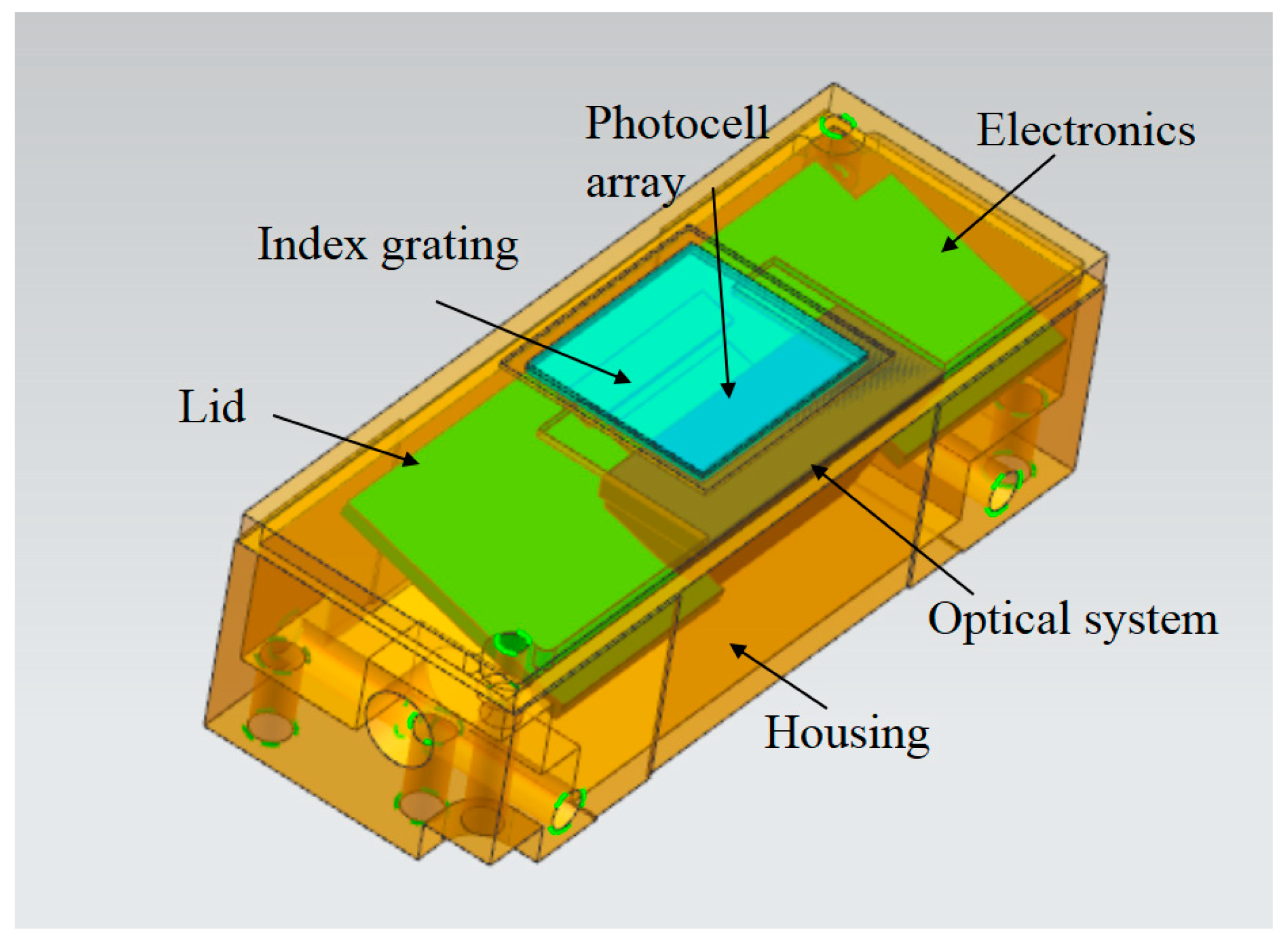
2.1. Working Principle of Open-Type Optical Linear Encoder

The operational framework of the open-type optical linear encoder is illustrated in Figure 2. This encoder consists of two integral components—the reading head and the main scale. The reading head includes the optical system, index grating, photocell array, and electronic system, while the main scale is made from graduated glass strips or reflective metal tapes. The optical system emits a collimated blue light source for the encoder, and the index grating—a combination of amplitude and phase grating—mitigates the Talbot effect. It has the same pitch period as the main scale, thereby enabling the generation of Moire fringes. The photocell array captures and converts optical signals into current signals. Transimpedance amplifiers [25] on the electronics system then transform current signals into electrical voltage signals. The final output sinusoidal signals are then processed by the interpolation box, or the servo drive, to acquire the TTL signal. The main scales, commonly made of graduated glass strip or reflective metal tapes, are typically fabricated by mask lithography, laser beam scanning [26], or nanoimprint [27] technologies. In the industrial realm, due to limitations in production costs and precision requirements, the most common pitch periods for main scales are 20 μm or 40 μm [28]. In particular, the pitch lines in this research are rectilinear.
The output sinusoidal signals can be represented by the following expression:
O s = V sin 2 π p d O c = V cos 2 π p d ,
where O s and O c signify the electrical output signals, V is the amplitude, p denotes the pitch period on the main scale, and d represents the measured displacement value, which can be calculated by Equation (2). The term of this calculation is referred to as interpolation or subdivision.
d = p 2 π arctan O s O c ; O s 0 , O c > 0 d = p 4 ; O s > 0 , O c = 0 d = p 2 p 2 π arctan O s O c ; O s 0 , O c < 0 d = p 2 + p 2 π arctan O s O c ; O s < 0 , O c < 0 d = 3 p 4 ; O s < 0 , O c = 0 d = p p 2 π arctan O s O c ; O s < 0 , O c > 0 .

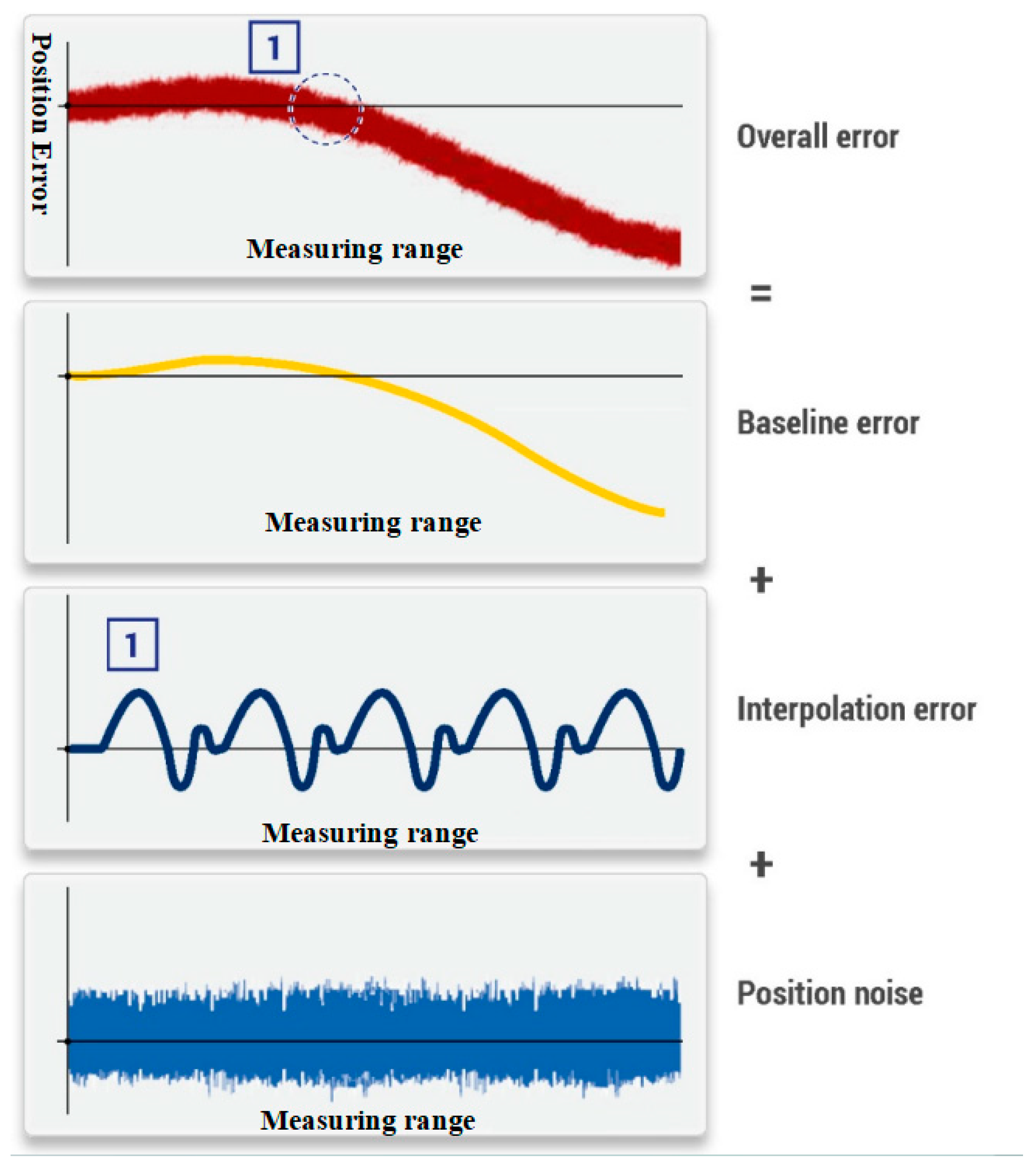
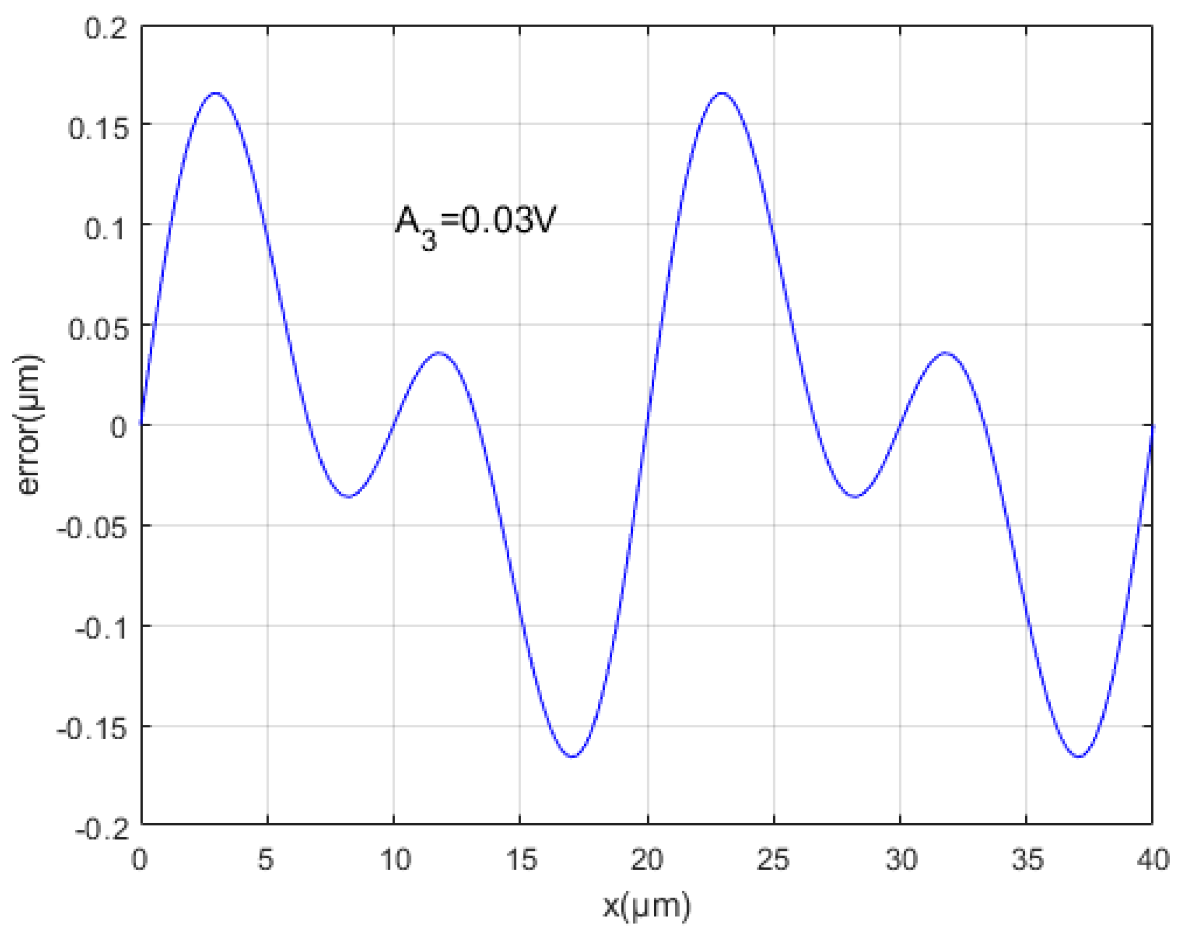
2.2. Theoretical Investigation for SDE Reduction

In real-life industrial scenarios, errors can be introduced by various factors. For instance, errors may arise from imperfect grating lines on the main scale and/or index grating, the angle errors between the grating pair due to installation or assembly issues, light source deviation or attenuation, mechanical defects, and so forth. Consequently, the output sinusoidal signals exhibit imperfections and can be expressed as:
O sreal = D 1 + i = 1 k V 1 i sin 2 n π p d + α i O c r e a l = D 2 + i = 1 k V 2 i cos 2 n π p d + β i .
Here, D 1 and D 2 represent the DC offsets, i signifies the harmonic order, k denotes the maximum number of harmonic orders, V 1 i and V 2 i are the amplitudes of the i th order of harmonic, while the angular deviations of the the i th order of harmonic can be expressed as α i , β i , respectively. DC offsets, harmonics, differences in amplitudes, and angular deviations constitute the primary factors causing interpolation errors. DC offsets can be relatively easy to calibrate using commercial ICs [29]. Hence, they will be disregarded in this study. Notably, the amplitude of higher-order harmonics significantly diminishes beyond the third order. As a result, harmonics from the fourth order onwards will not be considered in this calculation. With these considerations, the sinusoidal signals can be reformulated as follows:
O sreal = V 11 sin 2 π p d + α 1 + V 12 sin 4 π p d + α 2 + V 13 sin 6 π p d + α 3 O creal = V 21 cos 2 π p d + β 1 + V 22 cos 4 π p d + β 2 + V 23 cos 6 π p d + β 3 .
The photocell array generates four row signals in phases 0°, 90°, 180°, and 270°. Subtracting signals with a 180° angular difference eliminates the second order harmonic, further simplifying the equation as:
O sreal = V 11 sin 2 π p d + α 1 + V 13 sin 6 π p d + α 3 O creal = V 21 cos 2 π p d + β 1 + V 23 cos 6 π p d + β 3 .
The third order harmonic in Equation (3) leads to SDEs. Assuming V 11 = V 21 are both set to 1 V, while V 13 = V 23 = A 3 is assigned a value of 0.03 V, this means that the containment of the third order harmonic is 3% in the analog output of the optical linear encoder. With a pitch period of 40 μm, SDE can be calculated using Equation (5); the SDE curve is illustrated in Figure 3. In this scenario, the SDE within one pitch period is ±0.17 μm, solely caused by the third order harmonic without considering other factors.
To minimize the SDE value, it is imperative to suppress the signal distortion caused by the third order harmonic. In this research, the angle shift method is proposed, introducing an additional angle ω in Equation (5) and transforming it as follows:
O 1 sreal = V 11 sin 2 π p d + ω + α 1 + V 13 sin 6 π p d + ω + α 3 O 1 creal = V 21 cos 2 π p d + ω + β 1 + V 23 cos 6 π p d + ω + β 3 .
New equations can be derived by summing Equations (5) and (6):
O 2 sreal = 2 V 11 sin 2 π p d + ω 2 + α 1 cos π ω p + 2 V 13 sin 6 π p d + ω 2 + α 3 cos ( 3 π ω p ) O 2 creal = 2 V 21 cos 2 π p d + ω 2 + α 1 cos π ω p + 2 V 23 cos 6 π p d + ω 2 + α 3 cos ( 3 π ω p ) .
To eliminate the third order harmonic, the solution involves setting cos ( 3 π ω p ) to zero. In other words, 3 π ω p = 2 n + 1 2 π , where n is an integer. This research investigates the SDE, which represents the error within one pitch period. Hence, the actual limitation for angle shift is within the width of the pitch period. Therefore, only ω = p 6 or ω = p 6 can be selected in this scenario. Based on this reason, the pattern of the grating lines can be redesigned as shown in Figure 4b to suppress the third order harmonic. In comparison, the traditional grating lines are illustrated in Figure 4a.

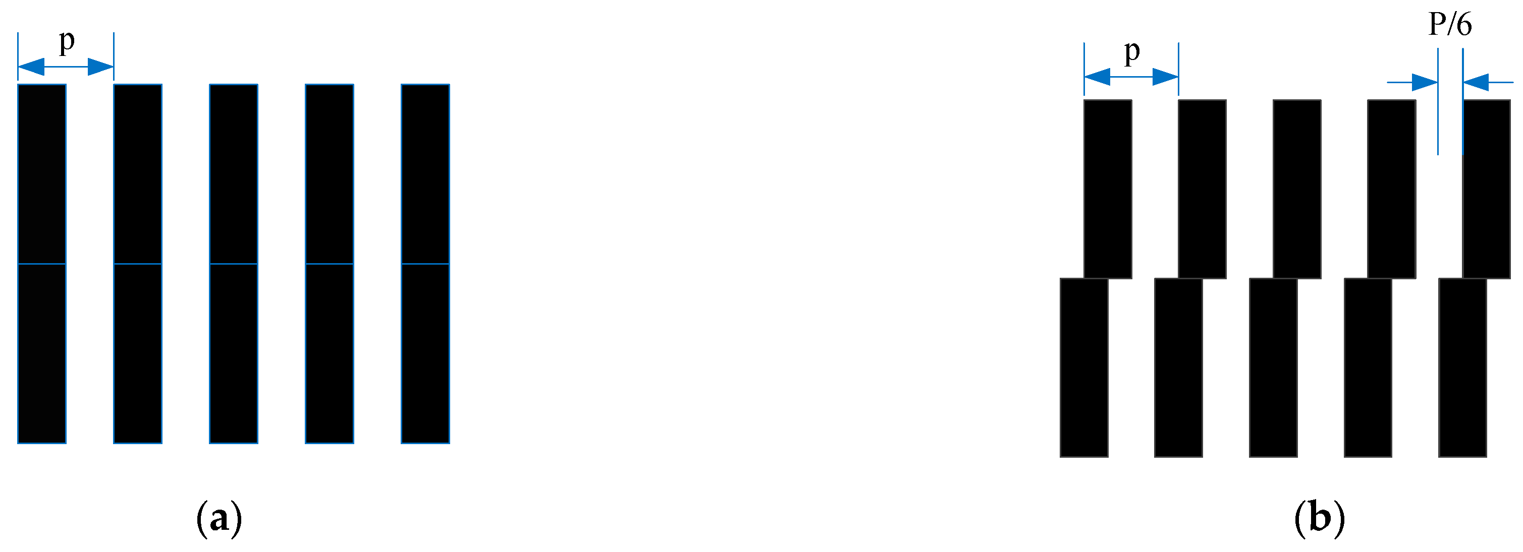
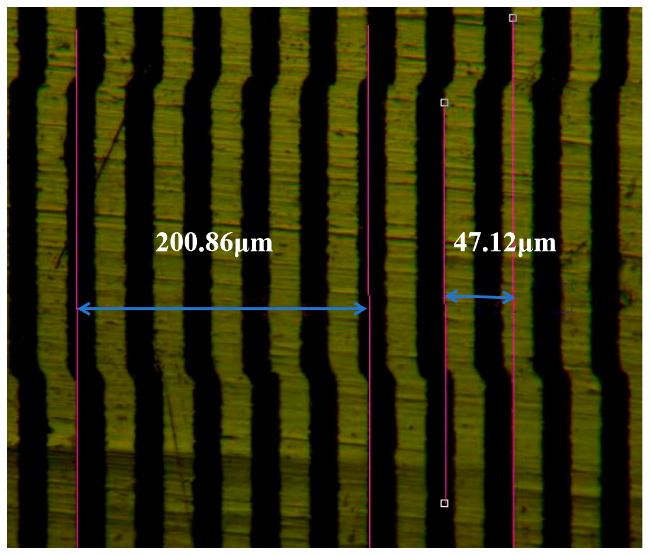
2.3. The Fabrication Method of the Proposed Main Scale

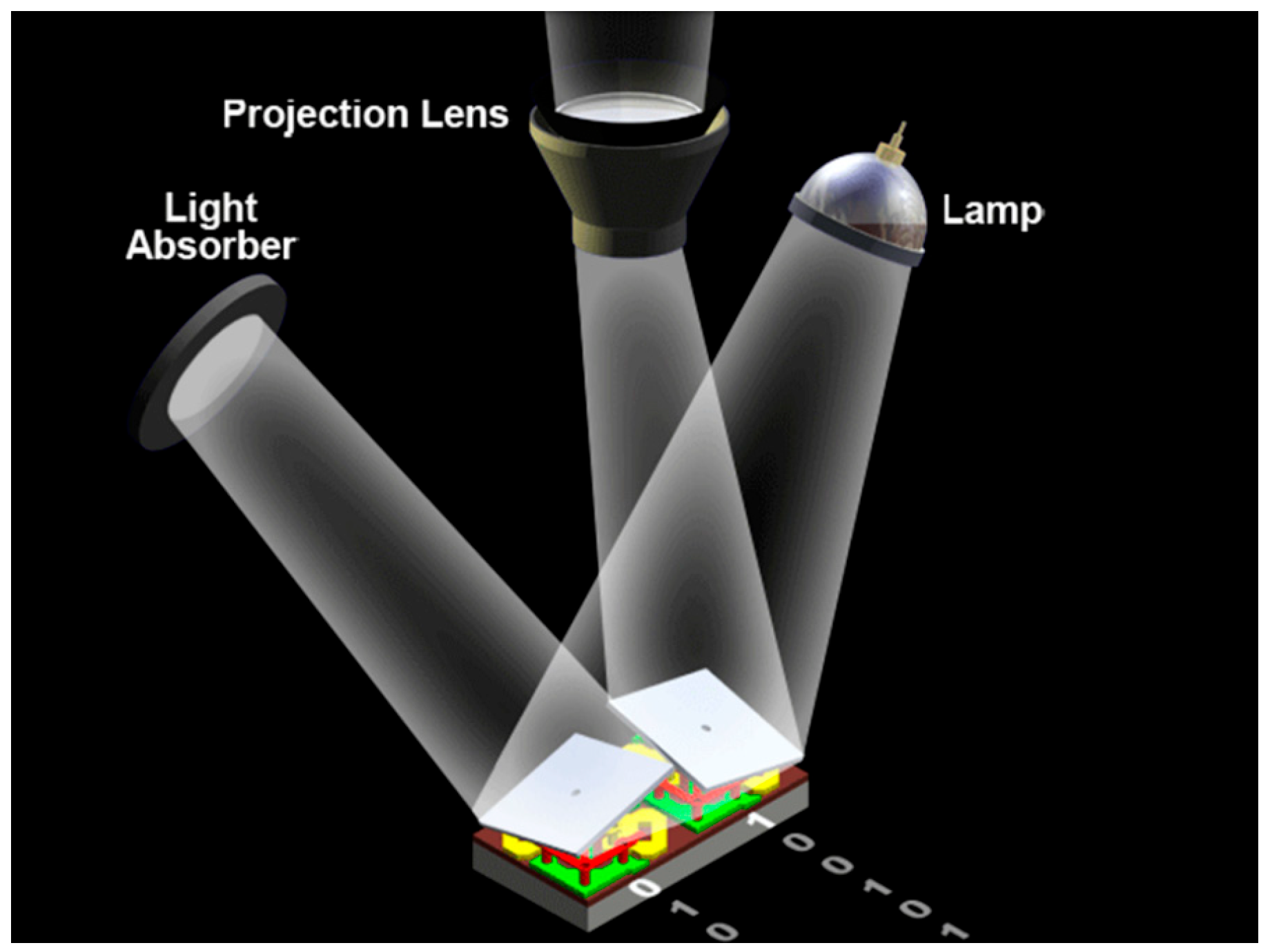
2.3.1. Maskless Lithography System

The methods discussed in Section 2.1 for fabricating main scales are suboptimal for producing the angle-shift pattern proposed in Section 2.2, especially for experimental purposes. Conventional techniques, which rely on molding or masks with pre-designed grating patterns, are both time-consuming and costly. Furthermore, once a mold or mask is created, the pattern on it becomes fixed, making minor revisions or modifications challenging without the fabrication of an entirely new replacement. To overcome these limitations, this experiment utilizes maskless lithography technology, also referred to as ‘virtual mask’ lithography technology. This technology utilizes the digital mirror device (DMD) from Texas Instruments, which consists of millions of micro-mirrors and is capable of generating image patterns. Each micro-mirror has only two fixed positions: +12° and −12°. As illustrated in Figure 5, when in the +12° position, the micro-mirror reflects light from the projection lens, illuminating a pixel. Conversely, in the −12° position, a dark pixel is generated [30]. Such two stage correspond to the digital ‘0’ and ‘1’, in this way, the computer program can generate any designed pattern by controlling the status of micro-mirrors on the DMD device.
The maskless lithography equipment comprises three parts: the exposure unit, the upper computer with control software, and a motion platform, as shown in Figure 6. The exposure unit comprises the 405 nm laser light source, the DMD device, electronics, and a focusing system. This unit can project the pattern of the virtual mask onto the main scale, and defocusing can be calibrated to determine the correctness of position as well. The motion platform encompasses the X, Y, and Z axes. The X-axis is affixed to the gantry’s crossbeam, the Y-axis is situated on the pedestal. The main scale moves along the Y-axis direction for exposure, advancing forward after completing one exposure area. Controlled by the upper computer, each pixel of the pattern synchronizes with the motion during exposure. Theoretically, this method can generate any 2D pattern; the maximum length of the main scale is only limited by the Y-axis’s travel range. Figure 6 illustrates the maskless lithography equipment.

2.3.2. The Process of Fabrication

The fabrication of the main scale involves several critical steps: metal surface brightening, coating, maskless lithography, development, and etching. Commencing with the metal surface brightening process, it is essential to ensure uniform reflection rates across all sections of the metal tape. This procedure ensures a consistent amplitude of analog signals from the optical linear encoder along the measurement length of the main scale. During the coating phase, meniscus-coating technology is employed. This technique utilizes a meniscus-shaped container where photoresist is injected. The metal tape travels past the container at a constant velocity, and the photoresist outflows from an ostiole situated at the top of container. Fine-tuning the velocity of the tape and the pressure in the container enables precise control of the coating thickness. The metal tape is attached to the motion platform of the maskless lithography equipment along the Y-axis. The proposed pattern is exposed onto the coating surface, and this lithography process continues until the entire measurement range of the main scale is exposed. The development stage involves the use of a developer to remove the photo-curing patterns from the coating surface. The subsequent etching process produces low-reflective patterns on the surface of metal tape. Figure 7 displays a sample of a main scale produced by this fabrication process. The total length of the first five pitch periods is 200.86 μm, indicating an average pitch period of 40.172 μm. The length of one angle shift distance and a pitch period is 47.12 μm, where ω = 6.948 μm, nearing the target value of 6.695 μm.

3. Experimental Setup

The schematic diagram of the open-type optical linear encoder’s reading head employed in this experiment is illustrated in Figure 8. The reading head comprises the optical system, electronic system, photocell array, index grating, housing, and lid. To ensure precise positioning of the light source and lens within the specified tolerance, the optical system is securely affixed to the holder. The index grating, fabricated on a glass substrate with chrome and TiO2 grating lines, forms a hybrid grating with a pitch period of 40 μm, matching the main scales used in this experiment. The photocell array is a specially designed integrated circuit (ASIC) following the principle of single-field scanning. This type of photocell presents advantages, as it is less susceptible to environmental pollutions such as dust, scratched grating lines, or fingerprints on the main scale. The electronic system processes the signals, while the housing and lid provide support and protection for all vital components. Threaded holes on the side facilitate convenient mounting.
To evaluate the error of an optical linear encoder, a common approach involves utilizing a displacement sensor or measurement equipment with higher grade of accuracy, such as a laser interferometer. However, challenges arise in ensuring the measurement trajectory precisely aligns or coincides with the actual travel path of the optical linear encoder. Despite the high measurement accuracy, even slight deviations or unevenness in the mounting surface of the main scale could introduce additional errors. Furthermore, conducting experiments aimed at collecting data from six different periods and gathering 1000 position points within each period using a laser interferometer could be time-consuming. During this duration, the inevitability of unwanted factors, such as vibration, electrical noise, or temperature fluctuations, increases, potentially introducing random errors to the experimental data.
Due to this consideration, the experiment employs the constant velocity method. The experimental components include:
  • Computer with control software;
  • ACS servo drive;
  • Planar XY linear stage;
  • Reading head and main scales;
  • IC-Haus SinCosYzer.
By utilizing control software SPiiPlus application studio 2.70, the computer issues commands to the ACS servo drive via the EtherCAT protocol, directing the Planar XY linear stage to execute constant-speed movement. Both the proposed and traditional main scales are secured to the optical bench using the special steel tape mounting tool to ensure the linearity. The reading head is connected to the planar XY linear stage via mounting brackets. The precise calibration of the reading head’s distance relative to the main scale is achieved through the utilization of spacers, ensuring an optimal working distance. Subsequently, the reading head is applied to evaluate two types of main scales, facilitating an analytical examination of the respective influences on the output. The IC-Haus SineCosYzer is employed to collect the analog signals generated by the reading head. The experimental setup is demonstrated in Figure 9.
As the SDEvalue is often deemed critical in low-velocity trajectory control applications, the test velocity is deliberately set at 0.1 m/s. The sinusoidal signals generated by the reading head were meticulously collected using a data acquisition card and were subsequently transmitted to a computer for analytical processing. Employing a sampling frequency of 2.5 MHz, each data step represents a precise interval of 0.04 μm. Considering the 40 μm pitch period of the tested optical linear encoder, a comprehensive dataset comprising 1000 position values was collected per period, from the initial position of 0 to the concluding position of 40 μm. For each type of the main scale, six periods of signal values were meticulously recorded separately.

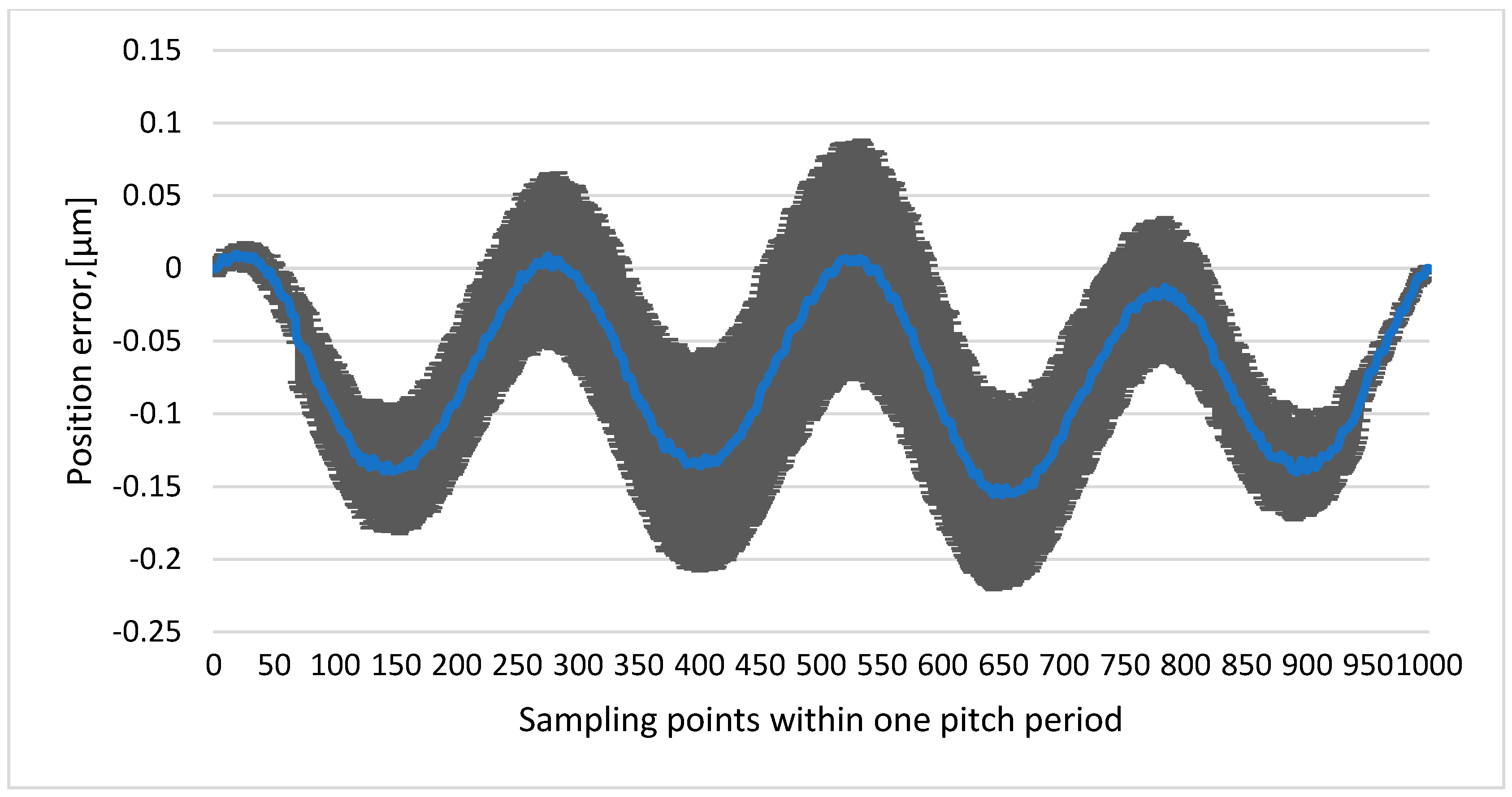
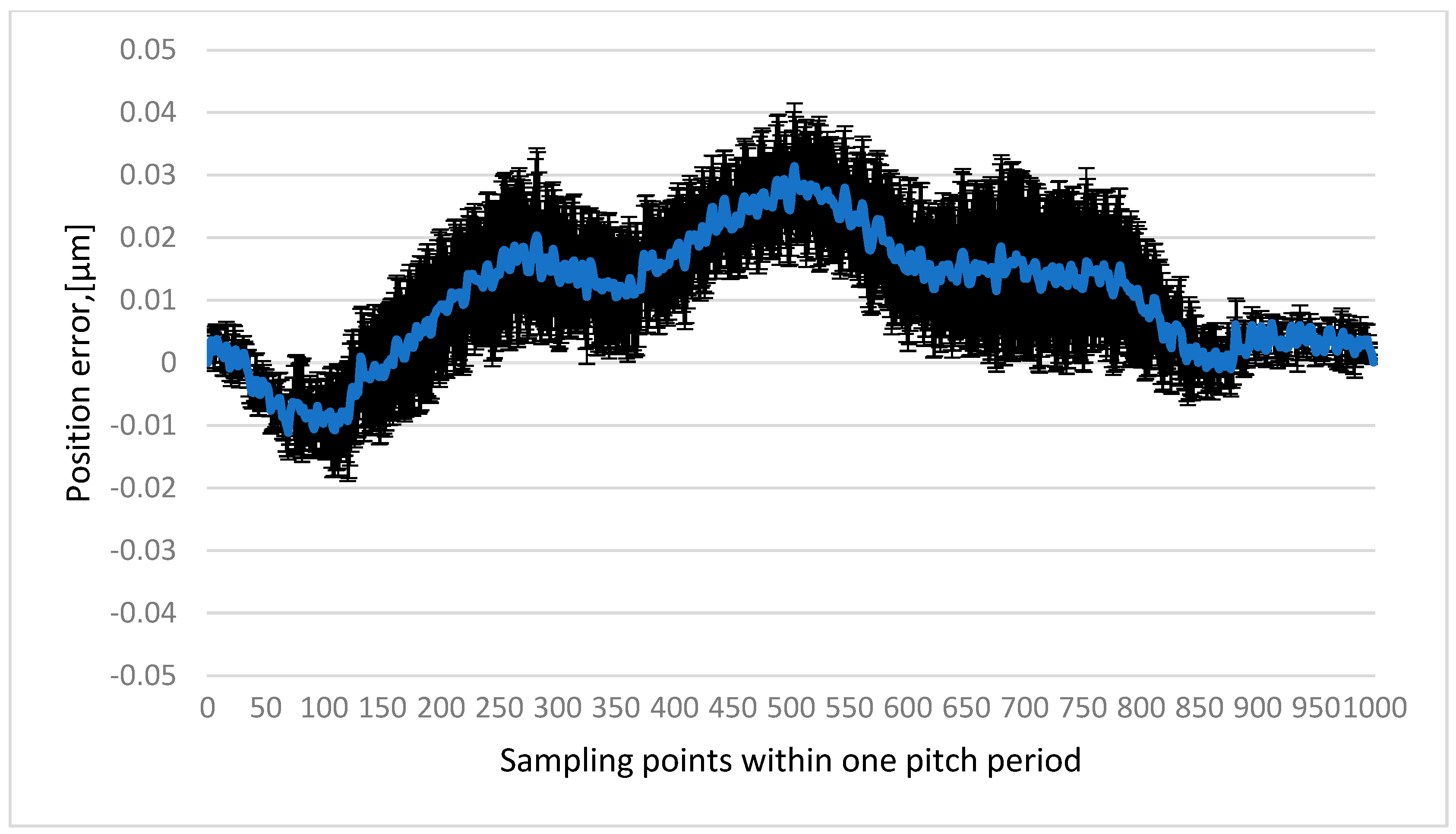
4. Experiment Results and Discussion

Analyzing the Lissajous figure is a widely used method for evaluating the quality of analog sinusoidal signals produced by optical linear encoders. An ideal analog sinusoidal signals results in a perfect circular Lissajous figure. However, uneven amplitudes, angle deviations, DC-offsets, and imperfections in sine wave shape introduce distortions to this circular pattern. Figure 10 illustrates the Lissajous figures generated by the two different types of main scales. The green dotted circle serves as the ideal reference, while the red line circle is plotted using experimental data. In Figure 10a, the Lissajous figure is generated by signals with traditional main scales, displaying a more distorted figure compared to the Lissajous figure generated with the proposed angle shift pattern main scale, as shown in Figure 10b.
The experimental results of the SDE are illustrated in Figure 11 and Figure 12. The Y-axis represents the position error value within one pitch period, while the X-axis denotes 1000 position points sampled within the distance of one pitch period. Given that the pitch period of both main scales is 40 μm, each step represents 0.04 μm. The blue lines in both figures represent the average values based on six sets of data collected from different pitch periods on the main scale, while the black lines are the error bars. As shown in Figure 11, the average SDE value for the traditional grating ranges from −0.156 to 0.01 μm, totaling 0.157 μm. In contrast, the proposed angle shift pattern main scale shows an average SDE value range of −0.01 to 0.03 μm, totaling 0.04 μm, as demonstrated in Figure 12. This suggests that the average SDE value of the traditional grating is 3.925 times higher than the main scale with the proposed angle shift pattern.
Within each examined pitch period, the quantification of the third order harmonics was undertaken through the application of the fast Fourier transformation (FFT) method. Table 1 reveals that, employing the traditional main scale, five out of the six examined pitch periods manifested the third order harmonics content exceeding 2%. In stark contrast with the incorporation of the proposed angle shift pattern main scale, only two out of the six examined pitch periods revealed third order harmonics content surpassing 0.1%. On average, the third order harmonic content with the proposed main scale amounts to 0.09%, whereas its traditional counterpart records a value of 2.07%. This signifies a noteworthy reduction of 95.65% in the third order harmonics with the adoption of the proposed methodology.
Based on the experimental results, the subsequent discussion focuses on key points and implications derived from the outcomes.
  • Correlation between harmonic suppression and SDE reduction: Under specific conditions where DC-offset, signal amplitudes, and orthogonality are carefully controlled, a notable correlation is observed. The successful suppression of the third order harmonic demonstrates a strong correlation with the reduction in SDE. This finding underscores the importance of harmonic control in achieving fine precision in optical linear encoders.
  • Significance of SDEs in achieving higher resolution: Beyond the established threshold of SDEs, the pursuit of increased resolution in an optical linear encoder becomes impractical. For advanced industrial applications, high-resolution demands often lead to the utilization of costly displacement sensors, such as laser interferometers. The method proposed in this research presents a promising avenue for developing ‘high-end’ displacement sensors at a more cost-effective scale, potentially benefiting precision equipment across various industries.
  • Challenges in practical industrial environments: In industrial environments, factors such as vibrations, electromagnetic interference, and temperature fluctuations are prevalent. These factors have the potential to significantly influence SDE, potentially undermining the accuracy of optical linear encoders. It is noteworthy that the SDE data presented in this investigation is obtained under controlled laboratory conditions. Subsequent research endeavors will explore the impact of real-world industrial factors on the efficacy of the proposed method, validating the robustness in practical applications. The investigation can contribute valuable insights into the method’s performance in diverse and challenging operational conditions.
  • The proposed DMD maskless lithography technology, while ideal for academic research and experimental purposes, may encounter challenges in mass-producing long-range main scales. The maximum exposure length of the main scale is constrained by the travel range of the motion platform. The implementation of long-range fabrication requires a costly motion platform. A cost-effective strategy involves using DMD maskless lithography technology to create masks, combining them with high-precision probes to extend the mask’s range. Subsequently, the contact exposure approach can be applied for the mass production of long-range main scales.
  • The potential applicability of the proposed method extends to other types of optical encoder, such as the enclosed-type optical linear encoder and the open-ring-type angular encoder to reduce SDEs. In the case of enclosed-type optical linear encoders, the inclusion of additional phase lines on the index grating is unnecessary, as mechanical systems ensure a fixed distance between the index grating and the main grating. Consequently, it is more convenient to implement the suggested patterns on the index grating rather than on the main scale.

5. Conclusions

In conclusion, this study presents a novel angle-shift method to effectively reduce SDEs in open-type optical linear encoders. The research investigates the theoretical foundations of harmonic suppression and introduces a distinctive approach using specially designed angle-shifted patterns on the main scale. The experimental results demonstrate a notable correlation between the effective suppression of the third order harmonic and the reduction in SDEs. Furthermore, the study highlights the critical role of SDEs in limiting the achievable resolution of optical linear encoders, emphasizing its significance in precision instrumentation. The proposed method demonstrates promising potential to offer a cost-effective alternative for fabricating high-end displacement sensors. Although this research provides valuable insights within a controlled laboratory environment, future investigations should extend to practical industrial conditions. In addition, ongoing research efforts should focus on refining the experimental methodologies, ensuring reproducibility and further validating the proposed approach in diverse applications. Essentially, this research contributes to the progress of optical linear encoder technology, presenting a compelling method for the reduction of SDEs.

Author Contributions

Conceptualization, X.L.; methodology, X.L.; software, F.Y.; validation, X.L. and A.K.; formal analysis, X.L.; investigation, X.L. and F.Y.; resources, F.Y. and A.K.; writing—original draft preparation, X.L.; writing—review and editing, X.L. and A.K.; supervision, F.Y. and A.K.; project administration, F.Y. and A.K. All authors have read and agreed to the published version of the manuscript.

Funding

This research received no external funding.

Data Availability Statement

The data presented in this study are available on request from the corresponding author. The data are not publicly available due to commercial reasons.

Conflicts of Interest

The authors declare no conflicts of interest.

References

  1. Peng, K.; Yu, Z.; Liu, X.; Chen, Z.; Pu, H. Features of Capacitive Displacement Sensing That Provide High-Accuracy Measurements with Reduced Manufacturing Precision. IEEE Trans. Ind. Electron. 2017, 64, 7377–7386. [Google Scholar] [CrossRef]
  2. Das, S.; Sarkar, T.S. A New Method of Linear Displacement Measurement Utilizing Grayscale Image. IJEEE 2013, 1, 176–181. [Google Scholar] [CrossRef]
  3. Miyajima, H.; Yamamoto, E.; Yanagisawa, K. Optical Micro Encoder with Sub-Micron Resolution Using a VCSEL. Sens. Actuators A Phys. 1998, 71, 213–218. [Google Scholar] [CrossRef]
  4. Seybold, J.; Bülau, A.; Fritz, K.-P.; Frank, A.; Scherjon, C.; Burghartz, J.; Zimmermann, A. Miniaturized Optical Encoder with Micro Structured Encoder Disc. Appl. Sci. 2019, 9, 452. [Google Scholar] [CrossRef]
  5. Engelhardt, K.; Seitz, P. High-Resolution Optical Position Encoder with Large Mounting Tolerances. Appl. Opt. 1997, 36, 2912. [Google Scholar] [CrossRef] [PubMed]
  6. Moers, A.J.M.; van Riel, M.C.; Bos, E.J. Design and Verification of the TriNano Ultra Precision CMM; Ilmenau University Library: Ilmenau, Germany, 2011. [Google Scholar]
  7. Cerón Viveros, M.F.; Rojas Arciniegas, A.J. Development of a Closed-Loop Control System for the Movements of the Extruder and Platform of a FDM 3D Printing System. NIP Digit. Fabr. Conf. 2018, 2018, 176–181. [Google Scholar] [CrossRef]
  8. Shin, B.; Jeon, S.; Lee, J.; Han, C.S.; Im, C.M.; Kwon, H.-J. Controlled Trigger and Image Restoration for High Speed Probe Card Analysis. Int. J. Precis. Eng. Manuf. 2015, 16, 661–667. [Google Scholar] [CrossRef]
  9. Mishra, S.; Coaplen, J.; Tomizuka, M. Precision Positioning of Wafer Scanners Segmented Iterative Learning Control for Nonrepetitive Disturbances [Applications of Control]. IEEE Control. Syst. 2007, 27, 20–25. [Google Scholar]
  10. Position Control in Lithographic Equipment [Applications of Control]. IEEE Control Syst. 2011, 31, 28–47. [CrossRef]
  11. Available online: https://www.rsf.at/wp-content/uploads/downloads/MS_25-EN.pdf (accessed on 20 January 2024).
  12. Qiao, D.; Xu, Z.; Wu, H.; Zeng, Q.; Liu, Y.; Sun, Q. A Method for Compensating Interpolation Error of Absolute Linear Encoder. Acta Opt. Sin. 2015, 35, 0112008. [Google Scholar] [CrossRef]
  13. Haitjema, H. The Calibration of Displacement Sensors. Sensors 2020, 20, 584. [Google Scholar] [CrossRef]
  14. Balemi, S. Automatic Calibration of Sinusoidal Encoder Signals. IFAC Proc. Vol. 2005, 38, 68–73. [Google Scholar] [CrossRef]
  15. Požar, T.; Gregorčič, P.; Možina, J. A Precise and Wide-Dynamic-Range Displacement-Measuring Homodyne Quadrature Laser Interferometer. Appl. Phys. B 2011, 105, 575–582. [Google Scholar] [CrossRef]
  16. Tan, K.K.; Tang, K.-Z. Adaptive Online Correction and Interpolation of Quadrature Encoder Signals Using Radial Basis Functions. IEEE Trans. Contr. Syst. Technol. 2005, 13, 370–377. [Google Scholar] [CrossRef]
  17. Dhar, V.K.; Tickoo, A.K.; Kaul, S.K.; Koul, R.; Dubey, B.P. Artificial Neural Network-Based Error Compensation Procedure for Low-Cost Encoders. Meas. Sci. Technol. 2010, 21, 015112. [Google Scholar] [CrossRef]
  18. Kavanagh, R.C. Probabilistic Learning Technique for Improved Accuracy of Sinusoidal Encoders. IEEE Trans. Ind. Electron. 2001, 48, 673–681. [Google Scholar] [CrossRef]
  19. Ye, G.; Liu, H.; Wang, Y.; Lei, B.; Shi, Y.; Yin, L.; Lu, B. Ratiometric-Linearization-Based High-Precision Electronic Interpolator for Sinusoidal Optical Encoders. IEEE Trans. Ind. Electron. 2018, 65, 8224–8231. [Google Scholar] [CrossRef]
  20. Tan, K.; Zhou, H.X.; Lee, T.H. New Interpolation Method for Quadrature Encoder Signals. IEEE Trans. Instrum. Meas. 2002, 51, 1073–1079. [Google Scholar] [CrossRef]
  21. Hane, K.; Endo, T.; Ito, Y.; Sasaki, M. A Compact Optical Encoder with Micromachined Photodetector. J. Opt. A Pure Appl. Opt. 2001, 3, 191–195. [Google Scholar] [CrossRef]
  22. Ieki, A.; Hane, K.; Yoshizawa, T.; Matsui, K.; Nashiki, M. Optical Encoder Using a Slit-Width-Modulated Grating. J. Mod. Opt. 1999, 46, 1–14. [Google Scholar] [CrossRef]
  23. Yang, F.; Lu, X.; Kilikevičius, A.; Gurauskis, D. Methods for Reducing Subdivision Error within One Signal Period of Single-Field Scanning Absolute Linear Encoder. Sensors 2023, 23, 865. [Google Scholar] [CrossRef]
  24. Lu, X.; Kilikevičius, A.; Yang, F.; Gurauskis, D. A Method to Improve Mounting Tolerance of Open-Type Optical Linear Encoder. Sensors 2023, 23, 1987. [Google Scholar] [CrossRef]
  25. Rozman, J.; Pletersek, A. Linear Optical Encoder System with Sinusoidal Signal Distortion Below −60 dB. IEEE Trans. Instrum. Meas. 2010, 59, 1544–1549. [Google Scholar] [CrossRef]
  26. Fursenko, A.; Kilikevičius, A.; Kilikevičienė, K.; Borodinas, S.; Kasparaitis, A.; Gurauskis, D. Experimental Investigation of Friction Transition on Vibration of Steel Tapes. In AIP Conference Proceedings, Yogyakarta, Indonesia, 29 October 2018; AIP Publishing: College Park, MA, USA, 2018; p. 020016. [Google Scholar]
  27. Merino, S.; Retolaza, A.; Juarros, A.; Landis, S. A New Way of Manufacturing High Resolution Optical Encoders by Nanoimprint Lithography. Microelectron. Eng. 2007, 84, 848–852. [Google Scholar] [CrossRef]
  28. Goudarzi Khouygani, M.H.; Jeng, J.-Y. High-Precision Miniaturized Low-Cost Reflective Grating Laser Encoder with Nanometric Accuracy. Appl. Opt. 2020, 59, 5764. [Google Scholar] [CrossRef] [PubMed]
  29. Pletersek, A.; Benkovic, R.; Trontelj, J. Interpolation Method and Frequency Independent Peak Amplitude Measurement of Orthogonal—Periodic Signals. Recent Pat. Eng. 2011, 5, 82–93. [Google Scholar] [CrossRef]
  30. Lee, B. Introduction to ±12 Degree Orthogonal Digital Micromirror Devices (DMDs); Texas Instruments: Dallas, TX, USA, 2008. [Google Scholar]
Figure 1. The composition of errors of the optical linear encoder (www.rsf.at).
Mathematics 12 00474 g001
Figure 2. Working principle of open-type optical linear encoder.
Mathematics 12 00474 g002
Figure 3. The SDE curve when the third order harmonic is 3% in the output signal.
Mathematics 12 00474 g003
Figure 4. The pattern of the main scales: (a) the traditional pattern; (b) the proposed pattern with the angle shift method to suppress the third order harmonic.
Mathematics 12 00474 g004
Figure 5. The working principle of the DMD device (www.ti.com).
Mathematics 12 00474 g005
Figure 6. The maskless lithography equipment.
Mathematics 12 00474 g006
Figure 7. The main scale with the proposed angle shift pattern.
Mathematics 12 00474 g007
Figure 8. Schematic diagram of the open-type optical linear encoder’s reading head.
Mathematics 12 00474 g008
Figure 9. Schematic of the open-type optical linear encoder’s reading head.
Mathematics 12 00474 g009
Figure 10. The Lissajous figures: (a) Lissajous figure generated with data from traditional main scale; (b) Lissajous figure generated with data from proposed angle shift pattern main scale.
Mathematics 12 00474 g010
Figure 11. Average SDE curve with error bars when main scale with traditional pattern on surface is employed.
Mathematics 12 00474 g011
Figure 12. Average SDE curve with error bars when main scale with proposed angle shift pattern on surface is employed.
Mathematics 12 00474 g012
Table 1. The content of third order harmonics with different types of main scales.
Main ScalesTraditional Main ScaleProposed Main Scale
The content of third order harmonics in 6 examined pitch periods2.27%0.13%
1.58%0.09%
2.31%0.04%
2.18%0.08%
2.07%0.12%
2.00%0.05%
Average value2.07%0.09%
Disclaimer/Publisher’s Note: The statements, opinions and data contained in all publications are solely those of the individual author(s) and contributor(s) and not of MDPI and/or the editor(s). MDPI and/or the editor(s) disclaim responsibility for any injury to people or property resulting from any ideas, methods, instructions or products referred to in the content.

