Abstract
This paper presents the results of studying the characteristics of hydrogen sensors based on thin In2O3 films modified with tin and dysprosium with dispersed double Pt/Pd catalysts deposited on the surface. To control the content of Sn and Dy in the films, an original technology was developed, and ceramic targets were fabricated from powders of the In–Dy–O, Dy–Sn–O, and In–Dy–Sn–O systems synthesized by the sol–gel method. Films of complex composition were obtained by RF magnetron sputtering of the corresponding targets. Structural features of the obtained thin films were studied by Raman spectroscopy. It is shown that various combinations of tin and dysprosium concentrations, as well as the presence of Pt/Pd catalysts on the surface, have a significant effect on the defectiveness of the films and the density of oxygen adsorption centers. As a result, the resistance of sensors in pure air (R0), the activation energies of the temperature dependences of R0, the bending of the energy bands at the grain boundaries of the semiconductor, and the responses to the action of hydrogen in the concentration range of 20–25,000 ppm change. A unique feature of Pt/Pd/ In2O3: Sn (0.5 at%), Dy (4.95 at%) films is their high sensitivity at 20–100 ppm and the absence of signal saturation in the region of high hydrogen concentrations of 5000–25,000 ppm, allowing them to be used to detect H2 in a wide range of concentrations.
1. Introduction
Since the 1960s, transparent conducting oxides have been widely used for optoelectronic applications [1,2,3]. Tin-doped indium oxide (ITO) is one of the most important transparent conductive oxides for such applications. To date, ITO has the best combination of characteristics in terms of electrical conductivity and optical transmission. Low resistance (about 1–2 × 10⁻⁴ Ω∙cm) and a high concentration of charge carriers (about 1 × 1020 cm–3), together with high transparency in the visible range (about 90%) [4], make it possible to widely use ITO in photovoltaics and solar cells, spintronics, electrochromic devices, OLED and LSD displays, touch screens, biosensors, transparent heaters, and chemoresistive gas sensors [5,6,7].
The technology for producing ITO films is well developed. The films are stable, reproducible, and have good surface morphology. Therefore, ITO is an attractive material for creating new materials on its basis and expanding the field of application. Films based on indium oxide are promising for resistive gas sensors. To create high-speed, highly sensitive sensors with low power consumption and high stability of parameters during operation, it is necessary to introduce catalytic additives into the volume and deposit them onto the surface. The effectiveness of such an approach was demonstrated experimentally in a number of studies conducted on films with thicknesses >500–1000 nm obtained by thick-film technologies modified with oxides of transition metals [8,9,10,11,12,13] and Dy [14]. In [14], 5% Dy3+ doped In2O3 nanoparticles were prepared by the hydrolysis-assisted co-precipitation method, using dysprosium nitrate. X-ray diffraction (XRD) revealed that the synthesized nanoparticles have a cubic bixbyite phase and that the addition of Dy3+ as a dopant noticeably enhanced the sensing response of In2O3 to ethanol.
The published information on the properties of structures based on SnO2 with rare earth elements (PEEs) is also limited and usually refers to samples obtained by using thick-film technology [15,16,17,18,19]. The introduction of the rare earth elements Nb, Ce, La, Y, and Dy or their oxides during the synthesis of SnO2 films was used to control the crystallite size and gas-sensitive properties of sensors. As a rule, no phases of oxides of REEs are detected in the films. During thermal annealing, additives segregate on the surface of microcrystals in the form of ions, such as Y3+, Dy3+, etc.
The industrial production of gas sensors requires the development of a technology that includes the magnetron sputtering of targets of complex composition to obtain thin-film sensors with additives of noble, 3d, and rare earth metals. In combination with microelectronic technology in one technological cycle, it is possible to obtain a large number of miniature sensitive elements with identical characteristics. In the patent [20], Kazuyoshi Inoue et al. state that the introduction of one of the lanthanides (La, Nb, Sm, Eu, Gd, Dy, Ho, Er, Tm, Yb, and Lu) into the In2O3 film, which is part of the TFT field-effect transistors, allows us to control the characteristics of the device through a smooth change in the film conductivity and free charge carriers’ mobility and also to stabilize the device parameters. The oxide semiconductor film obtained in [20] by the DC sputtering method contained indium and at least one of the following elements: gadolinium, dysprosium, holmium, erbium, and ytterbium. The X-ray diffraction of the film showed only a peak obtained from a compound of bixbyite structure.
Previously, we carried out detailed research aimed at the developing an original technology for producing gas sensors by DC sputtering of mosaic metal targets in oxygen-argon plasma in an A 500 (Edwards) magnetron. The doping additives were applied to the surface of the targets. The theory and mechanisms of operation of sensors based on SnO2 and WO3 thin films with various catalysts in the bulk (Pt, Au, Ni, Co, Y, and Sc) and on the surface (Pt, Pd, and Au) were developed [21,22,23,24,25]. The paper [21] presents the results of an investigation of the nanostructure, element, and phase composition of thin (100–140 nm) tin dioxide films containing Ag, Y, Sc, Ag + Y, and Ag + Sc additives in the bulk and catalytic Pt/Pd clusters on the surface. The methods of atomic-force microscopy (AFM), scanning Auger microprobe equipped with an Ar+ ions sputtering system (AES), and X-ray photoelectron spectroscopy (XPS) were used. Sensors based on Pt/Pd/SnO2: Sb, Ag, Y films were characterized by ultrahigh response values at 50–1000 ppm of H2 and the stabilization of parameters during long-term tests. The mechanisms of the influence of PEE impurities on the characteristics of thin films of tin dioxide are considered.
In this work, the structural, electrophysical, and gas-sensing properties of thin (about 100 nm) In2O3 films were studied. The films were obtained via the RF magnetron sputtering of specially designed original oxide targets with various contents of tin and dysprosium. The dispersed Pt and Pd catalysts were deposited on the surface of the targets. Raman spectroscopy was used to characterize the nanosized films. This is the only method to analyze thin films directly in the miniature sensors. It provides important information about film defects. The Raman spectra of bulk materials differ greatly from those of polycrystalline samples, where the size of particles (grains, agglomerates, clusters, etc.) lies in the nanometer range and the classical modes shift and expand. Doping with impurities and the deposition of dispersed catalyst clusters on the film surface can lead to the appearance of additional peaks and a change in the shape of the spectrum. Of particular interest is the prospect of creating semiconductor sensors for high pre-explosive concentrations of hydrogen that are not available on the market.
2. Materials and Methods
Ceramic targets (CTs) were fabricated by uniaxial static pressing of In2O3, SnO2, and Dy2O3 powder compacts on a PLG 12 hydraulic press (LabTools, Saint Petersburg, Russia) at a pressure of 1500 atmospheres. The targets were sintered in a muffle furnace in an air atmosphere at 1000 °C for 1 h. When obtaining powders for compaction, a chemical method was used based on the co-deposition of metal hydroxides by neutralizing solutions of their salts with an alkaline agent, washing of the obtained precipitation of hydroxides, filtering them, drying, and thermal destruction. All reagents were of special-purity grade. The application of this method to obtain powders of mixed oxides of indium, tin, and dysprosium is described in [26].
The targets were 75 mm in diameter and 6 mm thick. The 150 µm thick sapphire plates were used as the substrates. The deposition of thin films of modified In2O3 was carried out by RF magnetron sputtering in an A-500 magnetron (Edwards, Burgess Hill, UK) at a discharge power of 100 W. The working gas contained 56 ± 0.5 vol.% of oxygen, and the rest was argon. The pressure in the chamber was within (6.5 – 7) × 10−3 mBar. The target-substrate distance was 90 mm. For 100 nm thick films, the sputtering time was 30 min. Two-layer Pt/Pd catalysts were deposited on the surface of the films by DC magnetron sputtering. First palladium was deposited and then platinum was deposited (each layer was deposited for 15 s).
Contacts to the sensitive In2O3 layers (Figure 1a) and a heater on the reverse side of the substrate (Figure 1b) were formed via the sputtering of platinum, followed by photolithographic engraving prior to the deposition of semiconductor films. After the formation of the films, the finished samples were subjected to technological annealing in air at a temperature of 720 K for 24 h. Up to 500 sensors were obtained on one substrate with a diameter of 30 mm. Then the samples were cut into individual elements, 0.7 × 0.7 mm in size (sensitive area of 0.3 × 0.3 mm2), and gold electrical wires measuring 50 μm in diameter were welded to the contact pads of the sensors by thermal compression. Next, the sensors were assembled into TO-8 cases (Figure 1c).
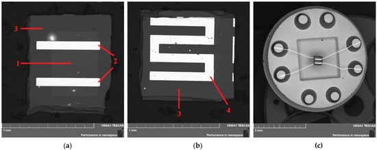
Figure 1.
SEM images obtained in the backscattering (BSE) mode: the sensitive element from the side of (a) semiconductor SnO2 layer and (b) heater. Sensors assembled into TO-8 cases (c): 1—sensitive layer; 2—Pt electrodes; 3—sapphire substrate; and 4—Pt heater.
Let us introduce the following numbering and notations for films of various compositions:
(I) In2O3 (90 at%): Sn (10 at%).
(II) Pt/Pd/In2O3 (90 at%): Sn (10 at%).
(III) Pt/Pd/In2O3 (86 at%): Sn (10 at%), Dy (4 at%).
(IV) Pt/Pd/In2O3 (94.05 at%): Sn (1 at%), Dy (4.95 at%).
(V) Pt/Pd/In2O3 (94.55 at%): Sn (0.5 at%), Dy (4.95 at%).
(VI) Pt/Pd/In2O3 (97 at%): Sn (1 at%), Dy (2 at%).
The Raman spectra of the films were measured on an inVia Basic confocal Raman spectrometer (Renishaw, Wotton-under-Edge, UK), operating in the backscattering mode at room temperature. The laser excitation wavelength was 785 nm (details of the research technique are presented in [23,24]).
To determine the sensor characteristics, the resistance (R0) and conductivity (G0) of the films were measured in pure air. The values of R1(G1) were also measured under various hydrogen concentrations, depending on the operating temperature in the constant and pulsed heating modes. The relative humidity in the chamber was maintained at the level of RH = 35%. The ratio of conductivities, G1/G0, was taken as the adsorption response to hydrogen. The settling time of 0.9 Gst, where Gst is the stationary value of the conductivity, was taken as the response time, tr. Based on the time dependences of the conductivity of sensors in the thermal cycling mode in pure air, the values of the energy band bending, eφs, at the grain boundaries in the studied nanocrystalline films were measured by using the method developed in [25]. The measuring stand and measurement techniques are described in [22]. The principle of operation and the theory of thin-film gas sensors are presented in [22,23,24,25].
3. Results and Discussion
3.1. Raman Spectra of Pt/Pd/In2O3: Sn, Dy Films of Various Compositions
The crystallographic structure of In2O3 belongs to the cubic system, the structure of bixbyite [27,28]. A complete description and identification of the Raman spectrum, even for undoped In2O3, is still being researched. At room temperature, no more than 10 modes can be observed, with all peaks in the range of 100–650 cm–1 [27,28,29,30]. In most cases, the following peaks are present in the Raman spectra of In2O3: 109, 132, 307, 366, 497, 517, and 630 cm−1. These are approximate values since their positions vary depending on the methods of obtaining the metal oxide and the measurement technique.
Figure 2 shows the Raman spectra of all compositions of the obtained films, as well as the spectra of SnO2 and In2O3 powders. The spectra of the powders, in principle, only slightly differ from those given in the literature for coarse-grained samples (bixbyite structure) [27,28,29,30]. In the case of In2O3 modified with Sn and Dy, broad bands with a number of maxima are observed in the range of 200–800 cm–1. Similar bands observed for many nanostructured metal oxide films are attributed to dimensional effects [30,31,32,33]. The intensities of all modes are higher for films of Composition (V) containing 4.95 at% dysprosium. The low-frequency Ag modes appear as broadened bands at 100–170 cm–1, with a maximum-intensity peak at 119 cm–1, as well as a peak at 299 cm–1 shifted by 8 cm–1 relative to 307 cm–1. Two modes, F2g at 213 and 366 cm–1, are most noticeable for the samples of Composition (VI). The intense peak at 630 cm–1 inherent in indium and tin oxides (visible in the spectra of the corresponding powders) is weakly manifested only in the spectrum of samples from Series (VI) with a reduced content of Dy (2 at%) and a higher Sn content (1 at%).

Figure 2.
Raman spectra of obtained films and powders.
A feature of the Raman spectra of the studied films is the presence of high-frequency, low-intensity peaks at 565 and 590 cm–1, as well as a strongly pronounced peak at 648 cm−1 having the highest intensity for films from Series (III) to (V). These three peaks are not typical of In2O3. Previously [23,24], we showed that the Raman spectra of thin films of tin dioxide with dispersed Pt/Pd catalytic layers deposited on the surface also exhibit maxima at 565 and 590 cm–1. Upon the introduction of 13–14 at% Pt into the bulk of SnO2, the Raman spectra show an intense peak with a maximum at 590 cm–1 [23]. A detailed analysis of the experimental data showed that two states of platinum are present in tin dioxide: three-dimensional particles of metallic Pt0, which is not active in the Raman spectra, and an intermediate oxide PtO. This oxide is identified as two-dimensional dispersed platinum in the Pt2+ state responsible for the maximum at 590 cm−1. The maximum at 565 cm–1 corresponds to the similar state of Pd2+. The intense peak at 648 cm–1, the broadening of the low-frequency band, and the shift of the maximum to 119 cm–1 are apparently due to the presence of dysprosium.
According to [34], REEs are characterized by higher energies of breaking the bonds with oxygen compared to tin and indium: ΔHo298 = 171 kcal/mol for Y–O, ΔHo298 = 161 kcal/mol for Sc–O, ΔHo298 = 144 kcal/mol for Dy–O, ΔHo298 = 76 kcal/mol for In–O, and ΔHo298 = 127 kcal/mol for Sn–O. It was suggested [21] that during heat treatment of the tin dioxide thin films obtained by magnetron sputtering, yttrium and scandium atoms segregate on the surface of microcrystals, form strong bonds with the lattice oxygen, and are present in the form of Y+3 and Sc+3 ions. Similar phenomena can also take place under the modification of indium oxide with dysprosium. As a result of formation of a bond of Dy with lattice oxygen, the surface density of superstoichiometric indium and, possibly, tin atoms, which are centers of oxygen chemisorption, increases. The REE impurity ions can serve as catalysts on the surface of microcrystals to create additional active centers and increase sensitivity to hydrogen [21], ethanol [14], methanol [15], and acetone [18].
3.2. Electrical and Gas-Sensitive Properties of Sensors
Oxygen chemisorption occurs on the surface of the indium oxide thin films in the atmosphere. In the near-surface layer of the semiconductor, a space charge region (SCR) of width d0 depleted by electrons is formed, and the film conductivity decreases. During the dissociative adsorption of hydrogen on the surface of a thin-film sensor based on In2O3, atomic hydrogen interacts with a pre-chemisorbed oxygen ion, . The reaction product is water, which is desorbed from the surface, and the electron returns to the conduction band of the semiconductor. The conductivity of the sensor increases. The response value, G1/G0, is determined by the density of oxygen adsorption centers, Ni. The centers of adsorption are superstoichiometric atoms of indium and other metals present on the surface [22]. An important role is played by the nanocrystalline structure and the ratio between the doubled SCR width, 2d0, and the thickness of the films (or conduction bridges, dB).
An analysis of the experimental data shows that the characteristics of the studied films depend significantly on the ratio of the Sn and Dy concentrations in the bulk and the presence of Pt/Pd catalysts on the surface. Sn4+ ions substitute In3+ ones in the bulk and are donor impurities. As a result, the resistance of films of Composition (I) containing 10 at% Sn in pure air is R0 = 0.11 kΩ (Table 1). The deposition of dispersed Pt/Pd catalysts in the case of samples of Composition (II) promotes the active adsorption of oxygen in the form of on the surface and some increase in the SCR width and R0. The introduction of a Dy impurity (Composition (III)) into the bulk of In2O3 leads to a further increase in R0. The maximum values of R0 are observed for the sensors of Compositions (IV) and (V), in which the Sn concentration is reduced to 0.5–1 at% and the Dy content is 4.95 at%. A decrease in the concentration of dysprosium to 2 at% (Composition (VI)) contributes to the decrease in R0. The effect of the dysprosium impurity on the resistance of the films agrees with the features of the Raman spectra and confirms the assumption about the formation of strong bonds between Dy+3 ions and lattice oxygen. In this case, the density of chemisorbed oxygen on the film surface increases, and this contributes to the increase of the SCR width and resistance, R0.

Table 1.
Sensor resistances in pure air (R0) measured at 300 K; activation energies ∆E1 and ∆E2 of temperature dependences of R0; operating temperatures, Tmax, at which maximum responses to 100 ppm of H2 are observed; and response time, tr, at 670 K.
The temperature dependences of the film resistance in pure air are N-shaped (Figure 3a), which is characteristic of thin tin dioxide films modified with the various impurities studied earlier [22]. These dependences are determined by three independent parameters: the concentration and mobility of electrons in the bulk of the film and the negative charge density on the surface. Upon heating from room temperature to 470–500 K, the resistances of all the studied samples decrease mainly due to the ionization of shallow and deep centers in the bulk of the films, and the dependences lnR0 on 1000/T can be approximated by Arrhenius curves. It can be seen that the Arrhenius curves contain two linear sections, the activation energies of which ∆E1 and ∆E2 depend on the concentration of impurities and deposited catalysts (Table 1). In the samples of Compositions (I)–(III), characterized by low d0 and R0, mainly centers with low ionization energies are found. As the SCR width increases in case of films of Compositions (IV)–(VI), the Fermi level decreases with increasing temperature, and the ionization of deeper centers occurs.
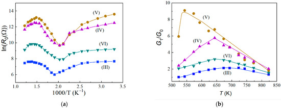
Figure 3.
Temperature dependences of sensors of various compositions: resistance, R0, in pure air (a); and sensor response to 100 ppm H2 (b).
An increase of the resistance (R0) at T > 470 K and its decrease at ≥700 K (Figure 4a) are determined by an increase and subsequent decrease in the density of the negative charge on the surface of the semiconductor. The dependences of the adsorption response on the operating temperature for all the studied films have the form of curves with a maximum at Tmax (Figure 3b and Table 1). With increasing temperature, the response increases when atomic hydrogen interacts with chemisorbed oxygen in the form of , the density of which increases in the temperature range 400–700 K. The decrease in response at T > 540–700 K is due to the predominant desorption of gas from the overheated surface of the sensitive element. As a rule, higher values of Tmax = 720–820 K are observed for films of Compositions (I)–(III). Subsequently, the measurements of the characteristics of sensors were carried out at 670 K, since at this temperature, there is an optimal ratio between the sufficiently high response values and the performance: the response time, tr, does not exceed 30 s.

Figure 4.
Concentration dependences of the response to H2 measured at 670 K for sensors of different compositions: Composition (V) (a); Compositions (IV) and (VI) (b). The inset shows the region G1/G0~exp[eφs].
Figure 4 shows the concentration dependences of the response to hydrogen for the sensors of Compositions (IV)–(VI) measured in the constant heating mode at 670 K. In all cases, exponential segments, G1/G0 ~ exp [n], are observed in the concentration range of 20–1500 ppm of H2 (it is shown in the inset in Figure 4a). In this case, we can assume that the characteristics correspond to a model considering the existence of Schottky barriers at intergrain boundaries [22]. It is possible that H atoms produced due to the dissociative adsorption of H2 can penetrate into the intergrain boundaries and affect the potential barrier height, eφs. Then G1/G0 ~ exp[eφs]. At n > 1500 ppm, a power dependency is realized. A predominant role is played by the over-barrier component of conductivity.
Of particular interest are the data for the films of Composition (V) Pt/Pd/ In2O3 (94.55 at%): Sn (0.5 at%), Dy (4.95 at%) (Figure 4a), whose unique feature is the absence of saturation with an increase in the concentration of H2 up to high values of 25,000 ppm. In this case, G1/G0 reaches 2400–2500. Therefore, for these sensors, there is an unusually high density of hydrogen adsorption centers. For the sensors of Compositions (IV) and (VI) (Figure 4b) at n = 10,000–25,000 ppm, the values of G1/G0 increase insignificantly; that is, the density of the adsorption centers is lower.
Since in case of the studied sensors based on modified indium oxide, the over-barrier component of conductivity is predominant under the action of hydrogen, the above method for determining eϕs can be used. Based on the results of preliminary studies, the following thermal cycling modes were chosen: in the heating cycle, the temperature T1 = 673 K and duration t1 = 8 s; in the cooling cycle, T2 = 473 K and t2 = 6 s. The sensor temperature was increased from T2 up to T1 in about 0.4 s, while it was decreased from T1 down to T2 in about 1 s. In the time dependence of the conductivity, G0, after a step-wise rise of temperature from T2 to T1 at 0.4 < t < 7 s, a decrease of conductivity (Figure 5a) caused by a decrease in the surface density of adsorbed neutral hydroxyl groups (OH-groups) and subsequent increase of Ni due to the adsorption of ions on the vacated sites are observed. At t > 6.82 s, stationary values of Ni(T1), eφs(T1), and G0(T1) are established. At the same time, the condition T2 = 470 K must be satisfied in order for ions to be adsorbed on the SnO2 surface. According to the method of [25], the value of eϕs can be determined by Formula (1):
where k is the Boltzmann’s constant. The conductivity–time profiles (CTP) G0(t) meet the requirements necessary to determine eϕs at the grain boundaries of indium oxide. The shape of the CTP practically does not change under the action of hydrogen (Figure 5b), but the response values at the ends of the cooling cycles, G1/G0(T2), are significantly higher than those in the constant heating mode, G1/G0, and at the ends of the heating cycles, G1/G0(T1).
eϕs = [kT1T2/(T1–T2)] × ln[[G0(T1)/G0(T2)] (T1/T2)0.75] + kT1,
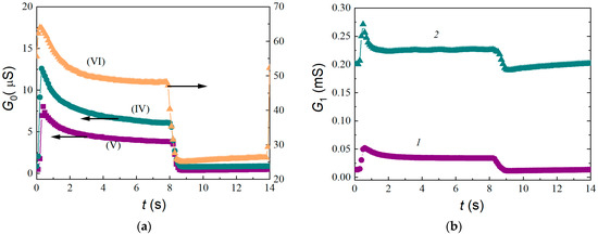
Figure 5.
Conductivity–time profiles in the thermal cycling mode: (a) in pure air for sensors of Compositions (IV)–(VI) and (b) for the sensor of Composition (V) exposed to 100 ppm (Curve 1) and 1000 ppm (Curve 2) of hydrogen.
Table 2 shows the values of eφs and response measured in the constant and pulsed heating modes for samples from all series at fixed hydrogen concentrations. In the case of Samples (I)–(III), there is a high concentration of donor impurity and a reduced density of chemisorbed oxygen. The condition 2d0 << dB is satisfied. Therefore, low values of eφs, i.e., eφs = 0.04–0.06 eV, and response are observed.
Table 2.
Band bending values (eφS) and responses (G1/G0) in the constant heating mode at 670 K and during thermal cycling at the end of the cooling cycle, G1/G0(T2), for H2 concentrations of 1000 and 25,000 ppm.
The decrease in the concentration of tin to 0.5–1 at% and introduction of 4.95 at% dysprosium contribute to the implementation of the condition 2d0 dB, which provides a significant increase in eφs, i.e., eφs = 0.16–0.37 eV, and G1/G0. For these samples, at the end of the cooling cycle, ultrahigh values of the response, G1/G0(T2), are observed at pre-explosive H2 concentrations of 25,000 ppm.
For all sensors known from the literature based on both thin and thick films of tin dioxide commonly used for detecting hydrogen, the signal saturation is observed at n > 3000–5000 ppm, since there is a limited density of H2 adsorption centers on the surface. An analysis of semiconductor hydrogen gas analyzers available on the market shows that, in most cases, they are used to detect low H2 concentrations of 0–2000 ppm. There are no sensors for high hydrogen concentrations. In particular, Figaro (Rolling Meadows, IL, USA), one of the world leaders in this field, produces TGS821 sensors for the range of 30–1000 ppm and TGS600 sensors for the range of 1–30 ppm of H2 [35].
Previously, novel semiconductor sensors with high selectivity and stability were developed [23] for detecting high pre-explosive concentrations of H2 (0.1–2.5 vol%). The sensors were based on thin (~100 nm) nanocrystalline SnO2 films fabricated by the magnetron sputtering of dispersed Pt and Pd layers deposited on the surface, with an addition of 13–14 at% Pt in the bulk. The response values of G1/G0 at 25,000 ppm were 220–230. For the samples of Composition (V) studied in this work based on In2O3 with optimal concentrations of Sn and Dy, the G1/G0 value is an order of magnitude higher and reaches 2400–2500. In the thermal cycling mode, ultrahigh response values are observed at the end of the cooling cycle (Table 2). According to preliminary studies, the sensors are selective for other explosive gases: methane, propane, butane, etc. The response of G1/G0 < 15 to 25,000 ppm of methane is observed. It is important that the sensors can be used to detect both low (50–100 ppm) and high pre-explosive hydrogen concentrations.
4. Conclusions
The defectiveness and electrical and gas-sensitive properties of hydrogen sensors based on thin In2O3 films obtained via the RF magnetron sputtering of specially designed ceramic targets containing various concentrations of indium, tin, and dysprosium oxides were studied. Targets with a diameter of 75 mm and a thickness of 6 mm were obtained by uniaxial static pressing, followed by sintering of powder compacts prepared by the sol–gel method.
The Raman spectra of films with various concentrations of Sn and Dy contain some peaks characteristic of the In2O3 bixbyite syngony. Some of the low-frequency peaks are shifted in frequency, and the maximum of the highest intensity at 130 cm–1 is broadened and observed at 119 cm–1. An important feature of the spectra is the presence of additional maxima at 565, 590, and 648 cm–1. The peaks of low intensity at 565 and 590 cm–1 may be due to the catalysts deposited on the surface in the form of Pd2+ and Pt2+ ions. Dysprosium manifests itself as a bright maximum at 648 cm–1, the intensity of which is higher in samples from Series (III) to (V) with the concentration of (4–4.95) at% of Dy.
Regularities have been established for the changes in properties of films measured under constant heating and thermal cycling modes, depending on the ratio of the concentrations of tin and dysprosium oxides in the targets, as well as on the deposition of dispersed Pt/Pd catalysts on the surface of the films. Sensors containing 10 at% of tin, which creates shallow donor centers in indium dioxide, are characterized by low values of the resistance R0 in pure air, activation energies of temperature dependences of R0, and response G1/G0 to the action of hydrogen. The presence of Pt/Pd on the surface and the introduction of dysprosium into the bulk of the films increase the density of oxygen adsorption centers and the band bending, eφs, at the grain boundaries.
Reducing the concentration of tin to 0.5–1 at% and introducing 4.95 at% of dysprosium contribute to a significant increase in eφs, with eφs = 0.35–0.37 eV, and G1/G0. The presence of the region G1/G0~exp[eφs] in the concentration range n = 20–1500 ppm of H2 indicates the predominant role of the over-barrier component of conductivity. An important feature of sensors based on Pt/Pd/In2O3 (94.55 at%): Sn (0.5 at%), Dy (4.95 at%) is the absence of signal saturation when n increases to high values of 25,000 ppm of H2. In this case, G1/G0 reaches 2400–2500.
The mechanism of the dysprosium effect is determined by the higher energy of breaking the bond with oxygen Dy–O compared to In–O and Sn–O bonds. During technological annealing under the film crystallization, impurity atoms segregate on the surface of microcrystals and actively form strong bonds with lattice oxygen, contributing to the formation of superstoichiometric indium and, possibly, tin, which, together with Dy3+ ions, sharply increases the density of oxygen and hydrogen adsorption centers. On the basis of original films obtained by the RF magnetron sputtering of oxide targets with an optimal ratio of Sn and Dy impurity concentrations, unique sensors for detecting hydrogen in a wide range of concentrations, including pre-explosive values of 25,000 ppm, can be created.
Based on the results obtained, we plan to further optimize the composition and methods of obtaining films to increase the efficiency of sensors based on In2O3, detailed studies of their composition, structure and physicochemical properties, as well as the study of selectivity and testing of the service life.
Author Contributions
Conceptualization, N.M., T.M. and V.S.; methodology, V.Z. and E.C.; validation, N.M., T.M. and V.S.; formal analysis, N.M., T.M. and N.S.; investigation, V.S., N.S., V.Z., E.C. and I.L.; resources, N.M., T.M. and V.S.; writing—original draft preparation, N.M. and T.M.; visualization, V.S., N.S. and I.L.; supervision, N.M., T.M. and V.S.; project administration, N.M. and T.M.; funding acquisition, N.M. All authors have read and agreed to the published version of the manuscript.
Funding
This study was supported by the Tomsk State University Development Programme (Priority-2030).
Institutional Review Board Statement
Not applicable.
Informed Consent Statement
Not applicable.
Data Availability Statement
The data presented in this study are available upon request from the corresponding author.
Acknowledgments
The Raman spectroscopy research was carried out with the equipment of Tomsk Regional Core Shared Research Facilities Center of National Research Tomsk State University. The Center was supported by the Ministry of Science and Higher Education of the Russian Federation, grant no. 075-15-2021-693 (no. 13.RFC.21.0012).
Conflicts of Interest
The authors declare no conflict of interest.
References
- Sezemsky, P.; Burnat, D.; Kratochvil, J.; Wulff, H.; Kruth, A.; Lechowicz, K.; Janik, M.; Bogdanowicz, R.; Cada, M.; Hubicka, Z.; et al. Tailoring properties of indium tin oxide thin films for their work in both electrochemical and optical label-free sensing systems. Sens. Actuators B Chem. 2021, 343, 130173. [Google Scholar] [CrossRef]
- Frank, G.; Köstlin, H. Electrical properties and defect model of tin-doped indium oxide layer. Appl. Phys. A 1982, 27, 197–206. [Google Scholar] [CrossRef]
- Ray, S.; Banerjee, R.; Basu, N.; Batabyal, A.K.; Barua, A.K. Properties of tin doped indium oxide thin films prepared by magnetron sputtering. J. Appl. Phys. 1983, 54, 3497–3501. [Google Scholar] [CrossRef]
- Stadler, A. Transparent Conducting Oxides—An Up-To-Date Overview. Materials 2012, 5, 661–683. [Google Scholar] [CrossRef]
- Txintxurreta, J.; G-Berasategui, E.; Ortiz, R.; Hernández, O.; Mendizábal, L.; Barriga, J. Indium Tin Oxide Thin Film Deposi-tion by Magnetron Sputtering at Room Temperature for the Manufacturing of Efficient Transparent Heaters. Coatings 2021, 11, 92. [Google Scholar] [CrossRef]
- Zhang, M.; Xu, W.; Shen, H.; Wang, J.; Han, J. New research progress of transparent conductive oxide films. Yadian Yu Shengguang Piezoelectrics Acoustooptics 2010, 32, 811–815. [Google Scholar]
- Hosono, H.; Ueda, K. Transparent Conductive Oxides. In Book Springer Handbook of Electronic and Photonic Materials, 2nd ed.; Kasap, S., Capper, P., Eds.; Springer Nature: Cham, Switzerland, 2017; pp. 1391–1404. [Google Scholar] [CrossRef]
- Mokrushin, A.S.; Fisenko, N.A.; Gorobtsov, P.Y.; Simonenko, T.L.; Glumov, O.V. Pen plotter printing of ITO thin film as a highly CO sensitive component of a resistive gas sensor. Talanta 2021, 221, 121455. [Google Scholar] [CrossRef]
- Korotcenkov, G.; Cho, B.K. The role of grain size on the thermal instability of nanostructured metal oxides used in gas sensor applications and approaches for grain-size stabilization. Prog. Cryst. Growth 2012, 58, 167–208. [Google Scholar] [CrossRef]
- Zhao, Y.; Wang, S.; Fan, S.; Hua, Z.; Wu, Y.; Tian, X.; Yuan, W. Selective detection of methane by Pd-In2O3 sensors with a catalyst filter film. Sens. Actuators B Chem. 2021, 328, 129030. [Google Scholar] [CrossRef]
- Korotcenkov, G.; Boris, I.; Brinzari, V.; Han, S.H.; Cho, B.K.; Lychkovsky, Y.N. In2O3: Ga and In2O3: P-based one-electrode gas sensors: Comparative study. Ceram. Int. 2015, 41, 7478–7488. [Google Scholar] [CrossRef]
- Ullah, H.; Yamani, Z.H.; Qurashi, A.; Iqbal, J.; Safeen, K. Study of the optical and gas sensing properties of In2O3 nanoparticles synthesized by rapid sonochemical method. J. Mater. Sci. Mater. Electron. 2020, 31, 17474–17481. [Google Scholar] [CrossRef]
- Rahamim, G.; Mirilashvili, M.; Nanikashvili, P.; Greenberg, E.; Shpaisman, H.; Grinstein, D.; Welner, S.; Zitoun, D. Hydrogen sensors with high humidity tolerance based on indium-tin oxide colloids. Sens. Actuators B Chem. 2020, 310, 127845. [Google Scholar] [CrossRef]
- Anand, K.; Thangaraj, R.; Kohli, N.; Singh, R.C. Structural, Optical and Ethanol Gas Sensing Properties of In2O3 and Dy3+: In2O3 Nanoparticles. AIP Conf. Proc. 2014, 1591, 477–480. [Google Scholar] [CrossRef]
- Carreno, N.L.V.; Maciel, A.P.; Leite, E.R.; Lisboa-Filho, P.N.; Longo, E.; Valentino, A.; Probst, L.E.D.; Paiva-Santos, C.O.; Schreiner, W.H. The influence of cation segregation on the methanol decomposition on nanostructured SnO2. Sens. Actuators B Chem. 2002, 86, 185–192. [Google Scholar] [CrossRef]
- Korotcenkov, G.; Cho, B.K. Metal oxide composites in conductometric gas sensors: Achievements and challenges. Sens. Actuators B Chem. 2017, 244, 182–210. [Google Scholar] [CrossRef]
- Leite, R.; Maciel, A.P.; Weber, I.T.; Lisboa-Filho, P.N.; Longo, E.; Paiva-Santos, C.O.; Andrade, A.V.C.; Pakoscimas, C.A.; Maniette, Y.; Schreiner, W.H. Development of metal oxide nanoparticles with high stability against particle growth using a metas solid solution. Adv. Mater. 2002, 14, 905–908. [Google Scholar] [CrossRef]
- Cheng, L.; Ma, S.Y.; Li, X.B.; Luo, J.; Li, W.Q.; Li, F.M.; Mao, Y.Z.; Wang, T.T.; Li, Y.F. Highly sensitive acetone sensors based on Y-doped SnO2 prismatic hollow nanofibers synthesized by electrospinning. Sens. Actuators B Chem. 2014, 200, 181–190. [Google Scholar] [CrossRef]
- Cheng, L.; Ma, S.Y.; Wang, T.T.; Luo, J.; Li, X.B.; Li, W.Q.; Mao, Y.Z.; Gz, D.J. Highly sensitive acetic acid gas sensor based on coral-like and Y-doped SnO2 nanoparticles prepared by electrospinning. Mater. Lett. 2014, 137, 265–268. [Google Scholar] [CrossRef]
- Kazuyoshi, I.; Koki, Y.; Masashi, K. Sputtering Target, Semiconductor Film and Semiconductor. Device. Patent US8333913B2, 18 December 2012. [Google Scholar]
- Maksimova, N.K.; Almaev, A.V.; Sevastyanov, E.Y.; Potekaev, A.I.; Chernikov, E.V.; Sergeychenko, N.V.; Korusenko, P.M.; Nesov, S.N. Effect of Additives Ag and Rare-Earth Elements Y and Sc on the Properties of Hydrogen Sensors Based on Thin SnO2 Films during Long-Term Testing. Coatings 2019, 9, 423. [Google Scholar] [CrossRef]
- Sevastyanov, E.Y.; Maksimova, N.K.; Novikov, V.A.; Rudov, F.V.; Sergeychenko, N.V.; Chernikov, E.V. Effect of Pt, Pd, Au additives on the surface and in the bulk of tin dioxide thin films on the electrical and gas-sensitive properties. Semiconductors 2012, 46, 801–809. [Google Scholar] [CrossRef]
- Maksimova, N.K.; Sevastyanov, E.Y.; Chernikov, E.V.; Korusenko, P.M.; Nesov, S.N.; Kim, S.V.; Biryukov, A.A.; Sergeychenko, N.V.; Davletkildeev, N.A.; Sokolov, D.V. Sensors based on tin dioxide thin films for the detection of pre-explosive hydrogen concentrations. Sens. Actuators B Chem. 2021, 341, 130020. [Google Scholar] [CrossRef]
- Maksimova, N.K.; Khludkova, L.S.; Biryukov, A.A.; Sevast’yanov, E.Y.; Chernikov, E.V.; Kushnarev, B.O. The Stability of Liquid Hydrocarbon Vapor Sensors Based on SnO2 Thin Films Modified with Various Catalysts. Tech. Phys. 2021, 66, 999–1008. [Google Scholar] [CrossRef]
- Gaman, V.I.; Sevast’yanov, E.Y.; Maksimova, N.K.; Almaev, A.V.; Sergeichenko, N.V. Characteristics of the semiconductor resistive hydrogen sensors in the thermo-cyclic operation mode. Russ. Phys. J. 2014, 56, 1427–1434. [Google Scholar] [CrossRef]
- Malinovskaya, T.; Ghyngazov, S.; Zhek, V. Thermal destruction of coprecipitated hydroxides of indium and dysprosium. J. Therm. Anal. Calorim. 2019, 138, 1871–1877. [Google Scholar] [CrossRef]
- Wang, C.Y.; Dai, Y.; Pezoldt, J.; Lu, B.; Kups, T.; Cimalla, V.; Ambacher, O. Phase stabilization and phonon properties of single crystalline rhombohedral indium oxide. Cryst. Growth Des. 2008, 8, 1257–1260. [Google Scholar] [CrossRef]
- Kranert, C.; Schmidt-Grund, R.; Grundmann, M. Raman active phonon modes of cubic In2O3. Phys. Status Solidi RRL 2014, 8, 554–559. [Google Scholar] [CrossRef]
- Gan, J.; Lu, X.; Wu, J.; Xie, S.; Zhai, T.; Yu, M.; Zhang, Z.; Mao, Y.; Wang, S.C.I.; Shen, Y.; et al. Oxygen vacancies promoting photochemical performance of In2O3 nanocubes. Sci. Rep. 2013, 3, 1021. [Google Scholar] [CrossRef]
- Berengue, O.M.; Rodrigues, A.D.; Dalmaschio, C.J.; Lanfredi, A.J.C.; Leite, E.R.; Chiquito, A.J. Structural characterization of indium oxide nanostructures: A Raman analysis. J. Phys. D 2010, 43, 045401. [Google Scholar] [CrossRef]
- Lee, H.; Kim, B.; Gao, C.Y.; Choi, H.J.; Ko, J.H.; Seo, C.H.; Park, J. Raman spectroscopy study of solution processed In2O3 thin films: Effect of annealing temperature on the characteristics of In2O3 semiconductors and thin-film transistors. Mol. Cryst. Liq. Cryst. 2019, 679, 38–47. [Google Scholar] [CrossRef]
- Yadav, K.; Mehta, B.R.; Singh, J.P. Synthesis and Raman spectrum of crystalline indium oxide micro-rods with rectangular cross-section. Solid State Phys. AIP Conf. Proc. 2014, 1591, 409–410. [Google Scholar] [CrossRef]
- Rumyantseva, M.N.; Gaskov, A.M.; Rosman, N.; Pagnier, T.; Morante, J.R. Raman Surface Vibration Modes in Nanocrystalline SnO2: Correlation with Gas Sensor Performances Interfaces. Chem. Mater. 2005, 17, 893–901. [Google Scholar] [CrossRef]
- Luo, Y.R. Comprehensive Handbook of Chemical Bond Energies, 1st ed.; CRC Press: Boca Raton, FL, USA, 2007; Volume 1655. [Google Scholar] [CrossRef]
- FIGARO USA, Inc. Gas Sensors & Modules. Available online: https://www.figarosensor.com/product/sensor/ (accessed on 10 November 2022).
Disclaimer/Publisher’s Note: The statements, opinions and data contained in all publications are solely those of the individual author(s) and contributor(s) and not of MDPI and/or the editor(s). MDPI and/or the editor(s) disclaim responsibility for any injury to people or property resulting from any ideas, methods, instructions or products referred to in the content. |
© 2022 by the authors. Licensee MDPI, Basel, Switzerland. This article is an open access article distributed under the terms and conditions of the Creative Commons Attribution (CC BY) license (https://creativecommons.org/licenses/by/4.0/).