Article

Electrostatic Spray Deposition of Al-Doped ZnO Thin Films for Acetone Gas Detection

1
Department of Creative Convergence Engineering, Hanbat National University, Yuseong-ku, Daejeon 305-719, Republic of Korea
2
Research Institute of Printed Electronics & 3D Printing, Hanbat National University, Yuseong-ku, Daejeon 305-719, Republic of Korea
*
Author to whom correspondence should be addressed.
Processes 2023, 11(12), 3390; https://doi.org/10.3390/pr11123390
Submission received: 8 November 2023 / Revised: 4 December 2023 / Accepted: 5 December 2023 / Published: 8 December 2023

Abstract

:
In this study, pure ZnO and Al-doped ZnO(AZO) thin films were coated onto a SiO2 wafer using the electrostatic spray deposition (ESD) process for acetone gas detection under laboratory conditions. Voltage levels were varied to determine the optimal conditions for producing thin films with the highest uniformity. The results indicate that the optimal coating voltage for achieving the highest uniformity of the coated films is 2.9 kV for ZnO and 2.6 kV for AZO. The thin films were produced under these optimal ESD conditions by adjusting the coating time, and gas sensors were fabricated by printing electrodes using a reverse offset process on top of the thin films. Analysis of the sensing response revealed that the AZO-coated gas sensor with a 200 s deposition exhibited the best acetone-sensing ability at 300 °C, with a maximum response of 13.41 at 10 ppm. Furthermore, the fabricated gas sensors effectively detected acetone gas even at a low concentration of 2 ppm, demonstrating high selectivity in comparison to other gases.

1. Introduction

In recent years, the release of volatile organic compounds (VOCs) has increased with rapid industrialization. Acetone is a well-known colorless VOC with a strong odor and widely used in laboratories, factories, and pharmaceutical manufacturing plants [1,2]. Additionally, it is a key solvent in the production of methacrylate, which is used in plastic manufacturing [3]. The inhalation of acetone can lead to headaches, allergies, and anesthesia, as it is toxic to the nervous system. Exposure to high concentrations of acetone (>173 ppm) can anesthetize the central nervous system, causing damage to important organs in the human body [4,5]. Consequently, major safety institutions such as the National Institute of Occupational Safety and Health (NIOSH) and the European Agency for Safety and Health at Work (EU-OSHA) restrict the level of human exposure to acetone in indoor and work environments [6]. In the regulation of acetone exposure, NIOSH specifies a time-weighted average (TWA) limit of 250 ppm on its official website https://www.cdc.gov/niosh/npg/npgd0004.html (accessed on 27 November 2023). Meanwhile, EU-OSHA has established an 8 h time-weighted average limit of 500 ppm, as specified on its official website https://eur-lex.europa.eu/legal-content/EN/TXT/?uri=CELEX%3A02000L0039202105-20 (accessed on 27 November 2023). These limits are established to restrict acetone exposure in occupational settings, aiming to minimize health impacts and maintain a safe working environment. Therefore, the acetone gas sensors used in indoor and workplace environments should exhibit sufficiently high sensitivity to detect ppm-level concentrations of acetone with exceptional selectivity for acetone.
Metal oxide semiconductors (MOSs) are commonly applied as detectors in gas sensors due to their low cost, rapid response, and excellent detection characteristics [7]. Several studies have investigated sensors for detecting acetone gas using materials such as SnO2, Fe2O3, WO3, and ZnO [8,9,10,11]. Among these, ZnO is an N-type semiconductor easily manufactured and allows mass production with good responses to gases. Consequently, different methods have been explored to enhance the gas detection ability of ZnO [12]. Doping is an effective way to improve the sensitivity response of the gas sensor. Yoo et al. explored various materials for doping ZnO, including Cu, Co, and Al, and investigated the sensing responses of these materials to various concentrations of acetone. Among the studied materials, Al-doped ZnO exhibits the highest sensitivity to acetone gas [13].
Traditionally, ZnO thin films have been produced through sputtering or thermal deposition for use as detection layers in sensors [14,15]. However, these processes require high temperatures or vacuum conditions, adding complexity and expense to the production process. To overcome these drawbacks, various research centers and corporations have been investigating electrode printing [16]. Electrode printing utilizes general printing techniques, conductive materials, semiconductors, and dielectric materials to create electronic products. Devices fabricated using this technology are thin and lightweight. This environmentally friendly process offers cost advantages over traditional semiconductor methods and allows for large-scale production offering the advantage of low cost. In contrast, the conventional semiconductor process requires costly devices and involves multiple steps including deposition, washing, masking, and etching to form a patterned layer. The electrode-printing process requires fewer steps and allows for continuous processing, including lamination, with the possibility of micro-patterning and thin film coating [17,18]. Electrode-printing methods include gravure offset, reverse offset, and screen printing as contact processes, as well as inkjet, slot-die, and electrostatic spray deposition (ESD) as non-contact processes [19,20,21,22,23,24].
The ESD process is initiated by applying a voltage across the nozzle of the system. The resulting electrostatic force between the capillary tube and the substrate leads to the spraying of the solution at the tip of the capillary tube. Although this process has primarily been used in the painting and coating industries in the past, its scope of application has recently expanded to include the production of transparent electrodes, organic solar cells, and gas sensors. ESD has also been utilized in the production of gas sensors, such as for fabricating ZnO thin films for NO2 gas sensors or H2S gas sensors with WO3 as the detection layer [25,26]. Utilizing an acetone gas sensor enables the diagnosis of medical conditions through respiratory analysis. The acetone concentration in the breath of a healthy individual typically ranges from 0.2 to 1.8 ppm. In contrast, diabetic patients exhibit higher acetone concentrations in their breath, ranging from 1.25 to 2.5 ppm. Therefore, employing an acetone gas sensor allows for the early detection of diabetes by confirming elevated acetone levels in the patient’s breath [13].
In this study, we have developed a fabrication process of the gas sensor using the printing process. The electrostatic spray deposition (ESD) process is employed to deposit ZnO and Al-doped ZnO (AZO) thin films onto the SiO2 wafer by varying the voltage level, and the film thickness is analyzed to identify the conditions for fabricating thin films with the highest uniformity. By printing an Ag electrode on the coated films using the reverse offset process, acetone gas sensors were created. The gas response of the ZnO and AZO thin films were investigated in the range of 250–400 °C. Different gas response properties, such as sensitivity, selectivity and response and recovery time, were measured. Analysis of the sensing response of the fabricated ZnO and AZO gas sensors revealed that AZO showed a better performance than ZnO thin film, and compared to other (NH3 and CO) gases, the selectivity of the AZO sensor showed the highest response towards acetone gas.
Hence, our present study deals with the detailed fabrication process of fully printed gas sensors. By printing electrodes on films produced through the ESD process, we demonstrate the applicability of gas sensors fabricated through the ESD process.

2. Materials and Methods

2.1. Materials and Characterization

ZnO nanoparticle ink (Sigma Aldrich Co., St. Louis, MO, USA) and Al-doped ZnO (AZO) (Sigma Aldrich Co., St. Louis, MO, USA) nanoparticle ink were used as the sensing layer. ZnO nanoparticle ink and AZO nanoparticle ink were purchased from Sigma Aldrich Co., St. Louis, MO, USA and used without any further modification. A 2.5 wt% solution of ZnO nanoparticle ink was prepared in ethylene glycol, and a 2.5 wt% solution of AZO nanoparticle ink containing 3.15 mol% Al-doped ZnO was also dispersed in ethylene glycol. The viscosity of the ink ranged from 8 to 14 cP for both ZnO and AZO.
The characteristics of ZnO and AZO were analyzed using X-ray diffractometry (XRD), scanning electron microscopy (SEM) and X-ray photoelectron spectroscopy (XPS). The structural properties of ZnO and AZO were examined using XRD (D8-Discover (Bruker AXS, Karlsruhe, Germany) using monochromatic Cu-Kα radiation (λ = 1.5406 Å). The film thicknesses were determined using FE-SEM (S-4800), and XPS (Thermo Fisher Scientific, Waltham, MA, USA) was used to understand the surface chemical properties.

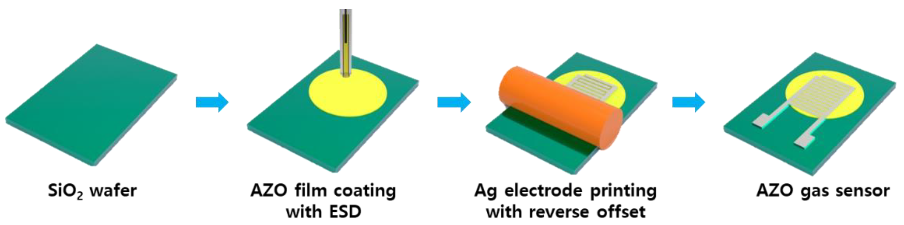
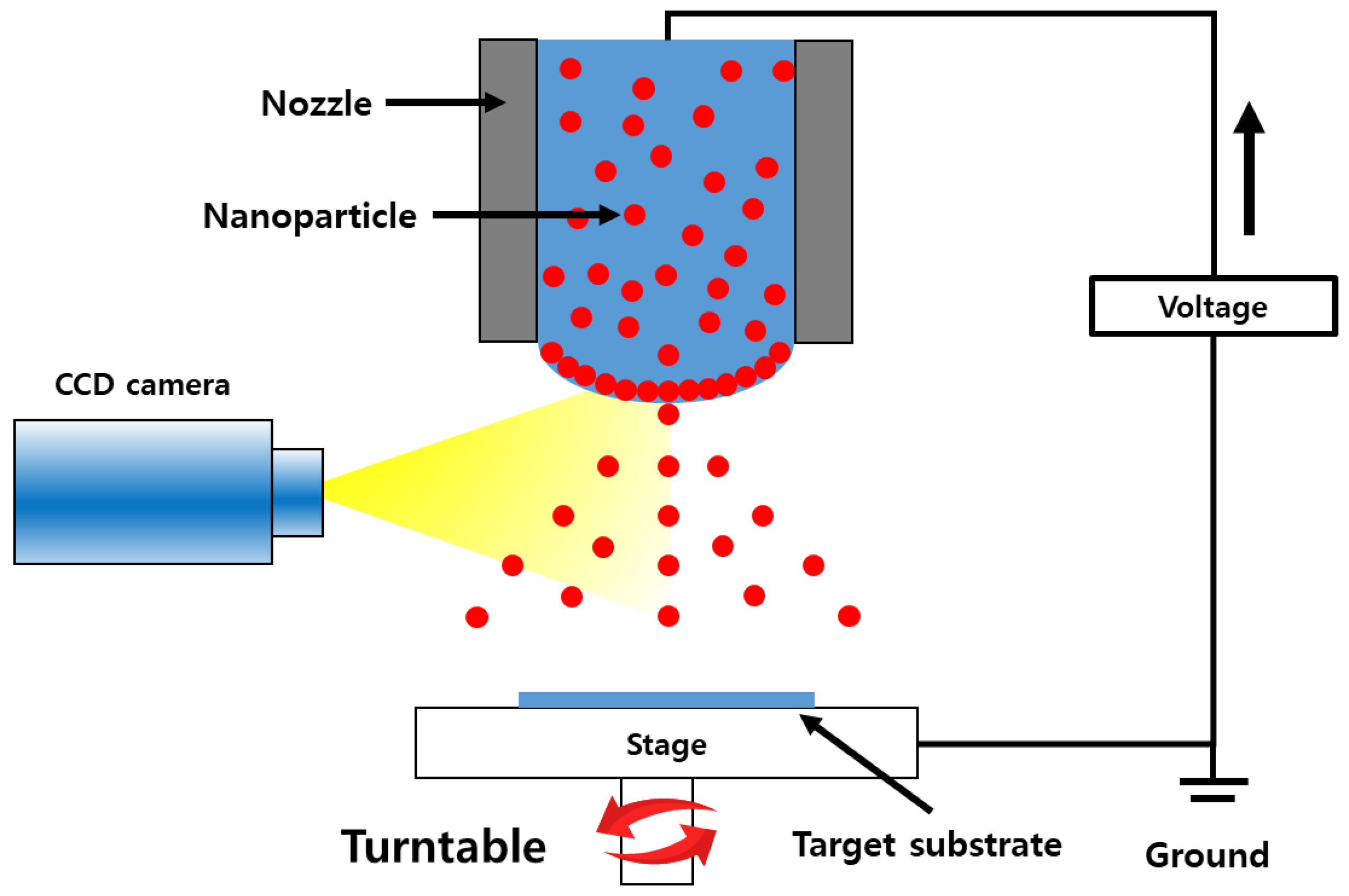
2.2. Sensing Layer Coating

ZnO and Al-doped ZnO (AZO) gas sensors were fabricated by following the series of steps out-lined in Figure 1 Initially, the SiO2 wafer substrates were cleaned using acetone and isopropyl alcohol (IPA). ZnO and AZO nanoparticle inks were deployed onto the SiO2 wafers to produce ZnO and AZO thin films through an electrostatic spray deposition (ESD) process. The viscosity of both inks ranged between 8 and 14 cp. The principles of the ESD process are illustrated in Figure 2. In this technique, the solution is injected into the capillary tube or spray nozzle. For uniform coating, the substrate being coated rotates consistently at 6 rpm. By applying a voltage to the nozzle, an electrostatic force between the capillary tube and the substrate occurs, which causes the solution to be sprayed uniformly from the tip of the capillary tube. An advantage of ESD under atmospheric conditions is that it does not require a vacuum device, thus reducing the costs and ensuring high reproducibility [24]. Additionally, the sprayed droplets tend to be deposited primarily at the peak of the structure and a porous structure can be formed which enhances gas detection [26]. The inner diameter and length of the nozzle were 61 μm and 75 mm, respectively, with a distance of 20 mm between the nozzle and the substrate. The stage was rotated at 0.1 rpm during spraying to achieve thin films with maximum uniformity. After repeated cycles of 10 s of spraying followed by 2 min of drying at 150 °C, the film-coating process was completed. The resulting coated thin films were annealed at 600 °C for 1 h. The spray times were varied for 50, 100, 150, and 200 s. The same set of steps was applied to fabricate sensors for both ZnO or AZO detection layers, and the performance of the sensors was comparatively analyzed.

2.3. Electrode Printing with Reverse Offset

To print an interdigitated electrode (IDE) structure on the coated thin films, a reverse offset process was performed with Ag ink (ANP Co., Ltd., Sejong, Republic of Korea). In reverse offset printing, Ag ink is applied through spin coating and then transferred to the substrate using a double-layer blanket (DLB) roll to create an electrode in an Reverse offset process. In this study, spin coating was performed at 3000 rpm for 20 s, and the electrode offset conditions in the reverse offset printing were identical to those in a previous study [20]. The IDE consisted of 50 digits with a line width of 30 μm and an electrode spacing of 130 μm, resulting in an IDE size of 8 mm × 6 mm. The printed electrode was dried at 150 °C for 25 min and subsequently annealed at 450 °C for 25 min. The scanning electron microscope (SEM) image in Figure 3 confirms that the printed pattern closely matched the values set at the cliché.

2.4. Gas Sensing Measurement

For the fabricated gas sensors, measurements were carried out using a mass flow controller (MFC, PHOCOS, Seoul, Republic of Korea) as shown in Figure 4. The gas detection characteristics were assessed using the MFC and a gas detection system comprising a Keithley 2400 source measure unit (SMU). Two probes were connected to the electrodes of the sensor, and the sensor operating voltage was fixed at 1 V. Sensor data acquisition was performed using custom software developed by PHOCOS (Seoul, Republic of Korea), and the data were collected using a computer connected to the interface (serial port: S/N ML 70610007). Sensor data were then filtered, receiving and processing 10 data points per second.
The total flow in the chamber was 250 sccm, and the concentration of acetone gas was maintained at 2–10 ppm by regulating the flow of air and acetone gas. The gas sensor temperature was set in the range of 250–400 °C. Equation (1) defines the gas sensor response, where Ra and Rg represent the resistance in dry air and acetone gas, respectively.
Sensor response = Ra/Rg

3. Results and Discussion

3.1. XRD Crystal Structure Analysis

Figure 5 represents the XRD patterns of ZnO and AZO. The XRD patterns of ZnO and AZO match well with JCPDS: #36-1451 and exhibit hexagonal wurtzite structure. Three strong peaks corresponding to (100), (002), and (101) were observed in both ZnO and AZO nanoparticles (NPs). No other impurity peaks were observed, confirming that the hexagonal structure of ZnO remained unaltered despite Al3+ doping [27,28,29].
The crystallite sizes (D) of ZnO and AZO were calculated using Scherrer’s formula (Equation (2)), where β represents the full width at half maximum (FWHM) of a peak, and λ is the wavelength of incident X-rays [30]. The ZnO particle size is 10.57 nm, and AZO particle size is 25.44 nm.
D = 0.9 λ β c o s θ
To assess the impact of Al doping, an analysis of the (101) peak in the XRD graph was conducted. The results revealed that the peak for pure ZnO was at 36.32°, while for AZO, it shifted to 36.34°, indicating a 0.02° shift due to Al doping. This shift of the (101) peak position by 0.02° is attributed to the smaller atomic radius of the doped Al3+ (0.53 Å) ion, as opposed to the atomic radius of Zn2+ (0.74 Å) [13].

3.2. Analysis of Thin Films Formed by the ESD Process

Figure 6 illustrates the spray pattern observed at each applied voltage when the thin films were coated onto the substrate using ZnO and AZO nanoparticle inks via the ESD process. The applied voltage was incrementally increased by 0.3 kV starting at 2.9 kV for ZnO and 2.6 kV for AZO with measurements taken at consistent intervals. With the use of ZnO ink, both the ink quantity and spray angle increased and the dispersed ink was concentrated at the center as the electrostatic force applied to the ink increased with the rising voltage. In the case of the AZO ink, an increase in the applied voltage led to a greater quantity of dispersed ink, resulting in an expanded spray angle. Therefore, the minimum voltage was required for coating to achieve the maximum uniformity of the thin films. Subsequently, the thickness of the center and the right and left sides of the coated films were analyzed. Images for the film thickness analysis were acquired using an S-4800FE-SEM device (HITACHI, Tokyo, Japan). Figure 7 displays the images used to analyze the thickness variation in the thin films coated onto the substrate using ZnO at 2.9 kV and 3.8 kV. For coating times of 100 s, Figure 8 presents the images used for the analysis of the thickness variation in the thin films coated onto the substrate using AZO at 2.6 kV and 3.5 kV. As is evident in these figures, raising the applied voltage increased the amount of ink dispersed at the center of the film, leading to increased thickness variation. Additional images for the thickness variation analysis with variation in the applied voltage are presented in Figures S1 and S2.
Analysis of the thicknesses of the ZnO and AZO thin films coated onto the substrate for 100 s at each applied voltage revealed that the highest level of uniformity was achieved at the minimum applied voltage of 2.9 kV for ZnO and 2.6 kV for AZO. Based on these findings, the final voltage for the coating process was set at 2.9 kV for ZnO and 2.6 kV for AZO.
Figure 9 displays the images used to analyze the thicknesses of the thin films coated onto the substrate at the minimum applied voltage (2.9 kV for ZnO and 2.6 kV for AZO) based on the total coating time. As shown, the thicknesses were uniform across the fabricated thin films, regardless of the total coating time. According to the figure, despite the lower applied voltage for AZO compared to ZnO, the thickness of the film was greater. This is attributed to the enhanced conductivity of AZO ink due to the aluminum doping, which facilitates the ejection of a larger volume of ink even at lower applied voltages.

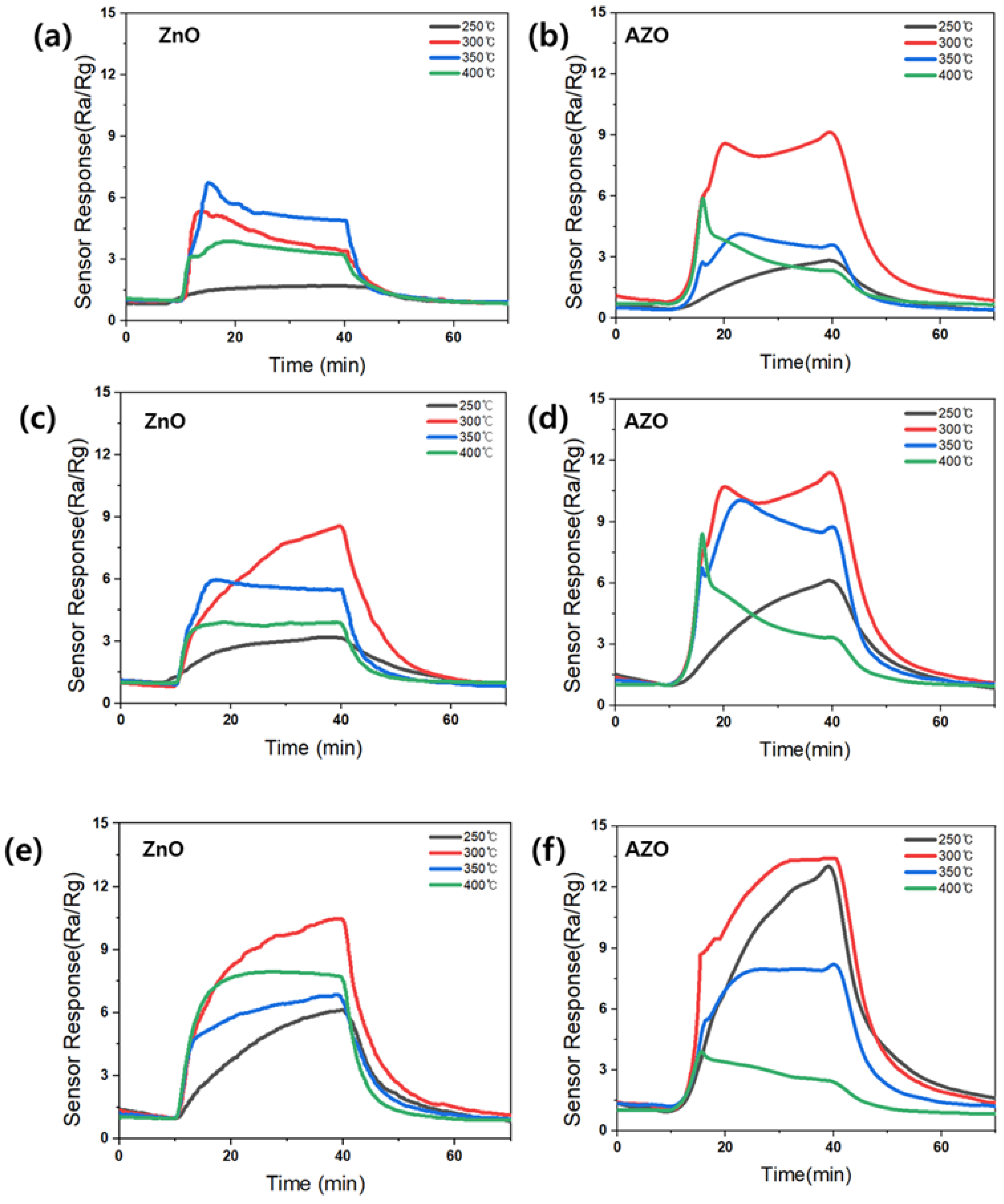
3.3. The Effect of Coating Time on the Sensing Response

Figure 10 shows the response to acetone for the fabricated gas sensors employing the ZnO and AZO films deposited with different coating times. The sensors employing the films deposited by coating for 100, 150, and 200 s are denoted as ZnO (AZO)_100, 150, and 200, respectively. The measurements at 50 s indicated no sensing response and were thus excluded. Each sensor was exposed to 10 ppm acetone gas at varying temperatures, and the sensing responses were analyzed. Figure 11 provides a summary of the maximum responses recorded for the fabricated sensors. Both ZnO and AZO sensors coated for 200 s exhibited the strongest response at 300 °C. The response of the fabricated sensors increased as the detection temperature increased to 300 °C. However, beyond a certain optimal temperature level, a decrease in the response was observed, possibly due to the desorption of oxygen adsorbed onto the surface of ZnO [31]. The ZnO/AZO thin films coated for 200 s consist of nanoparticles, as depicted in Figure 8, and their performance in detecting acetone gas is enhanced by increasing the film thickness. Nonetheless, a significant difference in the sensing response of the ZnO and AZO gas sensors was noted. When exposed to 10 ppm acetone gas at the same temperature, the AZO sensor exhibited a stronger response than the ZnO sensor. This enhancement in the gas detection characteristics of ZnO is likely attributed to the contribution of Al doping.

3.4. Surface Defects and the Analysis of Mechanisms

To analyze the surface chemical properties of the coated ZnO and AZO thin films, XPS analysis was performed. The results are presented in Figure 12. Figure S3 shows the survey scan spectra for ZnO and AZO. In Figure S3, the Al peak at a binding energy of 74.7 eV corresponds to the Al 2p peak, indicating the successful inclusion of Al atoms by substituting Zn2+ into ZnO [32]. The peaks at 1044.94 eV and 1021.84 eV in the Zn spectrum (Figure 12a) correspond to the Zn 2p1/2 and Zn 2p3/2 states of Zn2+, respectively. Additionally, the difference in the binding energy of the two peaks in the Zn 2p spectrum for ZnO and AZO is 23.1 eV, indicating a 2+ oxidation state of Zn [33]. The binding energy of the ZnO samples with Al doping (Figure 12b) is slightly higher than that of the pure ZnO samples. An increase in the binding energy reflects electronic interactions between ZnO and the dopant, which accounts for the improved gas-sensing response of ZnO with Al doping [34]. Figure 12c,d represent the O1s spectra of ZnO and AZO, respectively. The weak peaks at 530.3 eV for ZnO and at 530.8 eV for AZO correspond to the O2− ion in the Zn-O bond [35,36]. The strong peak at 532.1 eV corresponds to oxygen vacancy, indicating a hypoxic state caused by the loss of surface oxygen. Compared to the XPS profile of ZnO, that of AZO (Figure 12d) displayed a peak at a higher binding energy of 532.6 eV. This implies that as a result of the oxygen vacancies in AZO, the sensing response increased compared to that of pure ZnO [37].
Figure 13 represents a schematic diagram of the sensing mechanism of the acetone gas sensors, which primarily follows the behavior of N-type semiconductors. As the temperature of ZnO increases, the transition of electrons occurs from the valence band to the conduction band [13]. These conduction band electrons then react with the atmospheric oxygen on the surface, leading to adsorption. Adsorption of atmospheric oxygen creates a depletion region, resulting in an increase in the resistance [3]. When a reducing gas like acetone enters into this region, it reacts with the adsorbed oxygen on the ZnO surface and induces a response as described in Equation (3), thus releasing the adsorbed electrons. Consequently, the resistance of the gas sensor exposed to the gas decreases. In the case of AZO, the higher electronegativity of the Al3+ dopant compared to that of Zn2+ leads to more adsorption than in pure ZnO, enhancing the sensing response.
CH3COCH3 (gas) + 8O(ads) → 3CO2 + 3H2O + 8e

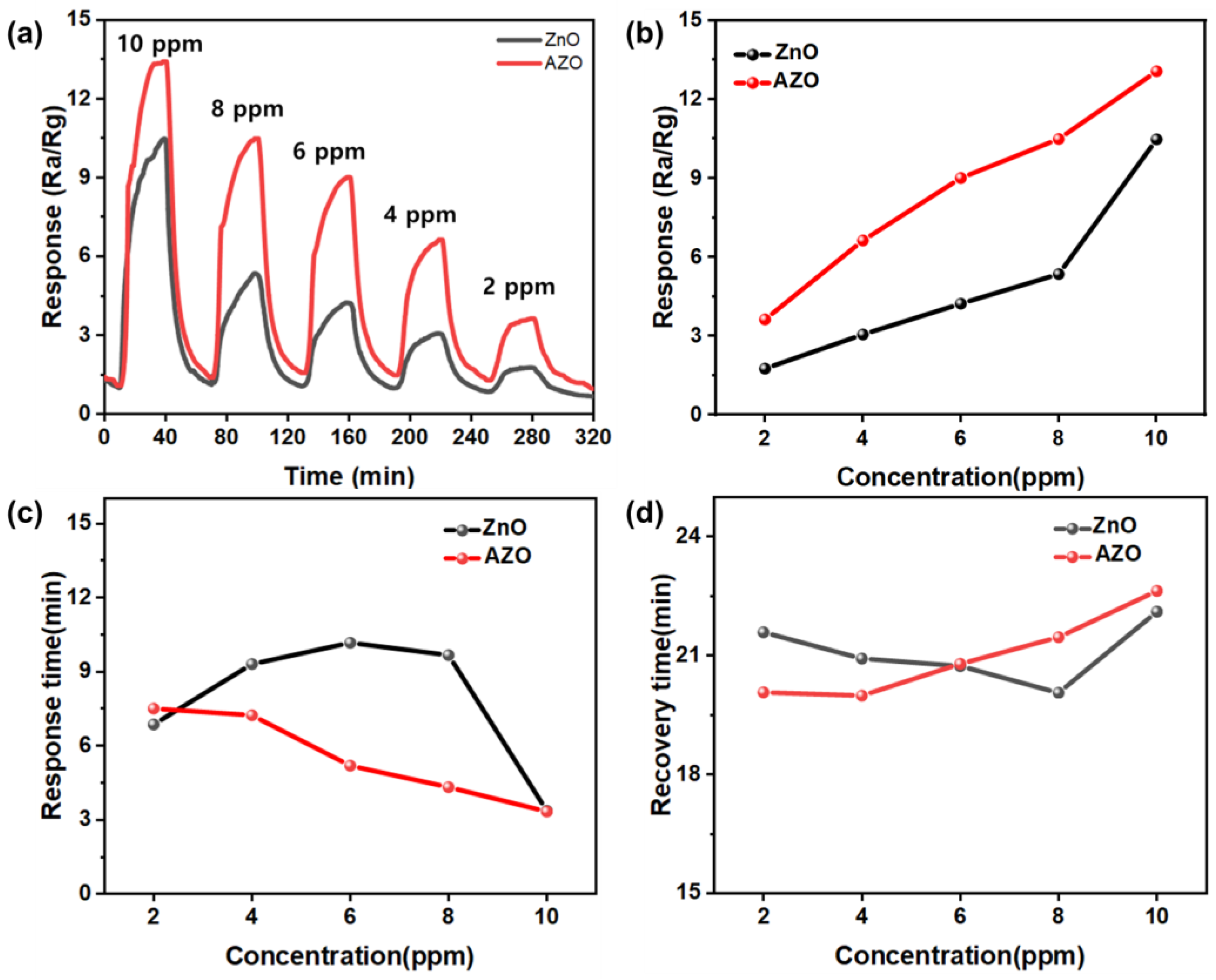
3.5. The Sensitivity and Selectivity of Sensors

The response of each sensor was analyzed under the optimal conditions (temperature: 300 °C; thickness: 200 nm) with varying acetone gas concentrations, as shown in Figure 14a. The responses were measured at different acetone gas concentrations of 2, 4, 6, 8, and 10 ppm. Figure 14b shows the maximum responses of ZnO and Al-doped ZnO NPs to acetone gas, indicating that the response decreased as the gas concentration decreased for both the ZnO and AZO sensors. A concentration-dependent variation in the response to acetone gas was observed for both sensors. The AZO sensor exhibited stronger responses at all concentrations compared to the ZnO sensor. In the presence of 10 ppm acetone gas, the response of the AZO sensor was 13.41, higher than that of the ZnO sensor (9.25). This confirms that the AZO sensor with the Al-doped film is more effective for acetone gas detection. The strong responses at low concentrations indicate potential utility of the AZO sensor in advanced chemical gas detection.
Figure 14c summarizes the response time and recovery time of the ZnO and AZO sensors upon exposure to acetone gas at 300 °C. The response time was the time taken for the sensor to reach 90% of the total resistance change after exposure to acetone gas. The response times of the samples were analyzed at various acetone concentrations ranging from 2 to 10 ppm. ZnO did not exhibit a consistent trend in its response time and recovery time with respect to acetone concentration, whereas AZO showed a concentration-dependent trend. AZO demonstrated response times of approximately 3.334, 4.32, 5.19, 7.23, and 7.5 min at acetone concentrations of 2, 4, 6, 8, and 10 ppm, respectively, showing that the sensor’s response time increased with higher gas concentrations.
The recovery time of the sample was the time required for the sensor to return to 90% of its original resistance after exposure to acetone gas. Unlike the response time, the sensors’ recovery times increased with higher acetone concentrations. AZO exhibited recovery times of 22.63, 21.46, 20.79, 19.99, and 20.07 min at acetone concentrations of 2, 4, 6, 8, and 10 ppm, respectively. The phenomenon of longer recovery times at lower concentrations can be attributed to acetone gas molecules being partially adsorbed onto the ZnO surface. This partial adsorption interferes with the complete desorption process, delaying the recovery time of sensors responding to higher concentrations. This phenomenon can be attributed to acetone gas molecules that remain partially adsorbed onto the ZnO surface, preventing complete desorption and slowing down the recovery time of sensors responding to higher concentrations.
Analyzing the sensors’ response times, it is observed that AZO, which exhibited consistent response and recovery times depending on the gas concentration, outperformed ZnO gas sensors. Therefore, it is concluded that AZO demonstrated superior performance compared to ZnO gas sensors.
Figure 15 shows the selectivity responses of ZnO and Al-doped ZnO NPs to 8 ppm of various target gases at 300 °C. Both NH3 and CO gases are detected in human breath, and even trace levels of exposure to these gases can have toxic effects on the human body. Therefore, the ability of these novel detectors to selectively sense acetone in a mixture with these gases was tested. Figure 15 represents the response of the ZnO and AZO gas sensors when exposed to identical concentrations of acetone, NH3, and CO gases at 8 ppm. The ZnO and AZO sensors both exhibited the strongest responses in the presence of acetone compared to the other gases, and the ZnO sensor showed no response to CO gas. The response of the AZO sensor was 1.40 when exposed to NH3 and 1.23 when exposed to CO, whereas the response to acetone gas was significantly higher at 7.48. These results suggest that in the presence of a gas mixture, the AZO sensor can selectively detect acetone.
The reproducibility of the AZO gas sensor towards 10 ppm acetone gas at 300 °C was measured, as depicted in Figure 16a. The responses were measured over three consecutive measurements, and no significant changes were observed in the sensor responses.
Additionally, considering the significance of the stability of the gas sensor, a measurement of the stability of the AZO gas sensor was conducted. Figure 16b illustrates the stability of the sensor at 300 °C towards 10 ppm acetone gas over four months after sensor fabrication. The dashed black line on the graph represents the initial reactivity of the AZO gas sensor, which is 13.41, immediately after fabrication. The sensor response after four months remained at 12, showing consistency with the initial reactivity and indicating no significant difference. Therefore, the AZO gas sensor demonstrates both excellent reproducibility and stability.

4. Conclusions

This study investigated the optimal conditions for the thickness of films formed through the ESD process and summarized the sensors’ responsiveness based on the total coating time. This work provides insights into the applicability of the sensors.
Analyzing the thickness variation with varying applied voltages in the ESD process revealed that as the applied voltage increased, the variation in the thicknesses at the center and sides of the thin films tended to increase. Consequently, thin films were fabricated using the minimum applied voltage for different durations, demonstrating that the thicknesses of the thin films increased uniformly according to the coating time. As a gas detection material, Al-doped ZnO showed higher sensing responses compared to pure ZnO. A maximum response of 13.41 was observed for thin films fabricated by 200 s of coating at 300 °C. The enhanced gas detection ability of AZO is associated with a higher level of oxygen vacancies resulting from Al doping and confirmed by XPS analysis. Furthermore, the fabricated gas sensors exhibited sensing responses even at a low gas concentration of 2 ppm, demonstrating their effectiveness towards acetone gas in comparison to other gases and confirming high selectivity. The sensor results exhibited good reproducibility and long stability. Through their responsiveness at low concentrations, it is possible to detect acetone in the breath of diabetic patients.

Supplementary Materials

The following supporting information can be downloaded at: https://www.mdpi.com/article/10.3390/pr11123390/s1, Figure S1: Analysis of ZnO film thickness variation formed by different applied voltages ((a) 2.9 kV (b) 3.2 kV (c) 3.5 kV (d) 3.8 kV) for coating time of 100 s. Images depict measurements taken at the film center (M), left side (L), and right side (R) of the sample, illustrating the impact of electrostatic discharge stress voltage on film thickness.; Figure S2: Analysis of AZO film thickness variation formed by different applied voltages ((a) 2.6 kV (b) 2.9 kV (c) 3.2 kV (d) 3.5 kV) for coating time of 100 s. Images depict measurements taken at the film center (M), left side (L), and right side (R) of the sample, illustrating the impact of electrostatic discharge stress voltage on film thickness.; Figure S3: XPS survey scan of ZnO and Al-doped ZnO and Al spectra (inset).

Author Contributions

Conceptualization, methodology and original draft: G.L.; writing original draft preparation: G.O., M.W., J.-H.S. and S.P.M.; writing—review and editing: D.-S.K. All authors have read and agreed to the published version of the manuscript.

Funding

This research was supported by the Basic Science Research Program through the National 245 Research Foundation of Korea (NRF) funded by the Ministry of Education 246 (No. 2018R1A6A1A030 26005). This research was supported by the research funds of Hanbat National University.

Data Availability Statement

Data available on request due to restrictions.

Conflicts of Interest

The authors declare no conflict of interest.

References

  1. Amiri, V.; Roshan, H.; Mirzaei, A.; Neri, G.; Ayesh, A.I. Nanostructured Metal Oxide-Based Acetone Gas Sensors: A Review. Sensors 2020, 20, 3096. [Google Scholar] [CrossRef]
  2. Chen, Y.; Qin, H.; Cao, Y.; Zhang, H.; Hu, J. Acetone Sensing Properties and Mechanism of SnO2 Thick Films. Sensors 2018, 18, 3425. [Google Scholar] [CrossRef]
  3. Sonia, T.; Balamurugan, D.; Jeyaprakash, B.G. Investigation on sensing and stability property of spray deposited ZnO-acetone sensor at high temperature. Sens. Actuator A Phys. 2021, 331, 113041. [Google Scholar] [CrossRef]
  4. Šetka, M.; Bahos, F.A.; Matatagui, D.; Gràcia, I.; Figueras, E.; Drbohlavová, J.; Vallejos, S. Love Wave Sensors with Silver Modified Polypyrrole Nanoparticles for VOCs Monitoring. Sensors 2020, 20, 1432. [Google Scholar] [CrossRef]
  5. Guan, X.; Wang, Y.; Luo, P.; Yu, Y.; Chen, D.; Li, X. Incorporating N Atoms into SnO2 Nanostructure as an Approach to Enhance Gas Sensing Property for Acetone. Nanomaterials 2019, 9, 445. [Google Scholar] [CrossRef]
  6. Kumar, P.; Deep, A.; Kim, K.-H.; Brown, R.J.C. Coordination polymers: Opportunities and challenges for monitoring volatile organic compounds. Prog. Polym. Sci. 2015, 45, 102–118. [Google Scholar] [CrossRef]
  7. Xue, S.; Cao, S.; Huang, Z.; Yang, D.; Zhang, G. Improving Gas-Sensing Performance Based on MOS Nanomaterials: A Review. Materials 2021, 14, 4263. [Google Scholar] [CrossRef]
  8. Li, J.; Tang, P.; Zhang, J.; Feng, Y.; Luo, R.; Chen, A.; Li, D. Facile Synthesis and Acetone Sensing Performance of Hierarchical SnO2 Hollow Microspheres with Controllable Size and Shell Thickness. Ind. Eng. Chem. Res. 2016, 55, 3588–3595. [Google Scholar] [CrossRef]
  9. Zhang, S.; Yang, M.; Liang, K.; Turak, A.; Zhang, B.; Meng, D.; Wang, C.; Qu, F.; Cheng, W.; Yang, M. An acetone gas sensor based on nanosized Pt-loaded Fe2O3 nanocubes. Sens. Actuators B Chem. 2019, 290, 59–67. [Google Scholar] [CrossRef]
  10. Li, Y.; Hua, Z.; Wu, Y.; Zeng, Y.; Qiu, Z.; Tian, X.; Wang, M. Surface Modification of Pt-loaded WO3 Nanosheets for Acetone Sensing Application. Chem. Lett. 2018, 47, 167–170. [Google Scholar] [CrossRef]
  11. Muthukrishnan, K.; Vanaraja, M.; Boomadevi, S.; Karn, R.K.; Singh, V.; Singh, P.K.; Pandiyan, K. Studies on ace-tone sensing characteristics of ZnO thin film prepared by sol–gel dip coating. J. Alloys Compd. 2016, 673, 138–143. [Google Scholar] [CrossRef]
  12. Drmosh, Q.A.; Olanrewaju Alade, I.; Qamar, M.; Akbar, S. Zinc Oxide-Based Acetone Gas Sensors for Breath Analysis: A Review. Chem. Asian J. 2021, 16, 1519–1538. [Google Scholar] [CrossRef] [PubMed]
  13. Yoo, R.; Park, Y.; Jung, H.; Rim, H.J.; Cho, S.; Lee, H.-S.; Lee, W. Acetone-sensing properties of doped ZnO nano-particles for breath-analyzer applications. J. Alloys Compd. 2019, 803, 135–144. [Google Scholar] [CrossRef]
  14. Al-Hardan, N.H.; Abdullah, M.J.; Aziz, A.A. Sensing mechanism of hydrogen gas sensor based on RF-sputtered ZnO thin films. Int. J. Hydrogen Energy 2010, 35, 4428–4434. [Google Scholar] [CrossRef]
  15. Bhatia, S.; Verma, N.; Bedi, R.K. Ethanol gas sensor based upon ZnO nanoparticles prepared by different techniques. Results Phys. 2017, 7, 801–806. [Google Scholar] [CrossRef]
  16. Dai, J.; Ogbeide, O.; Macadam, N.; Sun, Q.; Yu, W.; Li, Y.; Su, B.-L.; Hasan, T.; Huang, X.; Huang, W. Printed gas sensors. Chem. Soc. Rev. 2020, 49, 1756–1789. [Google Scholar] [CrossRef] [PubMed]
  17. Lee, T.-M.; Noh, J.-H.; Kim, I.; Kim, D.-S.; Chun, S. Reliability of gravure offset printing under various printing con-ditions. J. Appl. Phys. 2010, 108, 102802. [Google Scholar] [CrossRef]
  18. Lee, T.-M.; Lee, S.-H.; Noh, J.-H.; Kim, D.-S.; Chun, S. The effect of shear force on ink transfer in gravure offset printing. J. Micromech. Microeng. 2010, 20, 125026. [Google Scholar] [CrossRef]
  19. Devabharathi, N.; Pradhan, J.R.; Priyadarsini, S.S.; Brezesinski, T.; Dasgupta, S. Inkjet-Printed Narrow-Channel Mesoporous Oxide-Based n-Type TFTs and All-Oxide CMOS Electronics. Adv. Mater. Interfaces 2022, 9, 2200949. [Google Scholar]
  20. Lee, H.; Cho, N.-J.; Kim, D. Development of a Novel Reverse Offset Printer Equipped with Double-Layer Blanket (DLB) for Micropattern Printing on 3D Curved Surfaces. Processes 2022, 10, 424. [Google Scholar] [CrossRef]
  21. Brooke, R.; Wijeratne, K.; Hübscher, K.; Belaineh, D.; Andersson Ersman, P. Combining Vapor Phase Polymerization and Screen Printing for Printed Electronics on Flexible Substrates. Adv. Mater. Technol. 2022, 7, 2101665. [Google Scholar] [CrossRef]
  22. Ogbeide, O.; Bae, G.; Yu, W.; Morrin, E.; Song, Y.; Song, W.; Li, Y.; Su, B.; An, K.; Hasan, T. Inkjet-Printed rGO/binary Metal Oxide Sensor for Predictive Gas Sensing in a Mixed Environment. Adv. Funct. Mater. 2022, 32, 2113348. [Google Scholar] [CrossRef]
  23. Yin, H.; Lv, P.; Gao, B.; Zhang, Y.; Zhu, Y.; Hu, M.; Tan, B.; Xu, M.; Huang, F.; Cheng, Y.-B.; et al. Slot-die coated scalable hole transporting layers for efficient perovskite solar modules. J. Mater. Chem. A 2022, 10, 25652–25660. [Google Scholar] [CrossRef]
  24. Henriques, A.; Rabiei Baboukani, A.; Jafarizadeh, B.; Chowdhury, A.H.; Wang, C. Nano-Confined Tin Oxide in Carbon Nanotube Electrodes via Electrostatic Spray Deposition for Lithium-Ion Batteries. Materials 2022, 15, 9086. [Google Scholar] [CrossRef] [PubMed]
  25. Ghimbeu, C.M.; Schoonman, J.; Lumbreras, M.; Siadat, M. Electrostatic spray deposited zinc oxide films for gas sensor applications. Appl. Surf. Sci. 2007, 253, 7483–7489. [Google Scholar] [CrossRef]
  26. Lee, J.; Koo, H.; Kim, S.Y.; Kim, S.J.; Lee, W. Electrostatic spray deposition of chemochromic WO3-Pd sensor for hydrogen leakage detection at room temperature. Sens. Actuators B Chem. 2021, 327, 128930. [Google Scholar] [CrossRef]
  27. Bharath, S.P.; Bangera, K.V. Fast detection and discriminative analysis of volatile organic compounds using Al-doped ZnO thin films. Appl. Phys. A 2021, 127, 699. [Google Scholar] [CrossRef]
  28. Ennaceri, H.; Taleb, A.; Boujnah, M.; Khaldoun, A.; Ebothé, J.; Ennaoui, A.; Benyoussef, A. Theoretical and experimental studies of Al-doped ZnO thin films: Optical and structural properties. J. Comput. Electron. 2021, 20, 1948–1958. [Google Scholar] [CrossRef]
  29. Mahmood, K.; Park, S.B. Atmospheric pressure based electrostatic spray deposition of transparent conductive ZnO and Al-doped ZnO (AZO) thin films: Effects of Al doping and annealing treatment. Electron. Mater. Lett. 2013, 9, 161–170. [Google Scholar] [CrossRef]
  30. Akhtar, M.J.; Alhadlaq, H.A.; Alshamsan, A.; Majeed Khan, M.A.; Ahamed, M. Aluminum doping tunes band gap energy level as well as oxidative stress-mediated cytotoxicity of ZnO nanoparticles in MCF-7 cells. Sci. Rep. 2015, 5, 2206401. [Google Scholar] [CrossRef]
  31. Bie, L.-J.; Yan, X.-N.; Yin, J.; Duan, Y.-Q.; Yuan, Z.-H. Nanopillar ZnO gas sensor for hydrogen and ethanol. Sens. Actuators B Chem. 2007, 126, 604–608. [Google Scholar] [CrossRef]
  32. Yoo, R.; Güntner, A.T.; Park, Y.; Rim, H.J.; Lee, H.-S.; Lee, W. Sensing of acetone by Al-doped ZnO. Sens. Actuators B Chem. 2019, 283, 107–115. [Google Scholar] [CrossRef]
  33. Kampara, R.K.; Rai, P.K.; Jeyaprakash, B.G. Highly sensitive graphene oxide functionalized ZnO nanowires for ammonia vapour detection at ambient temperature. Sens. Actuators B Chem. 2018, 255, 1064–1071. [Google Scholar]
  34. Sankar ganesh, R.; Navaneethan, M.; Mani, G.K.; Ponnusamy, S.; Tsuchiya, K.; Muthamizhchelvan, C.; Kawasaki, S.; Hayakawa, Y. Influence of Al doping on the structural, morphological, optical, and gas sensing properties of ZnO nanorods. J. Alloys Compd. 2017, 698, 555–564. [Google Scholar] [CrossRef]
  35. Wang, M.; Tan, G.; Ren, H.; Xia, A.; Liu, Y. Direct double Z-scheme O-g-C3N4/Zn2SnO4N/ZnO ternary hetero-junction photocatalyst with enhanced visible photocatalytic activity. Appl. Surf. Sci. 2019, 492, 690–702. [Google Scholar] [CrossRef]
  36. Han, B.; Liu, X.; Xing, X.; Chen, N.; Xiao, X.; Liu, S.; Wang, Y. A high response butanol gas sensor based on ZnO hollow spheres. Sens. Actuators B Chem. 2016, 237, 423–430. [Google Scholar] [CrossRef]
  37. Bai, S.; Guo, T.; Zhao, Y.; Luo, R.; Li, D.; Chen, A.; Liu, C.C. Mechanism enhancing gas sensing and first-principle calculations of Al-doped ZnO nanostructures. J. Mater. Chem. A 2013, 1, 11335. [Google Scholar] [CrossRef]
Figure 1. Schematic diagram of the fabrication of gas sensors with ZnO and AZO films.
Processes 11 03390 g001
Figure 2. Schematic diagram of the electrostatic spray deposition process.
Processes 11 03390 g002
Figure 3. IDE printed in the reverse offset process.
Processes 11 03390 g003
Figure 4. Measurement of the gas sensor response using MFC.
Processes 11 03390 g004
Figure 5. XRD patterns of the ZnO and Al-doped ZnO NPs.
Processes 11 03390 g005
Figure 6. Dispersion images of (a) ZnO and (b) AZO at different applied voltages.
Processes 11 03390 g006
Figure 7. Analysis of the ZnO film thickness formed at the applied voltages of (a) 2.9 kV and (b) 3.8 kV for a coating time of 100 s. The images indicate measurements taken at the left side (L), center (M), and right side (R) of the film sample, illustrating the impact of electrostatic discharge stress voltage on the film thickness.
Processes 11 03390 g007
Figure 8. Analysis of the thickness of the AZO film formed at the applied voltages of (a) 2.6 kV and (b) 3.5 kV for a coating time of 100 s. The images indicate measurements taken at the left side (L), center (M), and right side (R) of the film sample, illustrating the impact of electrostatic discharge stress voltage on the film thickness.
Processes 11 03390 g008
Figure 9. Cross-sectional SEM images of ZnO and Al-doped ZnO thin films deposited for various coating times: (a) 50 s; (b) 100 s; (c) 150 s; (d) 200 s.
Processes 11 03390 g009
Figure 10. Variation in the sensing responses of all ZnO NPs upon exposure to 10 ppm of acetone at different temperatures. Coating time: (a,b) 100 s; (c,d) 150 s; (e,f) 200 s.
Processes 11 03390 g010
Figure 11. Maximum sensing response of (a) ZnO and (b) Al-doped ZnO gas sensors towards 10 ppm acetone within the range of 250–400 °C.
Processes 11 03390 g011
Figure 12. XPS profiles of (a,b) Zn2p and (c,d) O1s regions for ZnO and AZO.
Processes 11 03390 g012
Figure 13. Schematic diagram of the sensing mechanism of (a) ZnO and (b) Al-doped ZnO gas sensors.
Processes 11 03390 g013
Figure 14. (a) The sensing responses of ZnO and Al-doped ZnO NPs to acetone gas at different concentrations (2–10 ppm); (b) the maximum responses of ZnO and Al-doped ZnO NPs to acetone gas. The (c) response and (d) recovery characteristics of ZnO and Al-doped ZnO sensors exposed to 10 ppm acetone gas at 300 °C.
Processes 11 03390 g014
Figure 15. The selectivity responses of ZnO and Al-doped ZnO NPs to 8 ppm of various target gases at 300 °C.
Processes 11 03390 g015
Figure 16. The (a) reproducibility and (b) stability of the Al-doped ZnO gas sensor towards 10 ppm acetone at an operating temperature of 300 °C.
Processes 11 03390 g016
Disclaimer/Publisher’s Note: The statements, opinions and data contained in all publications are solely those of the individual author(s) and contributor(s) and not of MDPI and/or the editor(s). MDPI and/or the editor(s) disclaim responsibility for any injury to people or property resulting from any ideas, methods, instructions or products referred to in the content.

