Article

Regeneration of 200 Gbit/s PAM4 Signal Produced by Silicon Microring Modulator (SiMRM) Using Mach–Zehnder Interferometer (MZI)-Based Optical Neural Network (ONN)

1
Department of Photonics & Graduate Institute of Electro-Optical Engineering, College of Electrical and Computer Engineering, National Yang Ming Chiao Tung University, Hsinchu 30010, Taiwan
2
Department of Electronic Engineering, The Chinese University of Hong Kong, Shatin, Hong Kong
*
Author to whom correspondence should be addressed.
Photonics 2024, 11(4), 349; https://doi.org/10.3390/photonics11040349
Submission received: 18 March 2024 / Revised: 7 April 2024 / Accepted: 8 April 2024 / Published: 10 April 2024
(This article belongs to the Special Issue Machine Learning Applied to Optical Communication Systems)

Abstract

:
We propose and demonstrate a Mach–Zehnder Interferometer (MZI)-based optical neural network (ONN) to classify and regenerate a four-level pulse-amplitude modulation (PAM4) signal with high inter-symbol interference (ISI) generated experimentally by a silicon microing modulator (SiMRM). The proposed ONN has a multiple MZI configuration achieving a transmission matrix that resembles a fully connected (FC) layer in a neural network. The PAM4 signals at data rates from 160 Gbit/s to 240 Gbit/s (i.e., 80 GBaud to 120 GBaud) were experimentally generated by a SiMRM. As the SiMRM has a limited 3-dB modulation bandwidth of ~67 GHz, the generated PAM4 optical signal suffers from severe ISI. The results show that soft-decision (SD) forward-error-correction (FEC) requirement (i.e., bit error rate, BER < 2.4 × 10⁻²) can be achieved at 200 Gbit/s transmission, and the proposed ONN has nearly the same performance as an artificial neural network (ANN) implemented using traditional computer simulation.

1. Introduction

From streaming 4 K/8 K videos to accessing cloud-based Internet services, the need for high-speed and reliable Internet connectivity is on the rise. To satisfy these bandwidth demands, high-capacity optical transmission technologies are required. Recently, 800 Gbit/s systems were proposed utilizing eight lanes of 50 Gbaud four-level pulse amplitude modulation (PAM4) (i.e., 8 × 100 Gbit/s/λ) or by utilizing four lanes of 100 Gbaud PAM4 (i.e., 4 × 200 Gbit/s/λ) [1,2]. It was also reported that an aggregate data rate of 1.6 Tbit/s transceiver (TRx) was realized by utilizing eight lanes of 200 Gbit/s [3]. For beyond 1 Tbit/s transmission [4], a single-lane data rate at or beyond 200 Gbit/s is required with improved power and space efficiencies [5]. Nowadays, silicon photonics (SiPh) is widely considered as one of the important optical integration technologies for the next generation data center optical networks and optical interconnects [6,7,8,9,10,11]. SiPh devices consume less power and produce less heat than conventional electronic circuits, offering great advantages of energy-efficient bandwidth upgrade. In addition, SiPh is compatible with the mature, complementary metal–oxide–semiconductor (CMOS) fabrication technologies, which potentially allow integration of photonic and electronic devices at mass volume cost effectively. Recently, different high-speed SiPh modulators have been reported [12]. Although SiPh-based modulators provide many merits, such as low power consumption and a small footprint, there are still many challenges for data center interconnect applications [13]. One is the limited electrical-to-optical (EO) bandwidth (i.e., 50~60 Gbaud) and limited extinction ratio (ER) of the SiPh modulators. Hence, different digital signal processing (DSP) techniques are employed to further enhance the data rates, such as Volterra equalization [14], feed-forward equalization (FFE), and decision feedback equalization (DFE) [15], as well as machine learning approaches, including long short-term memory neural network (LSTMNN) [16], recurrent neural network (RNN) [17], etc.
As discussed before, machine learning approaches have been successfully applied in optical communications and networking [18,19]. Neuromorphics is an attempt to migrate the elements in machine learning algorithms to a hardware platform [20]. This could lead to much faster and more energy efficient data processing [21]. Thanks to the advancements in photonics technologies, bringing together neuromorphics and photonics could offer a high-bandwidth and low-power-consumption operation when compared with electronics [22]. An optical neural network (ONN) enables the running of machine learning algorithms more efficiently [23]. Once an ONN is trained, its architecture could be passive, and the computation using optical signals will be operated without the need of additional power consumption. ONNs can be implemented using free-space optics, which can provide the advantages of negligible crosstalk with lower losses [24]. Recently, many researchers have explored ONNs using an integrated approach with programmable silicon interferometers for matrix and vector multiplications [25,26]. This enables chip-scale parameter calculations in neural networks. The basic component is the Mach–Zehnder Interferometer (MZI), which is utilized to manipulate both power coupling ratio and phase. The multiple MZI configuration can achieve a transmission matrix that resembles a fully connected layer in a neural network. Besides the MZI-based ONN, microring-based ONN [27] and phase change material-based ONN [28] are also promising.
In this work, we propose and demonstrate an ONN to regenerate the four-level pulse amplitude modulation (PAM4) signal with high inter-symbol interference (ISI) generated experimentally by a silicon microring modulator (SiMRM). The proposed ONN has a multiple MZI configuration achieving a transmission matrix that resembles a fully connected layer in a neural network. Here, the PAM4 signals at data rates from 160 Gbit/s to 240 Gbit/s (i.e., 80 GBaud to 120 GBaud) were experimentally generated using a silicon microring modulator (SiMRM) [29]. It is also worth mentioning that the PAM4 signal can be generated by other schemes, such as injection-locked vertical-cavity surface-emitting lasers (VCSELs) [30,31]. As the SiMRM has a 3-dB modulation bandwidth of ~67 GHz, the expected PAM4 data rate is ~134 Gbit/s (i.e., 2 bit/symbol × 67 Gbaud). When the data rate is operated at >200 Gbit/s, the generated PAM4 optical signal suffers from severe ISI. After the utilization of the proposed MZI-based ONN, the result shows that soft-decision (SD) forward-error-correction (FEC) requirement (i.e., bit error rate, BER < 2.4 × 10⁻²) can be achieved at 200 Gbit/s transmission, and the proposed ONN has nearly the same performance with the artificial neural network (ANN) implemented using computer software.

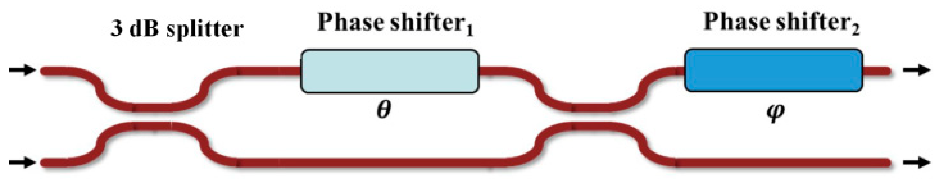
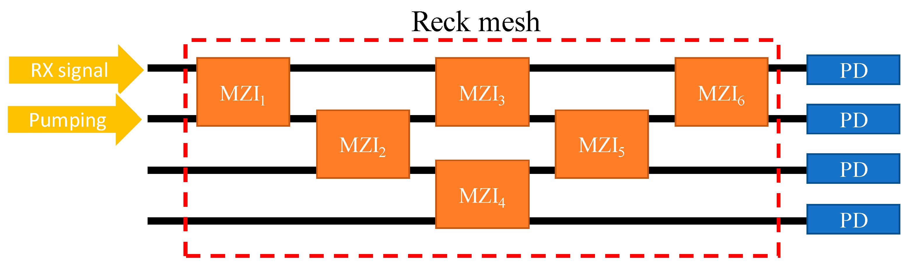
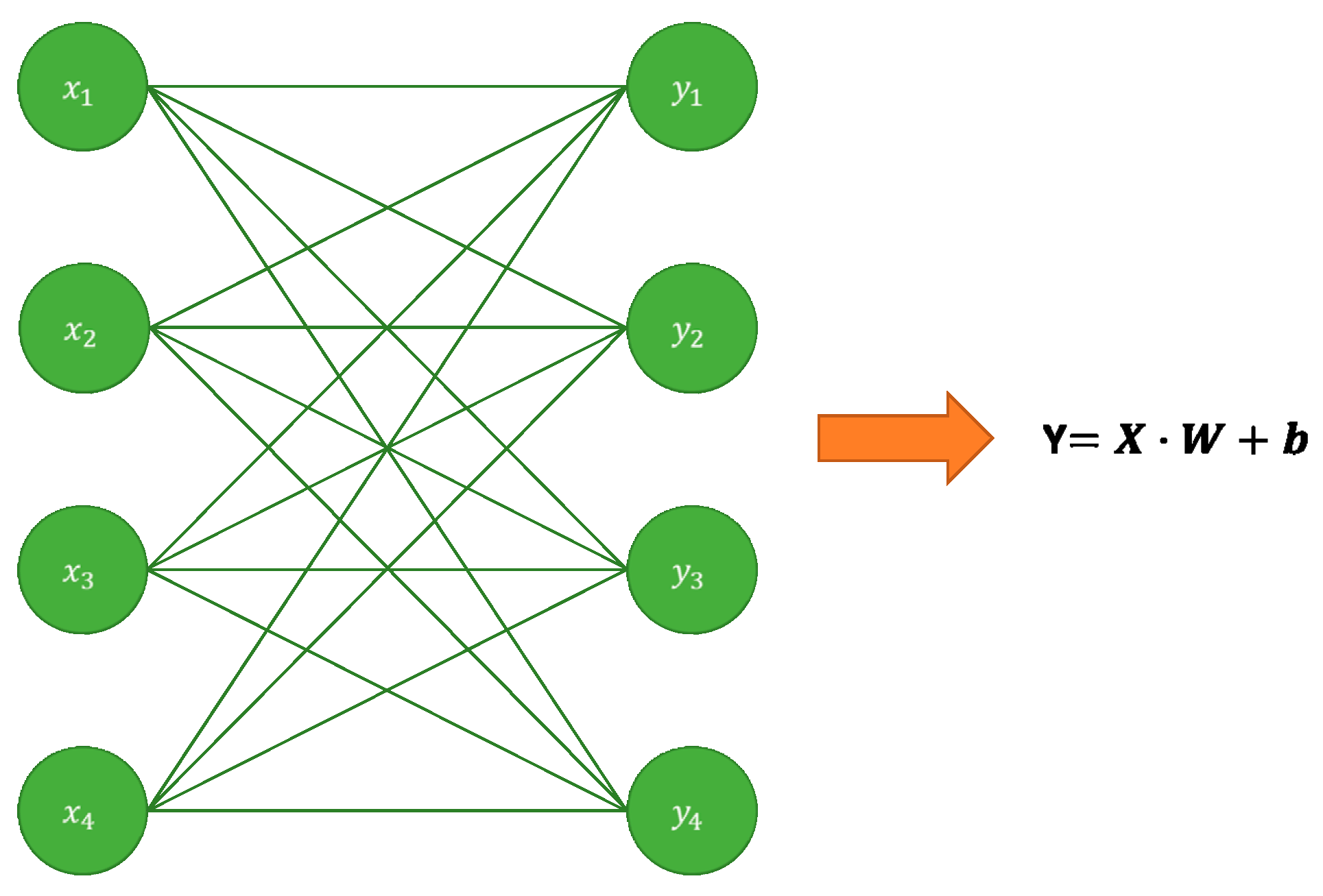
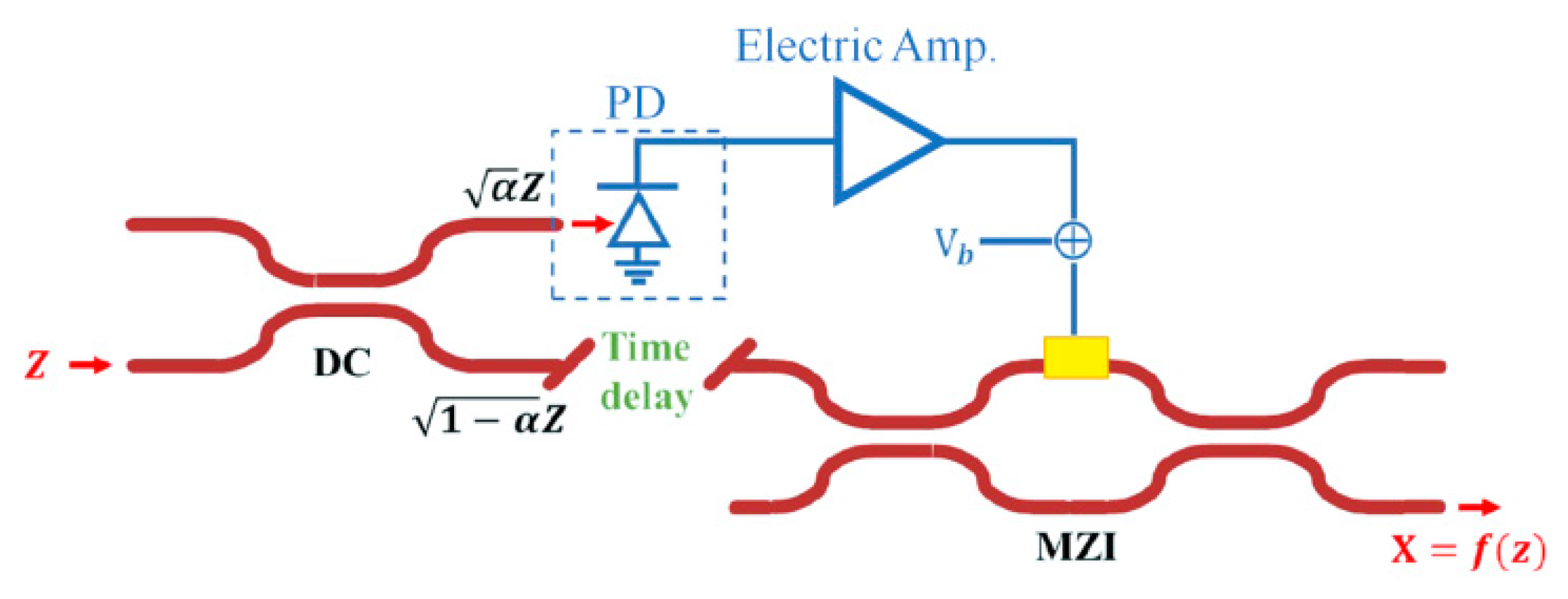
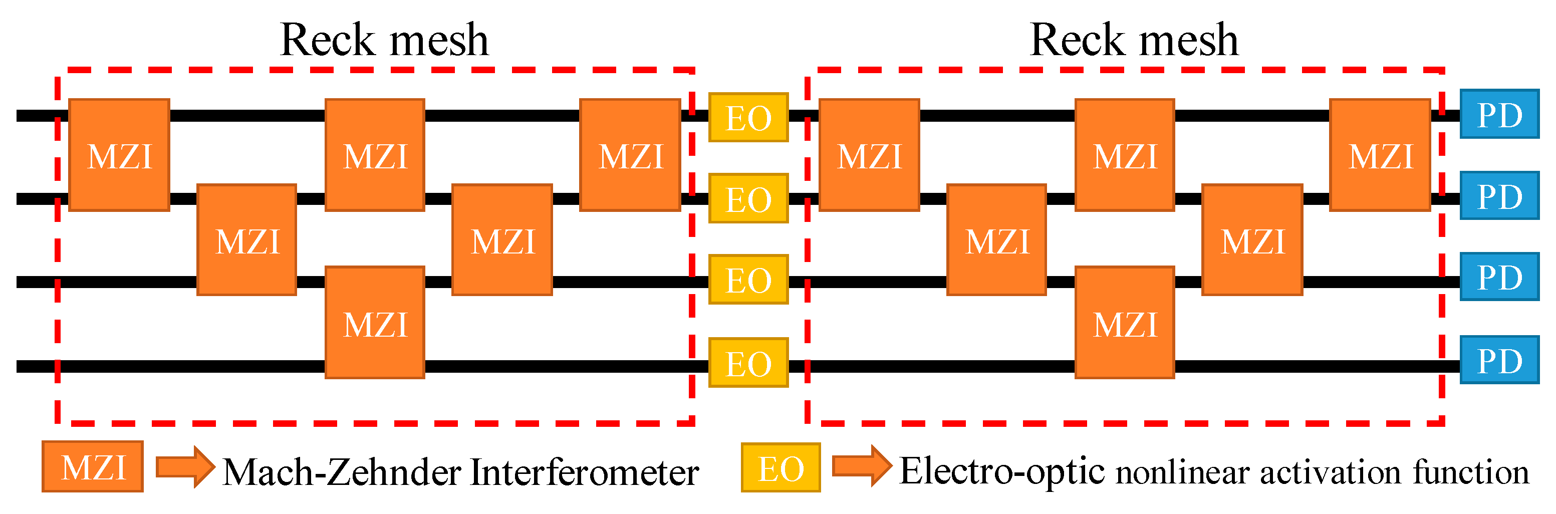
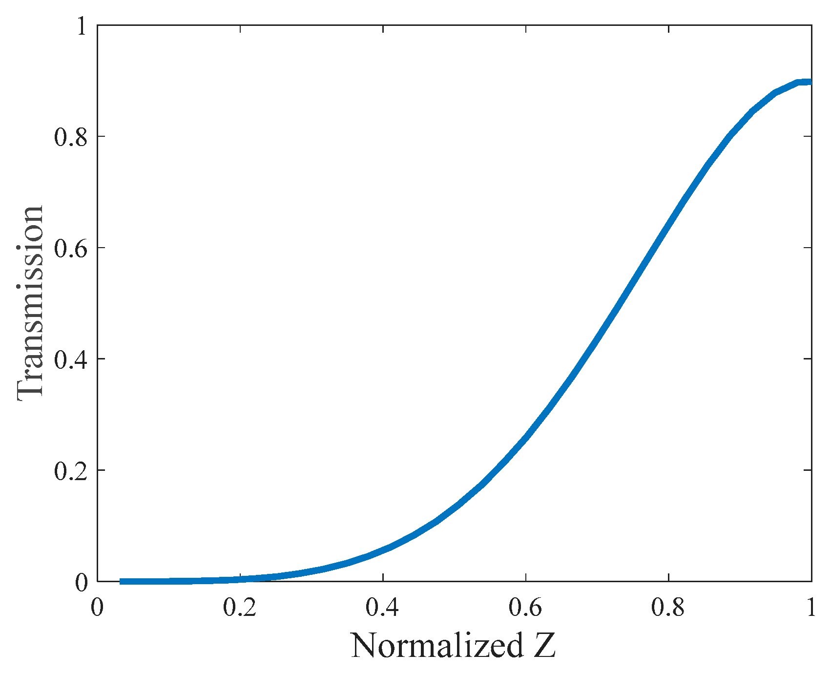
2. Theory of the MZI-Based ONN

The proposed ONN has a multiple MZI configuration achieving a transmission matrix resembles a fully connected layer in a neural network. Figure 1 shows a typical 2 × 2 MZI, which is composed of two 3-dB couplers, a phase shifter θ situated on the top arm inside the MZI, and a phase shifter φ situated at the MZI output. The phase shifter θ controls the MZI output power, while the phase shifter φ determines the phase of the MZI outputs. This configuration permits adaptable rotation within the unitary matrix, thus contributing to its versatility. Equation (1) shows the transformation matrix of MZI, where θ and φ represent the internal and external phase shift values, respectively.
S M Z I = j e j ( θ 2 ) e j φ s i n ( θ 2 ) e j φ c o s ( θ 2 ) c o s ( θ 2 ) s i n ( θ 2 )
Figure 2 shows the architecture of the ONN utilized for the classification of ISI distorted PAM4 signals. This MZI network architecture is known as Reck mesh architecture [32]. The number of MZIs in a N × N Reck mesh is N N 1 2 , where N represents the number of input ports and output ports. These MZIs are organized in (N − 1) rows, with the count of MZIs in each row decreasing from (N − 1) to 1 from top to bottom. The first port is for receiving the PAM4 data, while the second part is for optical pumping. This will be discussed in detail in a later section.
The transformation matrix of each MZI in the mesh can be expanded to a N × N dimensional Hilbert space. Take the 4 × 4 Reck mesh for example, the 4 × 4 dimensional Hilbert space of each MZI is shown in Equations (2)–(4).
D n = S M Z I n 0 0 0 0 0 0 0 0 1 0 0 1   n = 1 ,   3 ,   6
D n = 1 0 0 0 0 0 S M Z I n 0 0 0 0 0 1   n = 2 ,   5
D n = 1 0 0 1 0 0 0 0 0 0 0 0 S M Z I n   n = 4
The S M Z I n   in the equations is the nth MZI transformation matrix as shown in Equation (1). The entire Hilbert space of the network system is derived from the inner product of D n . Therefore, the entire Hilbert space in the Reck mesh can be written as Equation (5). Hence, the input-output relationship of the MZI network can be expressed as Equation (6), where Y represents the output optical field matrix, X is the input optical field matrix, and H denotes the Hilbert space matrix. This operation is like the fully connected layer shown in Figure 3.
H = D 6 · D 5 · D 4 · D 3 · D 2 · D 1
Y = X · H
In a fully connected layer, each connection line from xi to yj can be written as x i   w i , j + b i , j , where w i , j and b i , j are the weight and bias value at connect line, respectively. The relationship between xi and yj is illustrated in Equation (7). Using a matrix to express this relationship, we can obtain Equation (8), where Y is output matrix, X is input matrix, W is weight matrix, and b is the bias matrix. Comparing Equation (8) with Equation (6), it can be observed that they are very similar.
y j = i = 1 i = n x i w i , j + b i , j
Y = X · W + b
Therefore, we can use same way in a neural network like a back-propagation algorithm to optimize H matrix value in the lower loss function value as shown in Equation (9),
H t + 1 = H t α · H t L
where α is the learning rate, is the gradient operator, L is the loss function value, and t is the current epoch. Due to the unitary property inherent in linear transformation matrices, the inverse matrix [SMZI]−1 of each MZI is equal to its conjugate transpose as Equation (10)
S M Z I 1 = j e j ( θ 2 ) e j φ s i n ( θ 2 ) c o s ( θ 2 ) e j φ c o s ( θ 2 ) s i n ( θ 2 )
Hence, the decomposition of H is equivalent to the reverse arrangement of MZIs. This leads to successive products culminating in the eventual formation of the identity matrix as shown in Equation (11). Through the sequential multiplication of H by [Dn]−1 in a defined order, the off-diagonal elements in both the upper and lower triangles of the matrix would eventually become 0. Subsequently, Gaussian elimination can be applied to determine the phase shift values φ and θ at each phase shifter.
H · [ D 1 ] 1 · [ D 2 ] 1 · [ D 3 ] 1 · [ D 4 ] 1 · [ D 5 ] 1 · [ D 6 ] 1 = 1 0 0 0 0 1 0 0 0 0 1 0 0 0 0 1
When the MZI-based ONN has been trained, it can be operated as a PAM4 signal classifier as illustrated in Figure 4. It shows that after the trained MZI-based ONN, different photodiodes (PDs) will be detected corresponding to different levels in the PAM4 input data. However, this part is only the linear operation, and nonlinear activation is needed to handle more complicated scenario.
The nonlinear activation function plays a pivotal role in the functionality of a neural network. In the ONN, one way to achieve nonlinear activation is use the structure shown in Figure 5, which is known as the electro-optic nonlinear activation function [24]. As illustrated in Figure 5, the electro-optic nonlinear activation function structure consists of a directional coupler (DC), a PD, an electric amplifier, and a MZI. In the proposed work, the electrical amplifier is implemented off chip. The DC splitter divides the light into two paths. One pathway receives a fraction α of the input light power, which is then sent to the PD for conversion into an electric signal. In contrast, the remaining fraction of the input light power, which is 1 − α, is directed to the MZI after an appropriate time delay. The PD output voltage will be amplified by the electric amplifier and combined with a proper voltage Vb to input to the MZI phase shift. The operation of electro-optic nonlinear activation function is illustrated in Equation (12), with the two internal components defined in Equations (13) and (14).
f z = j 1 α e j g φ z 2 2 + φ b 2 · cos g φ z 2 2 + φ b 2 z
φ b = π V b V π
g φ = π α G R V π
Above, z is the input light field, α is the DC split power ratio, Vπ is the voltage of the MZI phase shift π, G is the gain of the electric amplifier, and R is the responsivity. Hence, by controlling the Vb, we can conveniently modify Equation (13) to a different nonlinear activation function. By connecting the electro-optic nonlinear activation function in series after the MZI network mesh, a neural network with an activation function can be realized.

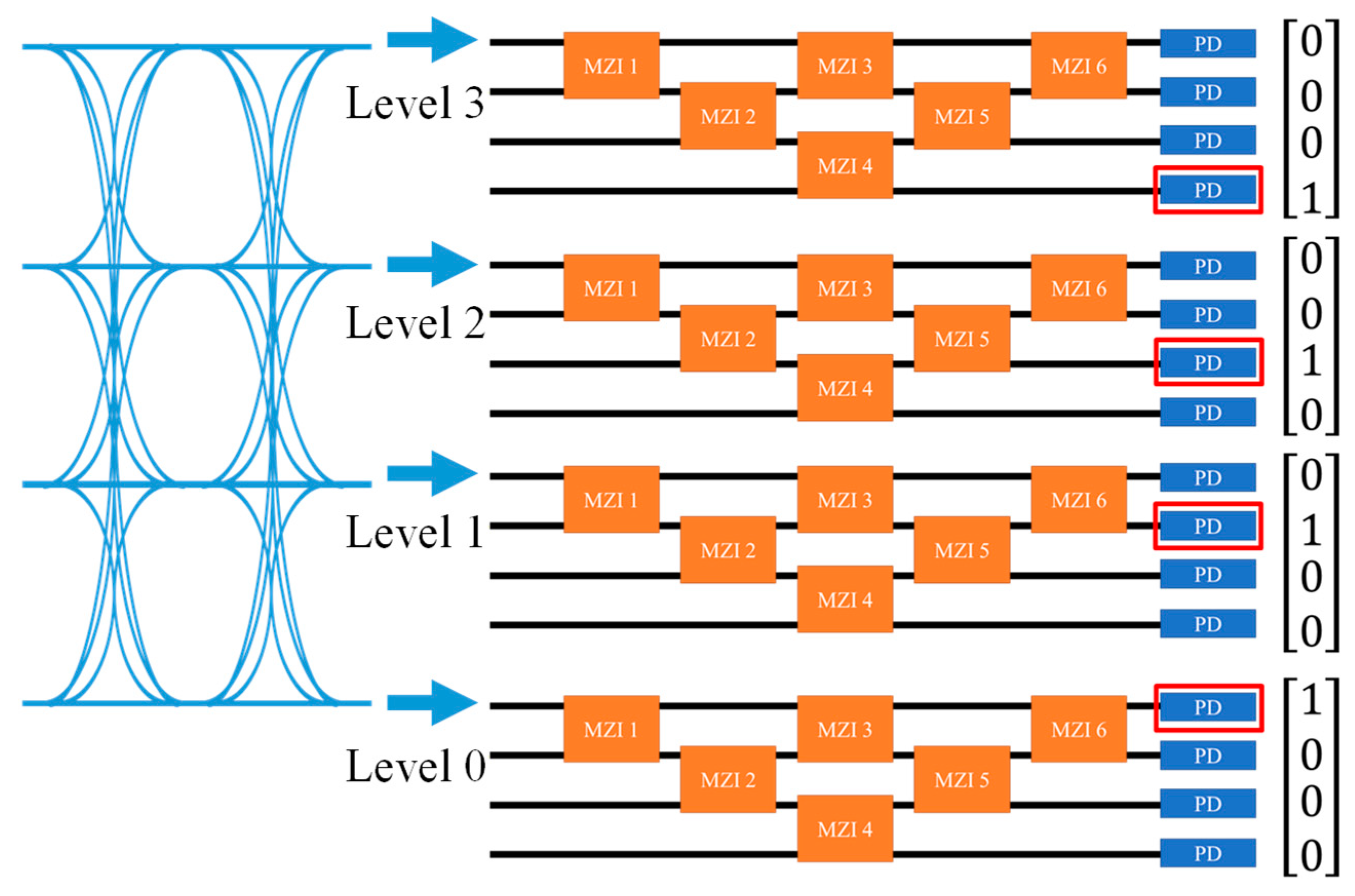
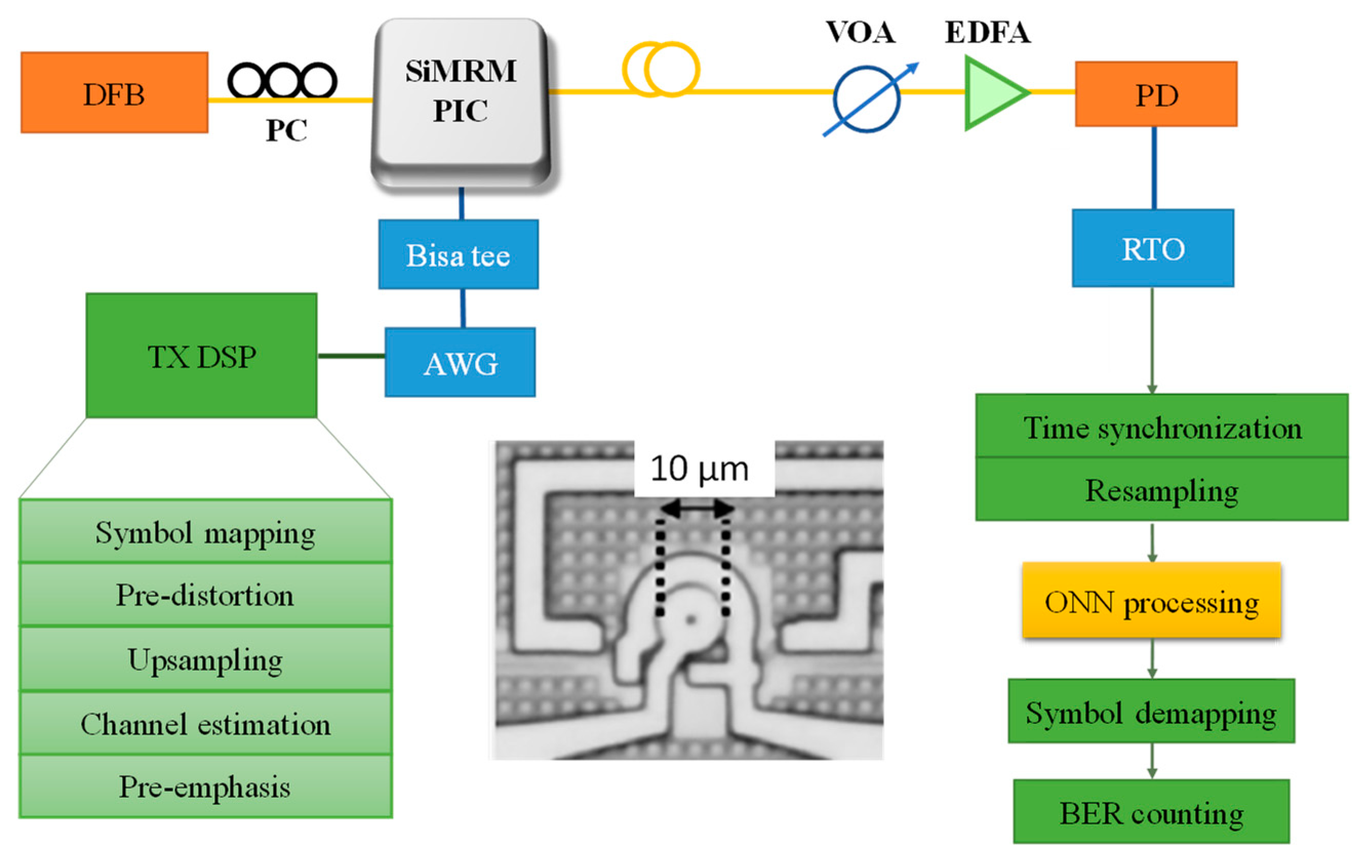
3. Experimental Setup

Figure 6 illustrates the experimental setup to obtain the PAM4 optical signal. At the transmitter (Tx) side, a 1550 nm wavelength distributed feedback (DFB) laser with an output power of 6 dBm is launched into a silicon photonic (SiPh) chip with an SiMRM. The SiMRM was fabricated by the multi-project wafer (MPW) scheme in CUMEC. The electrical PAM4 signal is generated by an arbitrary waveform generator (AWG, Keysight M8194A) with 45 GHz analog bandwidth. Subsequently, the signal is amplified by a 60 GHz radio-frequency (RF) amplifier. The Tx digital signal processing (DSP) includes PAM4 symbol mapping, pre-distortion, upsampling, channel estimation, and pre-emphasis. The pre-distortion and pre-emphasis serve to alleviate non-linear distortion and tackle issues related to high-frequency roll-off, stemming from the limited bandwidth of the AWG. The optical PAM4 signal is produced via a SiMRM with a bandwidth ~67 GHz and operated at −3 V bias, measured by a lightwave component analyzer (LCA; Keysight N4373D). At the receiver (Rx) side, the optical PAM4 signal is detected by a 70 GHz bandwidth PD connected to a real-time oscilloscope (RTO, Keysight UXR0802A) with 80 GHz bandwidth and 256 GSa/s sampling rate. To evaluate transmission performance related to different received optical powers, a variable optical attenuator (VOA) is employed. The Rx DSP invovles time synchronization for ensuring proper alignment of the received signal with the transmitted signal, resampling to adjust the signal sampling rate to match with the neural network, the proposed ONN processing, symbol demapping, and BER evaluation. Inset of Figure 5 shows the photo of the SiMRM with diameter of ~10 μm. It was fabricated on a silicon-on-insulator (SOI) platform with a staring wafer of 220 nm silicon layer and 2 μm buried oxide layer (BOX). The SiMRM has a loaded Q of ~3000.

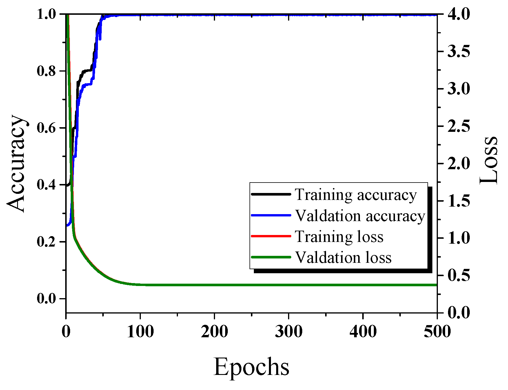
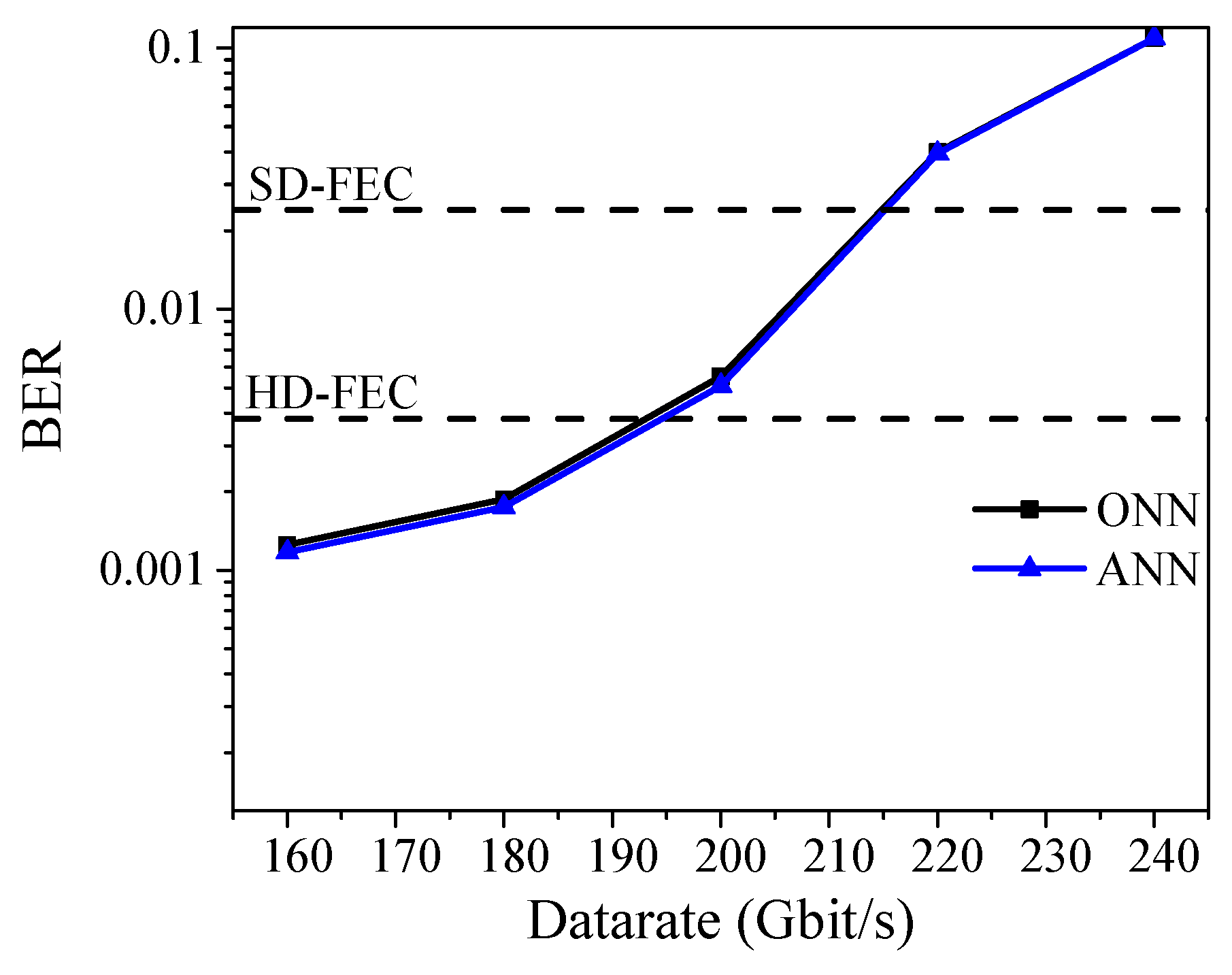
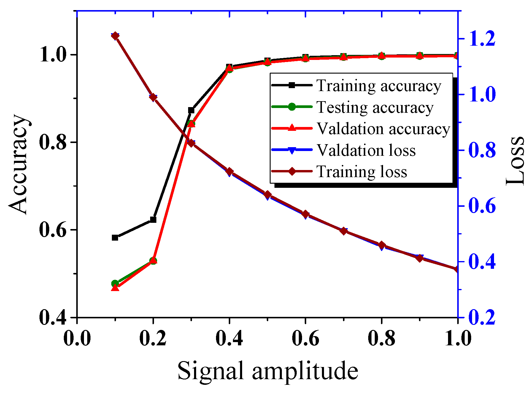
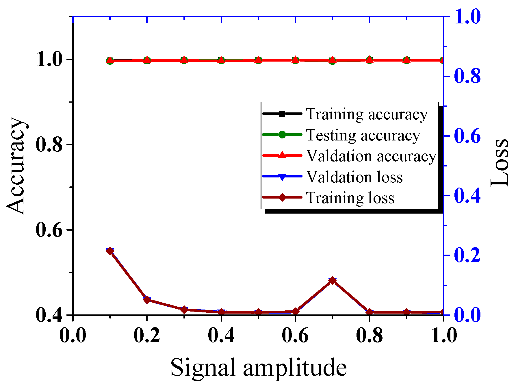
4. Result and Discussion

In this work, we use Neuroptica [33,34], which is a customized ONN simulator programmed in Python to simulate the PAM4 signal classify by ONN processing. As discussed above, Figure 2 shows the architecture of a Reck-based ONN to classify the experimentally obtained PAM4 signal. We only use two ports for the classification of the distorted PAM4 signal as indicated in Figure 2. The first port is for receiving the PAM4 data, while the second part is for optical pumping. In this work, the optical pumping is needed to increase signal resolvability and provide additional optical power to amplify the PAM4 data. Similar to the case of coherent detection, the pumping light can amplify the optical signal like the local oscillator (LO) light. Here, we did not consider the additional noise of pumping light in our simulation. However, the influence of additional noise from pumping light on the system will be similar to that of a coherent transmission system. To simulate the PD, a square law detection is implemented at the output ports. The classification result depends on the maximum element in the output matrix. Therefore, the target data should be processed by one-hot encode. To update the ONN parameters, cross-entropy loss function is employed, and the optimizer is the Adam. In order to evaluate the performance of proposed ONN, a fully connected ANN using traditional computer simulation is also performed for comparison. This ANN has a four by four fully connected layer with the ReLU activation function. As the ANN is used to compare with the proposed ONN, it has the same number of neurons as the ONN. Hence, it will theoretically have the same performance as the ONN. The dataset used is experimental data obtained from our previous work in [29]. The received waveforms are adjusted by resampling so that there is one sample per symbol. The data length of each transmission data rate experiment is 217 bauds. We use 20% data for training and 80% for testing. In the proof-of-concept demonstration illustrated in Figure 6, the input data are experimentally generated by a bandwidth-limited SiMRM chip. This experimental ISI-distorted optical PAM4 signal will be detected by a separated PD, and a RTO will store the electrical PAM4 signal as shown in Figure 6. Hence, this stored electrical PAM4 signal can be used for the ONN simulation. In the future ONN chip implementation, the ISI distorted optical PAM4 signal can be directly launched into the ONN chip “RX signal” port as shown in Figure 2; hence, no additional OE conversion by the PD is needed. In this case, four on-chip PDs on the ONN chip are used as shown in Figure 2. The optical amplification can be realized by the pumping light as discussed before; hence, VOA and EDFA may not be necessary. Figure 7 shows the accuracy and loss curves for the proposed ONN. It is evident from the results that the ONN exhibits convergence at approximately 100 epochs.
Figure 8 illustrates the BER performance of PAM4 signals utilizing both the proposed ONN and ANN. The ONN can recover and classify distorted PAM4 signals within the range of 160 Gbit/s to 240 Gbit/s (i.e., 80 GBaud to 120 GBaud). The data rate achieving the SD-FEC threshold (i.e., BER = 2.4 × 10⁻²) can be up to 200 Gbit/s.
It is worth noting that the proposed ONN without an activation function is particularly sensitive to signal power variations. When the signal power is low, the accuracy of the model tends to decrease significantly. Figure 9 illustrates the accuracy and loss performance of different normalized input signal amplitudes. For better understanding, here, the normalized signal amplitude represents the first level of the PAM4 signal, and the four levels in the PAM4 have the same separation. Taking the signal amplitude of 0.8 as an example, the PAM4 values would be 0.8, 1.6, 2.4 and 3.2. We can observe from Figure 9 that the accuracy and loss performance are poor when the normalized input signal amplitude is lower than 0.6. At the normalized input signal of 0.1, the model accuracy falls below 50%. According to our simulation results, the ONN accuracy reduces when the signal amplitude is less than 0.4. This happens because when the signal amplitude is too low, the ASE noise from the EDFA and the thermal and shot noises from the PD become dominant, causing the ONN to fail in performing classification and prediction. When the signal amplitude is larger than 0.4, the ASE and PD noises will not be the dominating factors, and we can observe that the ONN accuracy is ~1 when signal amplitude is between 0.6 and 1.0. To solve this issue, the electro-optic nonlinear activation function discussed in Figure 5 above is included into the ONN model. This enhances the capability of the ONN model to handle nonlinear problems.
Figure 10 shows the modified ONN model with electro-optic nonlinear activation functions. In this architecture, each output port of the first Reck mesh will be connected to an electro-optic nonlinear activation function. The output of the electro-optic nonlinear activation function will then be connected to the input port of the second Reck mesh, and subsequently will be connected to a PD. Furthermore, the fusion of the activation function and the fully connected layer can be considered as a two-layer fully connected ONN, interconnected through activation functions
In the modified ONN, the parameters of the electro-optic nonlinear activation function as optimized. The α is set to be 0.1, Vπ of the MZI phase shift is 5 V, the Vb is set to be −5 V, G is set to be 20, and the responsivity R is set to be 1. Therefore, φ b is set to be -π, and g φ is set to be 0.4π. Figure 11 shows the transmission coefficient (i.e., f z 2 z 2 ) of the electro-optic nonlinear activation function with normalized input field Z. We can observe that the electro-optic nonlinear activation function defined exhibits similarities to the sigmoid function but shifted towards the positive x-axis. In the simulation work here, the α = 0.1 is used for reducing the loss for electro-optic nonlinear activation function. The electro-optic nonlinear activation function will have different characteristics under different φ b and g φ . Here, we found that the nonlinear activation function as illustrated in Figure 11 has a better performance in our model. Therefore, φ b is set to be −π, and g φ is set to be 0.4π.
Figure 12 illustrates the accuracy and loss performance of different normalized input signal amplitudes with the electro-optic nonlinear activation function. Comparing the results to the ONN model without an electro-optic nonlinear activation function shown in Figure 10, the accuracy and loss performance in Figure 12 have been significantly improved, particularly at low input signal powers. We can observe that even when the normalized input signal amplitude is as low as 0.1, the accuracy remains at an impressive value of 99.7%.
Analyzing the BER performance of PAM4 signals involves using the modified ONN with an electro-optic nonlinear activation function. It can be observed that the BER performance of the modified ONN model with the electro-optic nonlinear activation function is nearly the same as that without the activation function illustrated in Figure 8. The data rate achieving the SD-FEC threshold (i.e., BER = 2.4 × 10⁻²) can be up to 200 Gbit/s. This reveals that when the input signal power is high enough, no additional bit error will be introduced for the ONN without the electro-optic nonlinear activation function. However, the introduction of activation function increases the robustness of the proposed ONN. We analyze the impact of the phase shift error on MZI ONN performance. To simulate the phase error of phase shift, we introduce a random normal distribution N 0 , σ 2 and add it to the final training results of the phase shift value for each phase shifter in the MZIs. Here, σ is the standard deviation of the phase error. Therefore, the θ and φ in Equation (1) are now written as θ ^ and φ ^   as shown in Equations (15) and (16).
θ ^ = θ + N 0 , σ 2
φ ^ = φ + N 0 , σ 2
Then, we analyze the impact of the phase error on the ONN. Figure 13 shows the BER performance under various standard deviation phase errors at a data rate of 160 Gbit/s. Here, each BER point is obtained by averaging 1000 BER calculations to ensure the randomness. By analyzing phase errors from 0° to 1.5°, we can observe that the BER performance remains within the SD-FEC threshold when the standard deviation of phase errors is up to 1°. In Figure 13, we also compare the BER performance of the ONN model with and without electro-optic nonlinear activation function under different standard deviation phase errors. Under 1° phase error, the ONN model with electro-optic nonlinear activation function achieves a slightly lower Bit Error Rate (BER) compared to the standard deviation phase errors. This shows the ONN model with the electro-optic nonlinear activation function possesses a higher tolerance for phase errors, providing a more stable and reliable performance under 1° of phase error.

5. Conclusions

We proposed and demonstrated an ONN to regenerate PAM4 signal with high ISI generated experimentally by a SiMRM. As the SiMRM has a 3-dB modulation bandwidth of ~67 GHz, the expected PAM4 data rate is ~134 Gbit/s (i.e., 2 bit/symbol × 67 Gbaud). When the data rate is operated at >200 Gbit/s, the generated PAM4 optical signal suffers from severe ISI. The proposed ONN has a multiple MZI configuration achieving a transmission matrix that resembled a fully connected layer in a neural network. The PAM4 signals at data rates from 160 Gbit/s to 240 Gbit/s (i.e., 80 GBaud to 120 GBaud) were experimentally generated using a SiMRM with limited modulation bandwidth of ~67 GHz. The proposed ONN is performed via Neuroptica, which is a customized ONN simulator programmed in Python. Results showed that SD-FEC requirement (i.e., BER < 2.4 × 10⁻²) can be achieved at 200 Gbit/s transmission, and the proposed ONN has nearly the same performance with ANN implemented using traditional computer simulation. Moreover, we also discussed the effect of electro-optic nonlinear activation function on the ONN model. By comparing the ONN model with and without electro-optic nonlinear activation function in different input signal amplitudes, it can be observed that the accuracy and loss can be significantly improved at low input signal amplitudes. Even at the normalized input signal amplitude of 0.1, the accuracy can still achieve 99.7%. Furthermore, we analyzed the impact of the phase shift error of MZI to the ONN model. Both ONN model with and without electro-optic nonlinear activation function can still achieve SD-FEC threshold under a 1° phase shift error.

Author Contributions

All authors contributed to the study conception and design. Data collection and analysis were performed by T.-Y.H., D.W.U.C. and C.-W.P. The first draft of the manuscript was written by T.-Y.H. All authors have read and agreed to the published version of the manuscript.

Funding

This work was supported by National Science and Technology Council, Taiwan, under Grant NSTC-112-2221-EA49-102-MY3, NSTC-112-2218-E-011-006, NSC-112-3111-E-A49-001, NSTC-110-2221-E-A49-057-MY3.

Institutional Review Board Statement

Not applicable.

Informed Consent Statement

Not applicable.

Data Availability Statement

The data presented in this study are available on request from the corresponding author.

Conflicts of Interest

The authors declare no conflicts of interest.

References

  1. Soref, R.; Dong, P.; Chen, J.; Melikyan, A.; Fan, T.; Fryett, T.; Li, C.; Chen, J.; Koeppen, C. Silicon photonics for 800G and beyond. In Proceedings of the Optical Fiber Communication Conference; Optica Publishing Group: San Diego, CA, USA, 2022; p. M4H-1. [Google Scholar]
  2. 800G Pluggable MSA Group. 2022. Available online: https://www.800gmsa.com/ (accessed on 7 April 2024).
  3. Available online: https://www.marvell.com/company/newsroom/marvell-extends-connectivity-leadership-with-industrys-first-pam4-optical-dsp.html (accessed on 7 April 2024).
  4. Zhou, X.; Urata, R.; Liu, H. Beyond 1 Tb/s intra-data center interconnect technology: IM-DD OR coherent? J. Light. Technol. 2020, 38, 475–484. [Google Scholar] [CrossRef]
  5. Ozolins, O.; Joharifar, M.; Salgals, T.; Louchet, H.; Schatz, R.; Gruen, M.; Dippon, T.; Kruger, B.; Pittala, F.; Che, D.; et al. Optical amplification-free high baudrate links for intra-data center communications. J. Light. Technol. 2023, 41, 1200–1206. [Google Scholar] [CrossRef]
  6. Malik, A.; Liu, S.; Timurdogan, E.; Harrington, M.; Netherton, A.; Saeidi, M.; Blumenthal, D.J.; Theogarajan, L.; Watts, M.; Bowers, J.E. Low power consumption silicon photonics datacenter interconnects enabled by a parallel architecture. In Proceedings of the Optical Fiber Communication Conference; Optica Publishing Group: San Francisco, CA, USA, 2021; p. W6A-3. [Google Scholar]
  7. Zhou, J.; Wang, J.; Zhu, L.; Zhang, Q. Silicon photonics for 100Gbaud. J. Light. Technol. 2021, 39, 857–867. [Google Scholar] [CrossRef]
  8. Ahmed, A.H.; Sharkia, A.; Casper, B.; Mirabbasi, S.; Shekhar, S. Silicon-photonics microring links for datacenters—Challenges and opportunities. IEEE J. Sel. Top. Quant. Electron. 2016, 22, 194–203. [Google Scholar] [CrossRef]
  9. Peng, C.W.; Chow, C.W.; Kuo, P.C.; Chen, G.H.; Yeh, C.H.; Chen, J.; Lai, Y. DP-QPSK coherent detection using 2D grating coupled silicon based receiver. IEEE Photonics J. 2021, 13, 7900105. [Google Scholar] [CrossRef]
  10. Rahim, A.; Hermans, A.; Wohlfeil, B.; Petousi, D.; Kuyken, B.; Van Thourhout, D.; Baets, R.G. Taking silicon photonics modulators to a higher performance level: State-of-the-art and a review of new technologies. Adv. Photonics 2021, 3, 024003. [Google Scholar] [CrossRef]
  11. Luo, L.W.; Ophir, N.; Chen, C.P.; Gabrielli, L.H.; Poitras, C.B.; Bergmen, K.; Lipson, M. WDM-compatible mode-division multiplexing on a silicon chip. Nat. Comm. 2014, 5, 3069. [Google Scholar] [CrossRef]
  12. Zhang, F.; Zhang, L.; Ruan, X.; Yang, F.; Ming, H.; Li, Y. High baud rate transmission with silicon photonic modulators. IEEE J. Sel. Top. Quantum Electron. 2021, 27, 8300709. [Google Scholar] [CrossRef]
  13. Dourado, D.M.; de Farias, G.B.; Gounella, R.H.; Rocha, M.D.L.; Carmo, J.P. Challenges in silicon photonics modulators for data center interconnect applications. Opt. Laser Technol. 2021, 144, 107376. [Google Scholar] [CrossRef]
  14. Hsu, Y.; Tzu, T.C.; Lin, T.C.; Chuang, C.Y.; Wu, X.; Chen, J.; Yeh, C.H.; Tsang, H.K.; Chow, C.W. 64-Gbit/s PAM-4 20-km transmission using silicon micro-ring modulator for optical access networks. In Proceedings of the Optical Fiber Communication Conference; Optica Publishing Group: Los Angeles, CA, USA, 2017; p. M3H.2. [Google Scholar]
  15. Chan, D.W.U.; Wu, X.; Lu, C.; Lau, A.P.T.; Tsang, H.K. Efficient 330-Gb/s PAM-8 modulation using silicon microring modulators. Opt. Lett. 2023, 48, 1036–1039. [Google Scholar] [CrossRef]
  16. Hung, T.Y.; Chan, D.W.U.; Peng, C.W.; Chow, C.W.; Tsang, H.K. 300-Gbit/s/λ 8-Level pulse-amplitude-modulation (PAM8) with a silicon microring modulator utilizing long short term memory regression and deep neural network classification. Opt. Laser Technol. 2024, 171, 110379. [Google Scholar] [CrossRef]
  17. Deligiannidis, S.; Mesaritakis, C.; Bogris, A. Performance and complexity evaluation of recurrent neural network models for fibre nonlinear equalization in digital coherent systems. In Proceedings of the 2020 European Conference on Optical Communications (ECOC), Brussels, Belgium, 6–10 December 2020; pp. 1–4. [Google Scholar] [CrossRef]
  18. Hung, N.T.; Stainton, S.; Le, S.T.; Haigh, P.A.; Tien, H.P.; Vien, N.D.N.; Tuan, N.V. High-speed PAM4 transmission using directly modulated laser and artificial neural network nonlinear equalizer. Opt. Laser Technol. 2023, 157, 108642. [Google Scholar] [CrossRef]
  19. Wang, C.; Du, J.; Chen, G.; Wang, H.; Sun, L.; Xu, K.; Liu, B.; He, Z. QAM classification methods by SVM machine learning for improved optical interconnection. Opt. Comm. 2019, 444, 1–8. [Google Scholar] [CrossRef]
  20. Shastri, B.J.; Tait, A.N.; de Lima, T.F.; Pernice, W.H.P.; Bhaskaran, H.; Wright, C.D.; Prucnal, P.R. Photonics for artificial intelligence and neuromorphic computing. Nat. Photonics 2021, 15, 102–114. [Google Scholar] [CrossRef]
  21. Tait, A.N.; de Lima, T.F.; Zhou, E.; Wu, A.X.; Nahmias, M.A.; Shastri, B.J.; Prucnal, P.R. Neuromorphic photonic networks using silicon photonic weight banks. Sci. Rep. 2017, 7, 7430. [Google Scholar] [CrossRef]
  22. Liao, K.; Dai, T.; Yan, Q.; Hu, X.; Gong, Q. Integrated photonic neural networks: Opportunities and challenges. ACS Photonics 2023, 10, 2001–2010. [Google Scholar] [CrossRef]
  23. Zhang, D.; Tan, Z. A review of optical neural networks. App. Sci. 2022, 12, 5338. [Google Scholar] [CrossRef]
  24. Zhou, T.; Lin, X.; Wu, J.; Chen, Y.; Xie, H.; Li, Y.; Wu, H.; Fang, L.; Dai, Q. Large-scale neuromorphic optoelectronic computing with a reconfigurable diffractive processing unit. Nat. Photonics 2021, 15, 367–373. [Google Scholar] [CrossRef]
  25. Shokraneh, F.; Geoffroy-Gagnon, S.; Nezami, M.S.; Liboiron-Ladouceur, O. A single layer neural network implemented by a 4 × 4 MZI-based optical processor. IEEE Photonics J. 2019, 11, 4501612. [Google Scholar] [CrossRef]
  26. Mojaver, K.R.; Zhao, B.; Leung, E.; Safaee, S.M.R.; Liboiron-Ladouceur, O. Addressing the programming challenges of practical interferometric mesh based optical processors. Opt. Exp. 2023, 31, 23851–23866. [Google Scholar] [CrossRef]
  27. Ma, X.; Peserico, N.; Shastri, B.J.; Sorger, V.J. Design and testing of a Silicon Photonic Tensor Core with integrated lasers. In Proceedings of the 2023 IEEE Silicon Photonics Conference (SiPhotonics), Washington, DC, USA, 4–7 April 2023; pp. 1–2. [Google Scholar] [CrossRef]
  28. Teo, T.Y.; Ma, X.; Pastor, E.; Wang, H.; George, J.K.; Yang, J.K.W.; Wall, S.; Miscuglio, M.; Simpson, R.E.; Sorger, V.J. Programmable chalcogenide-based all-optical deep neural networks. Nanophotonics 2022, 11, 4073–4088. [Google Scholar] [CrossRef]
  29. Chan, D.W.U.; Wu, X.; Zhang, Z.; Lu, C.; Lau, A.P.T.; Tsang, H.K. C-band 67 GHz silicon photonic microring modulator for dispersion-uncompensated 100 Gbaud PAM-4. Opt. Lett. 2022, 47, 2935–2938. [Google Scholar] [CrossRef]
  30. Wu, H.W.; Lu, H.H.; Tsai, W.S.; Huang, Y.C.; Xie, J.Y.; Huang, Q.P.; Tu, S.C. A 448-Gb/s PAM4 FSO communication with polarization-multiplexing injection-locked VCSELs through 600 m free-space link. IEEE Access 2020, 8, 28859–28866. [Google Scholar] [CrossRef]
  31. Tsai, W.S.; Li, C.Y.; Lu, H.H.; Lu, Y.F.; Tu, S.C.; Huang, Y.C. 256 Gb/s four-channel SDM-based PAM4 FSO-UWOC convergent system. IEEE Photon. J. 2019, 11, 7902008. [Google Scholar] [CrossRef]
  32. Reck, M.; Zeilinger, A.; Bernstein, H.J.; Bertani, P. Experimental realization of any discrete unitary operator. Phys. Rev. Lett. 1994, 73, 58. [Google Scholar] [CrossRef]
  33. Williamson, I.A.D.; Hughes, T.W.; Minkov, M.; Bartlett, B.; Pai, S.; Fan, S. Reprogrammable electro-optic nonlinear activation functions for optical neural networks. IEEE J. Sel. Top. Quantum Electron. 2020, 26, 7700412. [Google Scholar] [CrossRef]
  34. Bartlett, B.; Minkov, M.; Hughes, T.; Williamson, I.A.D. Neuroptica: Flexible Simulation Package for Optical Neural Networks, GitHub Repository. 2019. Available online: https://github.com/fancompute/neuroptica (accessed on 7 April 2024).
Figure 1. A typical 2 × 2 MZI used in the ONN. It consists of two 3-dB couplers, a phase shifter θ=, and a phase shifter φ.
Photonics 11 00349 g001
Figure 2. The architecture of MZI-based ONN in Reck mesh architecture.
Photonics 11 00349 g002
Figure 3. The 4 × 4 fully connected layer neural network operation.
Photonics 11 00349 g003
Figure 4. After proper training, the MZI-based ONN is acted as a PAM4 signal classifier.
Photonics 11 00349 g004
Figure 5. The structure of electro-optic nonlinear activation functions. MZI: Mach–Zehnder Interferometer; DC: directional coupler; PD: photodetector.
Photonics 11 00349 g005
Figure 6. The experimental setup to obtain the PAM4 optical signal. AWG: arbitrary waveform generator; DFB: distributed feedback laser diodes; PC: polarization controller; EDFA: erbium-doped fiber amplifier; VOA: variable optical attenuator; PD: photodetector; RTO: real-time oscilloscope. Inset: photo of the SiMRM.
Photonics 11 00349 g006
Figure 7. The accuracy and loss curves for the proposed ONN.
Photonics 11 00349 g007
Figure 8. BER performances of ONN and ANN used for classifying the distorted PAM4 signal without the activation function.
Photonics 11 00349 g008
Figure 9. Accuracy and loss performance of different normalized input signal amplitudes without activation function.
Photonics 11 00349 g009
Figure 10. Modified ONN model with electro-optic nonlinear activation functions. MZI: Mach–Zehnder Interferometer; EO: electro-optic nonlinear activation function; PD: photodetector.
Photonics 11 00349 g010
Figure 11. Modified ONN model with electro-optic nonlinear activation functions.
Photonics 11 00349 g011
Figure 12. Accuracy and loss performance of different normalized input signal amplitudes with an activation function.
Photonics 11 00349 g012
Figure 13. BER performance under various standard deviation phase errors at a data rate of 160 Gbit/s.
Photonics 11 00349 g013
Disclaimer/Publisher’s Note: The statements, opinions and data contained in all publications are solely those of the individual author(s) and contributor(s) and not of MDPI and/or the editor(s). MDPI and/or the editor(s) disclaim responsibility for any injury to people or property resulting from any ideas, methods, instructions or products referred to in the content.

