Article

Dynamic Polarization Patterning Technique for High-Quality Liquid Crystal Planar Optics

1
School of Optoelectronic Science and Engineering & Collaborative Innovation Center of Suzhou Nano Science and Technology, Soochow University, Suzhou 215006, China
2
Key Lab of Advanced Optical Manufacturing Technologies of Jiangsu Province & Key Lab of Modern Optical Technologies of Education Ministry of China, Soochow University, Suzhou 215006, China
*
Author to whom correspondence should be addressed.
Photonics 2024, 11(4), 350; https://doi.org/10.3390/photonics11040350
Submission received: 27 February 2024 / Revised: 15 March 2024 / Accepted: 8 April 2024 / Published: 10 April 2024
(This article belongs to the Section Optoelectronics and Optical Materials)

Abstract

:
The Pancharatnam–Berry (PB)-phase liquid crystal (LC) planar optical elements, featuring large apertures and a light weight, are emerging as the new generation optics. The primary method for fabricating large-aperture LC planar optical elements is through photo-alignment, utilizing polarization laser direct writing. However, conventional polarization direct writing suffers from an inertia-induced stopping step during splicing, leading to suboptimal optical effects. Here, we propose a novel highly efficient method for arbitrary polarization patterning, significantly reducing interface splicing errors in these optical elements. (We call it dynamic polarization patterning technology). This process involves simultaneous mobile splicing and real-time generation of different polarization patterns for exposure, eliminating the inertia-related splicing interruption. As a demonstration, we fabricated a lens with an aperture of approximately 1 cm within 30 min at 633 nm. Furthermore, we developed a 100% fill-factor lens array (3 × 3) with an element lens diameter of approximately 7 mm within 1.5 h at 532 nm. Their focal lengths were uniformly set at 30 cm, demonstrating superior convergence capabilities within their designated working wavelengths, alongside commendable performance in converging light across various other wavelengths. Our measurements confirmed the good focusing performance of these samples. The convergence spot size of the lens deviated by approximately 40% from the theoretical diffraction limit, whereas the lens array exhibited a deviation of around 30%. The dynamic polarization direct writing during uniform platform movement reduced splicing errors to a mere 100–200 nm. The enhancement in imaging quality can be primarily attributed to the innovative use of mobile polarization splicing exposure technology, coupled with the inherent self-smoothing properties of LC molecules. This synergy significantly mitigates the impact of seam diffraction interference.

1. Introduction

The PB phase-based LC planar optical elements, including polarization gratings [1,2,3], LC lenses [4,5,6,7], vortex sheets [8,9], etc., are considered the fourth generation of optical devices [10,11,12,13,14,15,16]. Benefiting from the advantages of large apertures, a light weight, thin thickness, and stimuli tunability [11,17], these elements have promoted the development of technologies such as fingerprint recognition [18,19], virtual reality and augmented reality [20,21], polarization imaging [22,23], and beam control [24,25]. There are methods for producing LC planar optical devices, such as polarization holography [26,27,28,29], polarization projection lithography [30,31], and polarization laser direct writing [32,33,34]. However, the size of the devices manufactured using holographic and projection lithography is inherently limited. This is because the size of the devices they fabricate is frequently constrained by the dimensions of the optical system components, resulting in significant costs associated with the production of larger-diameter elements. Consequently, the components they produce are typically limited to a few millimeters in size. Laser direct writing, also known as polarization direct writing, has emerged as a primary means of fabricating LC planar optical components, particularly those with larger diameters [35]. However, conventional polarization direct writing methods often encounter inertial stop splicing steps during device fabrication, leading to suboptimal optical performance in the produced components. Since the optical properties are highly sensitive to splicing errors, given the proximity of the splicing size to the optical wavelength, it is imperative to minimize the splicing interference as much as possible. Ideally, a method that allows for continuous machine operation during the splicing process would eliminate the inertia-induced stoppages, thereby enhancing the performance of the manufactured devices.
In this study, we introduce a dynamic polarization patterning exposure technique, which is characterized by high efficiency and flexibility. The aim of this technique is to mitigate the splicing errors typically encountered in traditional laser direct writing due to inertia. Our approach involves generating a surface profile using the Fresnel lens formula and then employing this profile as a dynamic mask during system operation. This enables the system to generate a mask in real time via a Digital Micromirror Device (DMD) during movement, eliminating the need for inertial stop splicing steps, thus significantly reducing splicing errors. The splicing errors between the lens and lens array prepared using this method are only within the range of 100–200 nm, demonstrating excellent focusing capability and near-diffraction-limit performance. This breakthrough opens up new possibilities for fabricating high-quality LC photonic devices.

2. Experimental Details

The system employed in this study, as depicted in Figure 1a,b, operates in a highly dynamic and efficient way. Starting from the initial point, the system quickly proceeds to the next starting point upon completing the exposure of a polarization pattern. Concurrently, it adjusts the laser polarization angle to expose the following pattern. This mobile splicing process is executed seamlessly, due to the predefined lens phase profile file and the real-time generation of distinct polarization patterns by the DMD. This approach eliminates inertia-induced stoppages during the splicing step, thereby minimizing splicing errors. In Figure 1b, we illustrate a hypothetical scenario, where the production of a lens is divided into three distinct steps. Beginning at the first starting point, the DMD generates a real-time mask for the initial step of exposure. Once this exposure is completed, the system swiftly transitions to the second starting point. At this juncture, the system commands the laser to adjust its polarization angle, while the DMD simultaneously produces a mask for the second step of exposure. This process is repeated for the third step, marking the conclusion of one exposure cycle. This cycle is then repeated for the subsequent steps until the sample is fully completed. The continuous motion of the system throughout the exposure process ensures the absence of inertia-induced stoppages, thereby significantly reducing splicing errors. This innovative approach not only enhances the precision and quality of the produced lenses but also paves the way for more efficient and reliable optical component manufacturing techniques.
The low-error polarization direct writing system comprises several key components, including the polarization control module, miniature imaging splicing module, automatic focusing module, and other system elements. As depicted in Figure 2, the 355 nm light emitted by the laser first passes through the beam expander and collimator before entering the polarization control module. Within this module, a linear polarizer enhances the polarization of the light source, while a half-wave plate adjusts the polarization angle of the laser. By leveraging the characteristics of the half-wave plate, a change in the α angle results in a linearly polarized light shift of the 2α angle, enabling the DMD to generate dynamic masks in real time. This polarization control module enables dynamic generation of polarization patterns at any angle, aligned with our experimental design. Subsequently, the beam traverses through the beam splitter, with a portion directed onto the Charge-Coupled Device (CCD) for the real-time monitoring of spot images on the computer. The remaining portion enters the miniature imaging splicing module, where it undergoes miniaturization via the objective lens before being incident on the prepared sample. Some of the light is reflected into the focusing module, which employs a servo focusing system to dynamically adjust the focal length in real time. Throughout the entire process, the machine moves concurrently with the exposure process, owing to the system’s ability to synchronize and control the aforementioned modules in real time. As a result, there is no inertia-induced stoppage during stitching, significantly reducing the splicing errors. (We call this process dynamic polarization patterning technology).
For the fabrication of LC lenses and arrays, as illustrated in Figure 3a–f, the glass substrate undergoes initial ultrasonic cleaning followed by spin coating with the optical orientation agent SD1 (0.5 wt.%, 3000 rpm). The resulting photo-alignment layer has a thickness of approximately 10 nm. Upon completion of spin coating, the glass substrate is placed on a hot bench and dried for 2 min to ensure complete solvent evaporation. Subsequently, the glass substrate is positioned on the work platform for processing using a polarization direct writing system. The dynamic mask utilized in the DMD within the polarization system is configured according to the phase plane pattern generated by the Fresnel lens formula [36,37,38]. After patterning the photo-alignment layer, liquid crystal polymer (LCP) (OCM-A2, Zhangjiagang Raito Materials Co., Ltd. Zhangjiagang City, China) is spin-coated onto the glass substrate. UV light exposure for 60 s, accompanied by the continuous introduction of nitrogen gas, solidifies the LCP layer into a film. Given the working wavelengths of the LC lens and array at 633 nm and 532 nm, respectively, it is imperative to apply multiple layers of LCP to achieve film thicknesses of 2.1 μm and 1.69 μm, respectively, to attain close to 100% diffraction efficiency. In the lens manufacturing process, only the coating of the optical orientation agents, the utilization of real-time dynamic masks for patterned exposure, and the coating of the LCP layers are involved. This streamlined manufacturing process is both simple and efficient, thereby reducing the costs associated with industrial mass production.
We successfully produced a planar Fresnel lens and a lens array, showcasing their impressive optical performance. The planar Fresnel phase profile adheres to the formula:
φ = 2 π λ f f 2 + r 2
where ‘f’ represents the focal length, and ‘r’ represents the radial distance from the lens center. This formula guided the creation of the phase diagram, which was then translated into a dynamic mask for the DMD. Our achievements include fabricating a spherical LC lens with a 30 cm focal length and an aperture of about 1 cm within approximately 30 min and a square LC lens array with a 100% fill factor, a 30 cm focal length, and an approximately 2.1 cm aperture, completed in about 90 min.

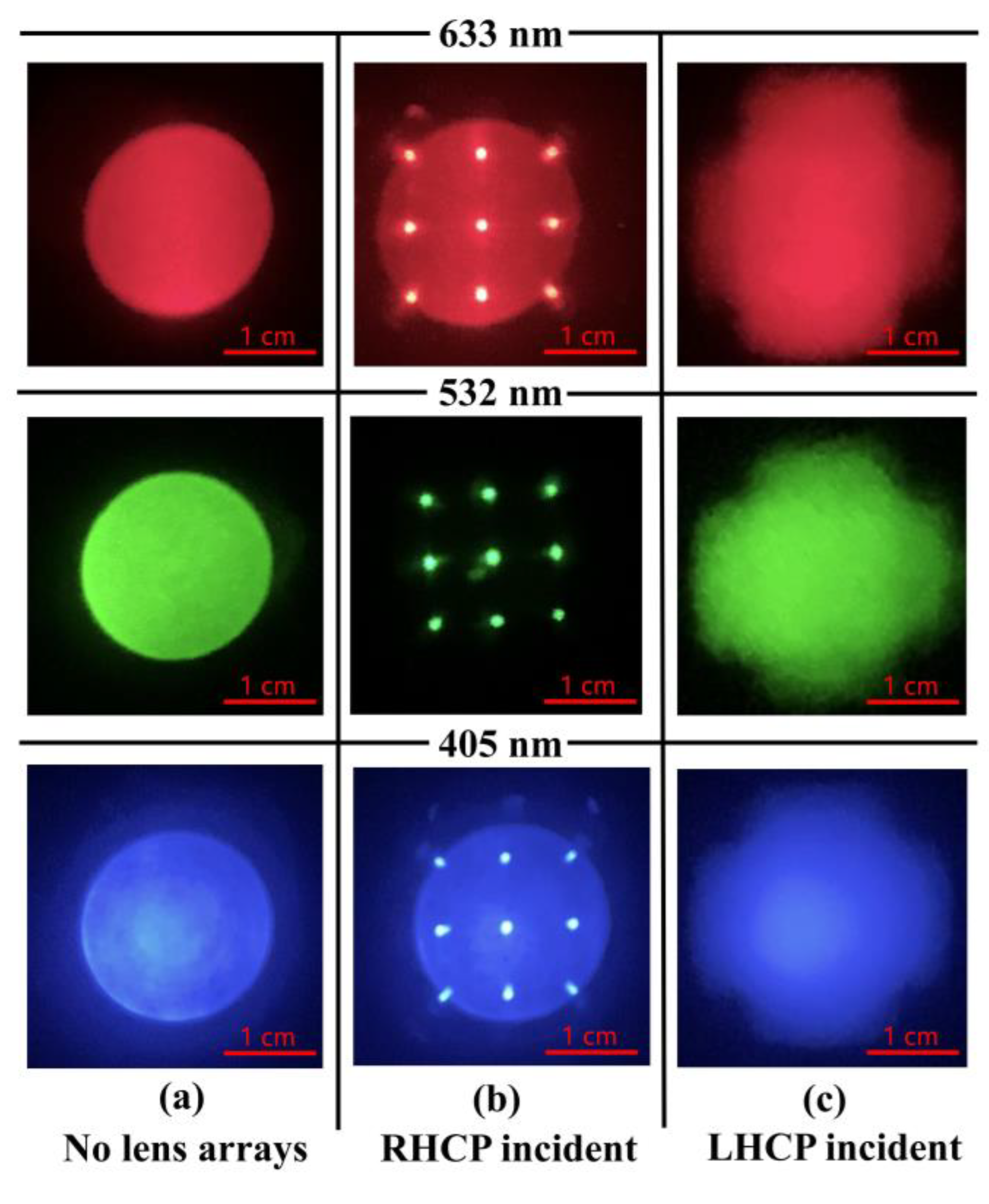
3. Results and Discussion

Here, we delve deeper into the intricacies of the molecular structure and imaging quality exhibited by the LCP. As evidenced in Figure 4a,b, the polarization microscope (POM) diagram of the LCP reveals distinct bright and dark rings. These rings undergo a phase change of 2π, corresponding to six discrete molecular orientations: 0°, 30°, 60°, 90°, 120°, and 150°. Notably, when the sample is rotated by 45°, the appearance of the rings reverses, while the vertically aligned LC region maintains consistent brightness under the POM. To assess the quality of the prepared lens, we conducted a detailed analysis of its morphological characteristics and splicing accuracy by examining the enlarged edges. The edge ring demonstrates a smooth morphology, with an edge line width measuring approximately 6.48 μm. This value deviates slightly from the theoretical design specification of 6.36 μm, resulting in a 1.9% error relative to the theoretical value. Notably, the observed splicing error is comparable to the size difference between the adjacent ring bands at the edge. Had the splicing error been significant, it would have been considerably larger than this size difference. Therefore, it can be confidently asserted that the splicing error is minimal, as further confirmed by Figure 4c,d. The dashed box area in Figure 4c represents the adjacent smooth texture zone, which is attributed to the self-smoothing properties of LC molecules. The solid box area in Figure 4d represents a single annular band of the LCP lens.
Utilizing the optical path illustrated in Figure 5a, we characterized the optical performance of the lens. The laser undergoes a series of transformations: passing through a beam expander and collimator, undergoing linear polarization enhancement via a polarizer, and being converted into circularly polarized light through a quarter-wave plate before incident on the lens sample. Subsequently, the focused spot is magnified tenfold by the lens and imaged on a CCD camera (Figure 5b). The Gaussian intensity profile of the focused spot indicates excellent imaging quality, as depicted in Figure 5c, showcasing a three-dimensional intensity distribution. Further analysis involves extracting intensity data along the vertical direction (we draw curves by sampling at regular intervals) and fitting it (represented by the X and Y axes in Figure 5d,e, respectively). The actual size of the focused spot in the X-axis and Y-axis directions measures 33.29 μm and 32.97 μm, respectively, representing an error of approximately 40% compared to their theoretical values (derived from the formula 1.22λ/NA = 23.2 μm). This suggests that the produced sample approaches the diffraction limit and exhibits excellent imaging performance. Figure 5f illustrates the focusing behavior of the lens at different positions.
As demonstrated in Figure 6a–c, the focusing capabilities of the lens sample were examined using laser light sources operating at 633 nm, 532 nm, and 405 nm wavelengths. The PB-phase LCP lens exhibits polarization-dependent behavior, converging right-handed circularly polarized (RHCP) light and diverging left-handed circularly polarized (LHCP) light. By rotating the quarter-wave plate, we could switch the polarization of the laser light from right-handed to left-handed circular polarization. In column a, the incident light is projected onto the screen without passing through the lens, providing a baseline for comparison. Column b showcases the effect of the RHCP light incident on the lens. In this configuration, the lens behaves like a convex lens with a positive focal length, effectively converging the light. Moving to column c, we observe the behavior of the lens when exposed to LHCP light. Here, the lens transforms into a concave lens with a negative focal length, causing the collimated incident beam to diverge. This polarization-dependent behavior is a unique characteristic of the PB-phase LCP lens. When observing the focusing spot, it is evident that the lens performs exceptionally well at the working wavelength of 633 nm, achieving a diffraction efficiency of 85.7%. Additionally, it also demonstrates good focusing capabilities for light sources in other wavelength bands.
We further fabricated a lens array, and the molecular structure diagram of an individual lens is depicted in Figure 7a–f. Figure 7a shows the POM image of the central area of the single LCP lens on the lens array. Figure 7b,c show the POM images of the edge area of the single LCP lens on the lens array, captured at 0° and 45° orientations. The dashed box area in Figure 7b represents the adjacent texture smooth zone, which is attributed to the self-smoothing characteristics of LC molecules. The solid box area in Figure 7c represents the single annular band of the LCP lens. Figure 7d–f show the POM images of the lens array at different positions. The measured edge linewidth is approximately 7.78 μm, differing by 160 nm from the theoretical design of 7.62 μm, representing a 2.1% error from the theoretical value. This level of splicing error closely matches the size difference between adjacent edge bands, indicating a very low splicing error. The splicing error is minimal, as a significant splicing error would surpass the size difference between adjacent edge bands. To characterize the optical performance of the lens array, we employed the same optical path described earlier (the difference is that the focusing spot does not need to be enlarged, and the data do not require interval sampling for curve drawing). Figure 8a displays the focusing spot image of the array captured by a CCD camera, while Figure 8b showcases the three-dimensional intensity distribution of the focusing spot of a single lens. Intensity data along the vertical direction were extracted and fitted, as represented by the X and Y axes in Figure 8c,d, respectively. The actual size of the focused spot in the X-axis and Y-axis directions measures 57.65 μm and 58.32 μm, respectively, with an error of approximately 30% compared to their respective theoretical values (45.6 μm). Furthermore, we utilized 633 nm, 532 nm, and 405 nm laser light sources to test the focusing performance of the lens array (Figure 9a–c). Column (a) represents the incident light on the screen without a lens array, column (b) represents the incident RHCP light, and column (c) represents the incident LHCP light. Observing the focusing spot, it becomes evident that the focusing effect of the lens array at the working wavelength (532 nm) is excellent, with an average diffraction efficiency of 83.3%. Additionally, it exhibits good focusing performance with light sources in other wavelength bands.

4. Conclusions

In conclusion, we propose a method for producing LC planar optical devices known as dynamic polarization patterning technology. Through precise control systems, we can generate real-time polarization patterning exposure while continuously moving the stitching process, thus eliminating the inertia-induced stoppage of the stitching step. This approach significantly reduces interface splicing errors compared to traditional polarization direct writing methods. As demonstrated by the fabrication of a lens and lens array, the splicing errors range from 100 nm to 200 nm, with an actual error of 1.9% to 2.1% compared to their theoretical values. This level of error is nearly on par with the difference in size between adjacent edge bands. If the splicing errors were significant, they would surpass the difference in size between adjacent edge bands; thus, our results indicate minimal splicing errors. Furthermore, optical path testing confirmed the excellent focusing effects of the produced lens and array. Our entire production process involves only coating a photo-alignment layer, polarization patterning, coating an LCP layer, and curing into a film, without the need for additional complex steps. This simplified approach holds promise for reducing the cost of industrialization.

Author Contributions

Conceptualization, W.H. and X.-j.Z.; methodology, X.Z., X.-j.Z., and X.Q.; software, X.Q. and K.Z.; validation, X.Q. and K.Z.; writing—original draft preparation, X.Q., W.H., and X.Z.; writing—review and editing, X.Q., W.H., and L.C.; supervision, W.H. and L.C. All authors have read and agreed to the published version of the manuscript.

Funding

National Key Research and Development Program of China (2022YFB3606603); National Natural Science Foundation of China (62175170, 62275180); Priority Academic Program Development of Jiangsu Higher Education Institutions.

Institutional Review Board Statement

Not applicable.

Informed Consent Statement

Not applicable.

Data Availability Statement

Data are contained within the article.

Conflicts of Interest

The authors declare no conflicts of interest.

References

  1. Komanduri, R.K.; Escuti, M.J. High efficiency reflective liquid crystal polarization gratings. Appl. Phys. Lett. 2009, 95, 091106. [Google Scholar] [CrossRef]
  2. Lin, T.; Xie, J.; Zhou, Y.; Zhou, Y.; Yuan, Y.; Fan, F.; Wen, S. Recent advances in photoalignment liquid crystal polarization gratings and their applications. Crystals 2021, 11, 900. [Google Scholar] [CrossRef]
  3. De Sio, L.; Tabiryan, N.; McConney, M.; Bunning, T.J. Cycloidal diffractive waveplates fabricated using a high-power diode-pumped solid-state laser operating at 532 nm. J. Opt. Soc. Am. B 2019, 36, D136–D139. [Google Scholar] [CrossRef]
  4. Tabiryan, N.V.; Serak, S.V.; Nersisyan, S.R.; Roberts, D.E.; Zeldovich, B.Y.; Steeves, D.M.; Kimball, B.R. Broadband waveplate lenses. Opt. Express 2016, 24, 7091–7102. [Google Scholar] [CrossRef] [PubMed]
  5. Serak, S.V.; Roberts, D.E.; Hwang, J.Y.; Nersisyan, S.R.; Tabiryan, N.V.; Bunning, T.J.; Steeves, D.M.; Kimball, B.R. Diffractive waveplate arrays. J. Opt. Soc. Am. B 2017, 34, B56–B63. [Google Scholar] [CrossRef]
  6. Yu, H.; Zhou, Z.; Qi, Y.; Zhang, X.; WEI, Q.H. Pancharatnam–Berry optical lenses. J. Opt. Soc. Am. B 2019, 36, D107–D111. [Google Scholar] [CrossRef]
  7. Feng, W.; Liu, Z.; Liu, H.; Ye, M. Design of tunable liquid crystal lenses with a parabolic phase profile. Crystals 2022, 13, 8. [Google Scholar] [CrossRef]
  8. Chen, P.; Ma, L.L.; Duan, W.; Chen, J.; Ge, S.J.; Zhu, Z.H.; Tang, M.J.; Xu, R.; Gao, W.; Li, T.; et al. Digitalizing self-assembled chiral superstructures for optical vortex processing. Adv. Mater. 2018, 30, 1705865. [Google Scholar] [CrossRef] [PubMed]
  9. Duan, W.; Chen, P.; Ge, S.J.; Wei, B.Y.; Hu, W.; Lu, Y.Q. Helicity-dependent forked vortex lens based on photo-patterned liquid crystals. Opt. Express 2017, 25, 14059–14064. [Google Scholar] [CrossRef] [PubMed]
  10. Chen, P.; Wei, B.Y.; Hu, W.; Lu, Y.Q. Liquid-Crystal-Mediated Geometric Phase: From Transmissive to Broadband Reflective Planar Optics. Adv. Mater. 2020, 32, 1903665. [Google Scholar] [CrossRef] [PubMed]
  11. Tabiryan, N.V.; Roberts, D.E.; Liao, Z.; Hwang, J.Y.; Moran, M.; Ouskova, O.; Pshenichnyi, A.; Sigley, J.; Tabirian, A.; Vergara, R.; et al. Advances in Transparent Planar Optics: Enabling Large Aperture, Ultrathin Lenses. Adv. Opt. Mater. 2021, 9, 2001692. [Google Scholar] [CrossRef]
  12. Li, S.; Liu, Y.; Li, Y.; Liu, S.; Chen, S.; Su, Y. Fast-response Pancharatnam-Berry phase optical elements based on polymer-stabilized liquid crystal. Opt. Express 2019, 27, 22522–22531. [Google Scholar] [CrossRef] [PubMed]
  13. De Sio, L.; Roberts, D.E.; Liao, Z.; Nersisyan, S.; Uskova, O.; Wickboldt, L.; Tabiryan, N.; Steeves, D.M.; Kimball, B.R. Digital polarization holography advancing geometrical phase optics. Opt. Express 2016, 24, 18297–18306. [Google Scholar] [CrossRef] [PubMed]
  14. Li, Y.; Zhan, T.; Wu, S.T. Flat cholesteric liquid crystal polymeric lens with low f-number. Opt. Express 2020, 28, 5875–5882. [Google Scholar] [CrossRef] [PubMed]
  15. Zhan, T.; Lee, Y.H.; Wu, S.T. High-resolution additive light field near-eye display by switchable Pancharatnam–Berry phase lenses. Opt. Express 2018, 26, 4863–4872. [Google Scholar] [CrossRef] [PubMed]
  16. Zhan, T.; Xiong, J.; Lee, Y.H.; Wu, S.T. Polarization-independent Pancharatnam-Berry phase lens system. Opt. Express 2018, 26, 35026–35033. [Google Scholar] [CrossRef] [PubMed]
  17. Yin, K.; Xiong, J.; He, Z.; Wu, S.T. Patterning liquid-crystal alignment for ultrathin flat optics. ACS Omega 2020, 5, 31485–31489. [Google Scholar] [CrossRef] [PubMed]
  18. Ying, J.; Zheng, J. Fingerprint sensor using a polymer dispersed liquid crystal holographic lens. Appl. Opt. 2010, 49, 4763–4766. [Google Scholar]
  19. Zhang, X.J.; Zhou, X.; Yang, Z.X.; Zhang, L.X.; Huang, W.; Chen, L. High-throughput and controllable manufacturing of liquid crystal polymer planar microlens array for compact fingerprint imaging. Opt. Express 2022, 30, 3101–3112. [Google Scholar] [CrossRef] [PubMed]
  20. Xiong, J.; Hsiang, E.L.; He, Z.; Zhan, T.; Wu, S.T. Augmented reality and virtual reality displays: Emerging technologies and future perspectives. Light. Sci Appl. 2021, 10, 216. [Google Scholar] [CrossRef] [PubMed]
  21. Yin, K.; Hsiang, E.L.; Zou, J.; Li, Y.; Yang, Z.; Yang, Q.; Lai, P.C.; Lin, C.L.; Wu, S.T. Advanced liquid crystal devices for augmented reality and virtual reality displays: Principles and applications. Light. Sci Appl. 2022, 11, 161. [Google Scholar] [CrossRef] [PubMed]
  22. Zhao, X.; Bermak, A.; Boussaid, F.; Chigrinov, V.G. Liquid-crystal micropolarimeter array for full Stokes polarization imaging in visible spectrum. Opt. Express 2010, 18, 17776–17787. [Google Scholar] [CrossRef] [PubMed]
  23. Yang, Z.X.; Shou, Q.L.; Zhou, X.; Zhang, X.J.; Huang, W.; Chen, L. Wide field of view chiral imaging with a liquid crystal planar lens enabled by digitalized nanogratings. Opt. Express 2022, 30, 44864–44877. [Google Scholar] [CrossRef] [PubMed]
  24. García de Blas, M.; Geday, M.A.; Otón, J.M.; Arregui, X.Q. Two-dimensional digital beam steering based on liquid crystal phase gratings. Appl. Sci. 2021, 11, 3632. [Google Scholar] [CrossRef]
  25. Gou, F.; Peng, F.; Ru, Q.; Lee, Y.H.; Chen, H.; He, Z.; Zhan, T.; Vodopyanov, K.L.; Wu, S.T. Mid-wave infrared beam steering based on high-efficiency liquid crystal diffractive waveplates. Opt. Express 2017, 25, 22404–22410. [Google Scholar] [CrossRef]
  26. Slussarenko, S.; Francescangeli, O.; Simoni, F. High resolution polarization gratings in liquid crystals. Appl. Phys. Lett. 1997, 71, 3613–3615. [Google Scholar] [CrossRef]
  27. Zhan, T.; Xiong, J.; Lee, Y.H.; Chen, R.; Wu, S.T. Fabrication of Pancharatnam-Berry phase optical elements with highly stable polarization holography. Opt. Express 2019, 27, 2632–2642. [Google Scholar] [CrossRef]
  28. He, Z.; Yin, K.; Wu, S.T. Standing wave polarization holography for realizing liquid crystal Pancharatnum-Berry phase lenses. Opt. Express 2020, 28, 21729–21736. [Google Scholar] [CrossRef] [PubMed]
  29. Presnyakov, V.; Asatryan, K.; Galstian, T.; Chigrinov, V. Optical polarization grating induced liquid crystal micro-structure using azo-dye command layer. Opt. Express 2006, 14, 10558–10564. [Google Scholar] [CrossRef] [PubMed]
  30. Wu, H.; Hu, W.; Hu, H.C.; Lin, X.W.; Zhu, G.; Choi, J.W.; Chigrinov, V.; Lu, Y.Q. Arbitrary photo-patterning in liquid crystal alignments using DMD based lithography system. Opt. Express 2012, 20, 16684–16689. [Google Scholar] [CrossRef]
  31. Duan, W.; Chen, P.; Ge, S.J.; Liang, X.; Hu, W. A fast-response and helicity-dependent lens enabled by micro-patterned dual-frequency liquid crystals. Crystals 2019, 9, 111. [Google Scholar] [CrossRef]
  32. Miskiewicz, M.N.; Escuti, M.J. Direct-writing of complex liquid crystal patterns. Opt. Express 2014, 22, 12691–12706. [Google Scholar] [CrossRef] [PubMed]
  33. Miskiewicz, M.N.; Escuti, M.J. Optimization of direct-write polarization gratings. Opt. Eng. 2015, 54, 025101. [Google Scholar] [CrossRef]
  34. Kim, J.; Li, Y.; Miskiewicz, M.N.; Oh, C.; Kudenov, M.W.; Escuti, M.J. Fabrication of ideal geometric-phase holograms with arbitrary wavefronts. Optica 2015, 2, 958–964. [Google Scholar] [CrossRef]
  35. Meng, Z.; Huang, W.; Zhang, L.X.; Zhou, X.; Zhao, K.; Pu, D.; Chen, L. Large aperture and defect-free liquid crystal planar optics enabled by high-throughput pulsed polarization patterning. Opt. Express 2023, 31, 30435–30445. [Google Scholar] [CrossRef] [PubMed]
  36. Miyamoto, K. The phase Fresnel lens. J. Opt. Soc. Am. 1961, 51, 17–20. [Google Scholar] [CrossRef]
  37. Honma, M.; Nose, T. Liquid-crystal Fresnel zone plate fabricated by microrubbing. Jpn. J. Appl. Phys. 2005, 44, 287. [Google Scholar] [CrossRef]
  38. Xu, Q.; Sun, T.; Wang, C. Coded liquid crystal metasurface for achromatic imaging in the broadband wavelength range. ACS Appl. Nano. Mater. 2021, 4, 5068–5075. [Google Scholar] [CrossRef]
Figure 1. Schematic illustration of dynamic polarization patterning technology. (a) Machine working route. (b) System patterning process.
Photonics 11 00350 g001
Figure 2. Schematic illustration of dynamic polarization patterning technology system optical path.
Photonics 11 00350 g002
Figure 3. Fabrication of the LCP lens and the LCP lens array using the dynamic polarization patterning technology. (a) Dropwise addition of the photo-alignment agent; (b) spin coating the photo-alignment layer; (c) dynamic polarization pattering using the system to orient the photo-alignment layer; (d) dropwise addition of the LCP solution; (e) spin coating the LCP solution; (f) UV curing the LCP to stabilize the molecular orientation.
Photonics 11 00350 g003
Figure 4. Characterization of the LCP lens. (a,b) POM images of the central area of the LCP lens, captured at 0° and 45° orientations. (c,d) POM images of the edge area of the LCP lens, captured at 0° and 45° orientations.
Photonics 11 00350 g004
Figure 5. Optical characterization of the LCP lens. (a) Schematic illustration of the optical path for testing the lens focusing performance. (b) Focus image captured by CCD. (c) Three-dimensional intensity profile of the focused spot. (d,e) Intensity distribution of the focused spot at different di− rections. (f) Schematic illustration of the lens focusing captured by CCD at different distances.
Photonics 11 00350 g005
Figure 6. Focused images of the LCP lens using 633 nm, 532 nm, and 405 nm laser beams. (a) No lenses. (b) Using RHCP light for incidence. (c) Using LHCP light for incidence.
Photonics 11 00350 g006
Figure 7. Characterization of the LCP lens array. (a) POM image of the central area of the single LCP lens on the lens array. (b,c) POM images of the edge area of the single LCP lens on the lens array, captured at 0° and 45° orientations. (df) POM images of different locations in the array.
Photonics 11 00350 g007
Figure 8. Optical characterization of the LCP lens array. (a) Focus images captured by CCD. (b) The 3D intensity profile of the focused spot of a single LCP lens on the lens array. (c,d) Intensity distri− bution of the focused spot at different directions.
Photonics 11 00350 g008
Figure 9. Focused images of the LCP lens array using 633 nm, 532 nm, and 405 nm laser beams. (a) No lens arrays. (b) Using RHCP light for incidence. (c) Using LHCP light for incidence.
Photonics 11 00350 g009
Disclaimer/Publisher’s Note: The statements, opinions and data contained in all publications are solely those of the individual author(s) and contributor(s) and not of MDPI and/or the editor(s). MDPI and/or the editor(s) disclaim responsibility for any injury to people or property resulting from any ideas, methods, instructions or products referred to in the content.

