1. Introduction
In optical absorbers, Al
2O
3 and SiO
2 are frequently utilized as thin-film dielectric materials. They offer several advantages, notably exceptional transparency across a broad spectrum of wavelengths, with particular emphasis on their high transparency within the visible light range. Moreover, they demonstrate impressive thermal stability and robust chemical resilience, enabling them to withstand various oxidation processes and chemical corrosions. This renders them highly reliable in diverse environmental conditions. Additionally, their manufacturing processes are well-established, allowing for the production of materials in various forms and sizes such as thin films, nanoparticles, and nanowires. Their optical properties are easily tunable, enabling precise control over parameters such as structure and thickness to manipulate optical behaviors, including absorption, scattering, and transmission of light. These attributes make Al
2O
3 and SiO
2 ideal choices for numerous optical applications [
1,
2,
3,
4]. Titanium (Ti) is frequently utilized in the manufacturing processes of optical absorbers because of its exceptional absorption characteristics in the visible light and near-infrared spectra. This attribute enables efficient absorption of light energy within these wavelength ranges, making it an excellent choice for achieving high absorption efficiency within such spectra. Moreover, the optical properties of Ti can be fine-tuned by adjusting various factors in the manufacturing process, allowing for the optimization of Ti’s absorption characteristics to meet the specific design requirements of various optical absorbers.
Additionally, Ti offers good corrosion resistance, benefits from relatively mature manufacturing processes, and is more cost-effective compared to certain other high-performance optical metals. Consequently, Ti finds widespread utilization in the production of optical absorbers [
5,
6,
7]. Designing an optical absorber that achieves high absorption efficiency across the near-ultraviolet, visible, and mid-infrared spectra presents a challenging problem. This is because light of different wavelengths interacts with materials in diverse ways, and materials themselves exhibit varying absorption characteristics across different wavelengths. In past optical absorber designs, balancing different factors has typically been necessary to achieve high absorptivity across multiple wavelength ranges. Several effective strategies exist for optimizing light absorption across various wavelength ranges. These strategies include utilizing multilayered structures to allow for fine-tuning absorption efficiency across different wavelengths [
8], employing nanoscale structures and surface modifications to provide control over absorption efficiency for specific wavelengths [
9], selecting materials with broad wavelength absorption characteristics and adjusting their structure and composition through synthesis methods to facilitate achieving high absorption rates across multiple wavelength ranges [
10], and implementing optical resonance structures to enhance absorption within targeted wavelength ranges [
11].
In the realm of optical engineering, crafting an absorber capable of achieving exceptional absorption rates across a broad spectrum of wavelengths demands meticulous attention to various factors, including material properties, structural design, and optical characteristics. This endeavor often entails intricate multi-level optimization and fine-tuning. Over time, researchers have explored diverse structural designs in the quest for absorbers exhibiting high absorption efficiency over an extensive range of wavelengths. Among the array of approaches, two predominant strategies have emerged as particularly promising: microstructure arrays and multilayered structures. Microstructure arrays involve the fabrication of micron-scale patterns, such as nanoholes or pillar structures, offering tailored absorption capabilities within the ultra-wide band spectrum. These intricate structures can be precisely engineered to target specific wavelengths of light, providing flexibility and customization to meet diverse application [
12] requirements. Conversely, multilayered structures involve the strategic stacking of layers comprising different materials arranged in specific configurations. Each layer is meticulously designed to absorb light within a designated wavelength range, resulting in remarkable absorption performance spanning the entire spectrum [
13,
14]. Through extensive explorations and analyses, researchers can continue to refine and optimize these approaches, pushing the boundaries of absorption efficiency and opening new avenues for applications in fields ranging from photovoltaics to optical sensing.
Metamaterials find applications across various fields and functionalities. For instance, Liang et al. explored an innovative thermal radiation emitter with intelligent temperature control, utilizing a layered structure comprising the phase change material VO
2 [
15]. Additionally, Yue et al. introduced a pioneering approach that combines metasurfaces and Fresnel zone plates to create a metasurface zone plate. This design facilitates the conversion of nearly arbitrary polarizations into a fixed polarization [
16]. Metasurfaces, possessing extraordinary capabilities for manipulating electromagnetic (EM) waves, have led to the development of a wide range of advanced metadevices with fascinating functionalities. For instance, Zeng et al. successfully utilized graphene as a promising candidate to enhance metasurfaces, enabling remarkably dynamic tenability [
17]. The pyramid-like absorber, designed with gradually decreasing square side lengths from bottom to top, is a common structure known as a pyramid structure. In previous work, Li et al. had introduced a groundbreaking concept: a polarization-independent tunable bandwidth absorber utilizing a monolayer graphene. This innovative design boasts the capability of achieving an absorptivity surpassing 0.9 within the 3–6 THz band. This significant advancement not only underscores the versatility and potential of graphene-based technologies [
18]. Cui et al. introduced an absorber employing a sawtooth anisotropic metamaterial. This absorber features a nanostructure comprising 20 pairs of alternating flat layers of gold and germanium plates, with gradually increasing cross-sections atop a gold substrate. However, the absorption efficiency of this absorber exceeded 90% within a wavelength range of approximately 2.9 μm to 5.75 μm [
19]. Wang and Cheng employed Bi
2Te
3 deposited on a silver substrate, ranging in thickness from tens to hundreds of nanometers, to propose a square pyramidal nanostructure absorber for solar energy harvesting [
20].
The proposed periodic pyramidal nanostructures had a height of 3000 nm, with the upper square side measuring 4 nm and the bottom square side measuring 200 nm. While this absorber exhibited a broad absorption bandwidth with efficiency surpassing 0.900 (90%), it still fell short of achieving efficiencies exceeding 0.900 simultaneously across the ultraviolet and mid-infrared spectrum. Additionally, this structure posed challenges in terms of manufacturing. The main drawback is that fabricating pyramid structures with precise dimensions and stacking arrangements may require complex processing techniques, thus increasing manufacturing costs and difficulty. The structure in our study resembles a pyramid, consisting of four square layers with different side lengths stacked on top of each other. Each square is composed of a layer of metal and oxide structures. The square sides gradually decrease in length from the bottom to the top, avoiding the complex structures of tetrahedral or pentahedral pyramids that are difficult to fabricate. The advantages of this design include:
- (1)
Broadband absorption characteristics: Pyramid structures can achieve light absorption across a wide spectrum range because pyramids of varying sizes induce resonance effects at different frequencies.
- (2)
Low reflectance: This structure effectively reduces light reflection as incident light undergoes multiple reflections at different layers, thereby increasing the chances of light absorption.
- (3)
Multilayered design for adjustable absorption spectrum: By designing pyramid structures of different sizes and stacking arrangements, the characteristics of the absorption spectrum can be adjusted to meet the specific requirements of various applications.
- (4)
Increased optical path: Multilayered pyramid structures increase the path length of light propagation within the absorber, contributing to enhanced absorption efficiency.
Our distinguishing feature lies in the simplicity of the structure compared to many traditional pyramids in the past. This design choice offers several advantages. Firstly, the simpler structure facilitates fabrication, reducing production costs and time. Secondly, it allows for easier analysis and understanding of the material properties and behaviors within the pyramid structure. Additionally, the gradual decrease in square size from the base to the top potentially enables interesting variations in material characteristics or functionalities along the vertical axis. Moreover, the pyramid-like configuration inherently provides stability and strength, making it suitable for various applications in material science, architecture, or even nanoengineering. By leveraging this simplicity, we aim to explore novel properties and applications of materials within this unique geometric arrangement. Through experimental observation and theoretical analysis, we anticipate uncovering valuable insights that could contribute to advancements in various fields. However, in this study, the pyramid structure features decreasing side lengths from bottom to top, with a minimum thickness of Ti metal designed to be at least 50 nm, and only Al2O3, SiO2, and Ti materials are utilized. With modern semiconductor fabrication processes, manufacturing this structure should pose no significant challenges. More significantly, our design achieves a broadband absorber with a non-width-to-length ratio exceeding 0.900, spanning from ultraviolet A (335 nm) to middle infrared (4865 nm). This remarkable performance is a rarity in the field, as achieving such wide absorption efficiency with a simple optical absorber design has been exceedingly uncommon in the past.
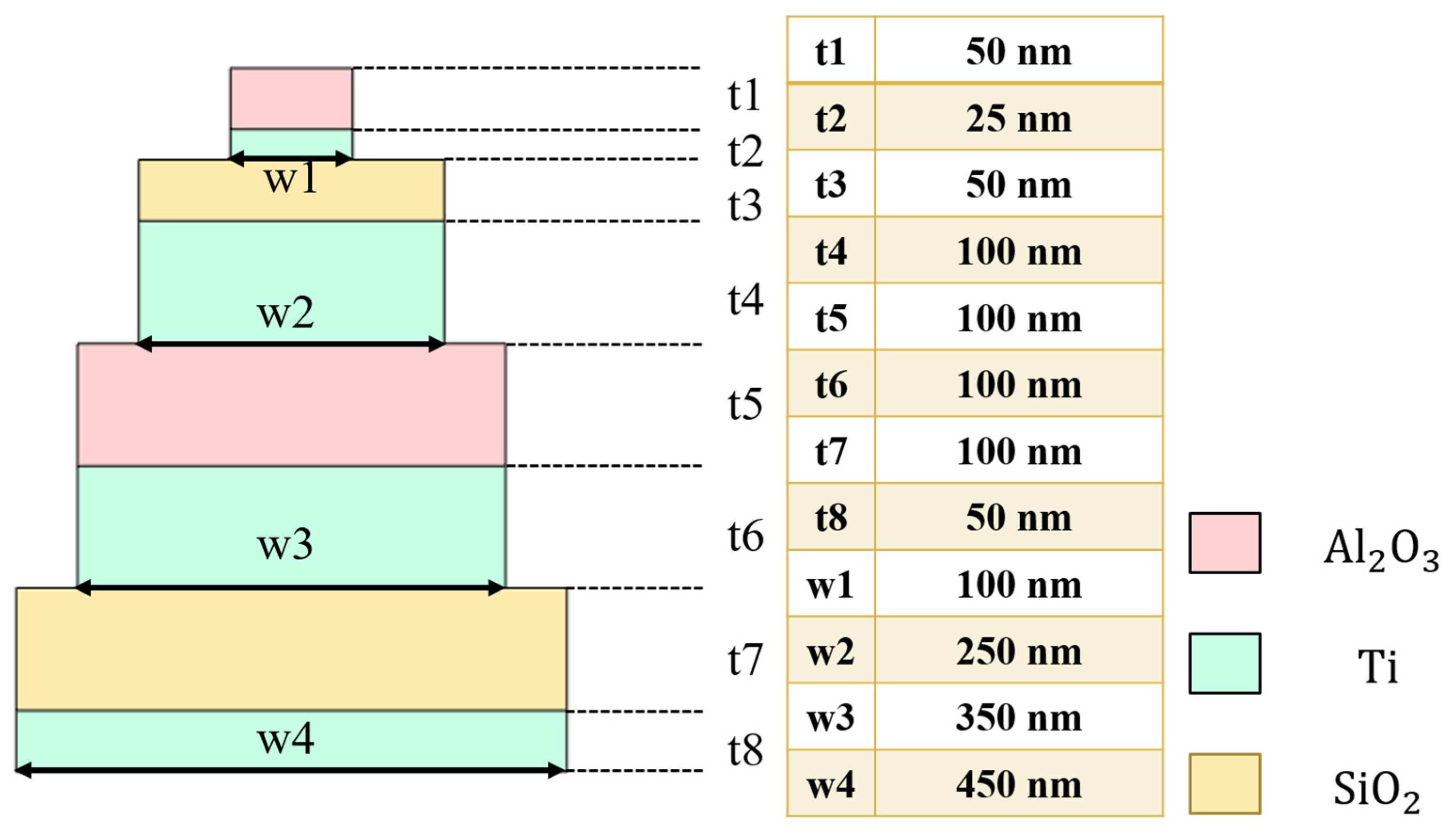
3. Results and Discussion
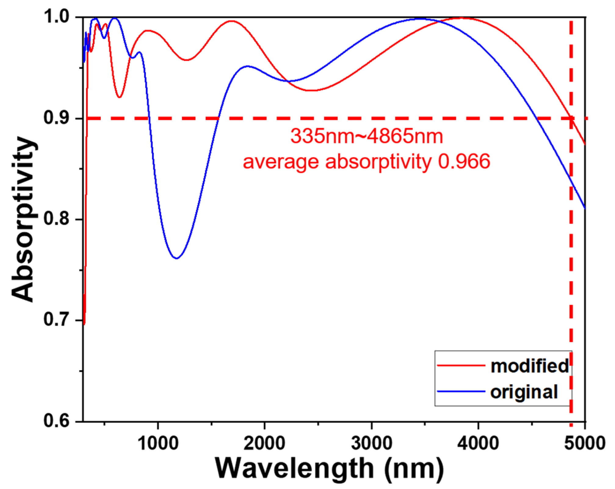
The simulation result using the parameters from
Figure 1 is presented in
Figure 2. As shown in
Figure 2, the spectrum from the original structure simulation (depicted by the blue line) clearly indicates that the absorptivity was below 0.900 within the range of 920–1565 nm, and it also dropped below 0.900 when the wavelength exceeded 4540 nm. While utilizing multilayered structures offers the potential for optimizing light absorptivity across various wavelength ranges, achieving high absorptivity across an ultra-wideband spectrum requires careful consideration and adjustment of each structural parameter. Hence, it is necessary to explore the optimal values for each parameter, including the thicknesses of t7-t1 layers and the widths of w4-w1. Each layer can be tailored to enhance absorption characteristics within specific wavelength ranges, thereby achieving high absorption rates across the entire spectrum. The adjustment of geometric parameters and optical properties of the structures enables selective absorption within desired wavelength ranges.
It is noteworthy that the t8 and t7 layers formed continuous planes, with the functions of adjustments to the width of w4 primarily regulating the spacings between adjacent t6-t1 layers. For instance, when w4 measured 450 nm and w3, w2, and w1 were 350 nm, 250 nm, and 100 nm, respectively, the spacings between adjacent t6-t5 layers, t4-t3 layers, and t2-t1 layers were 100 nm, 200 nm, and 250 nm. If w4 were to be adjusted to 490 nm while maintaining w3, w2, and w1 at 350 nm, 250 nm, and 100 nm, the spacings between adjacent t6-t5 layers, t4-t3 layers, and t2-t1 layers would increase to 140 nm, 240 nm, and 290 nm, respectively.
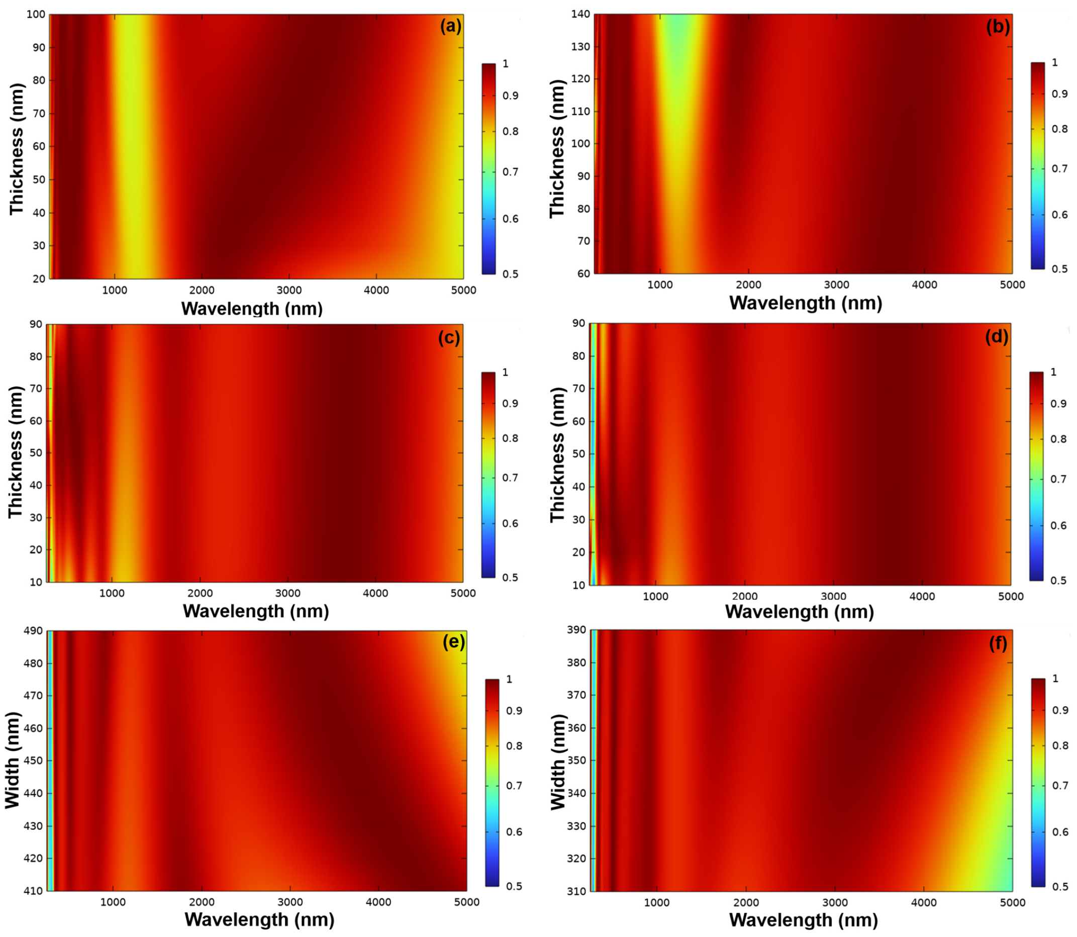
Figure 3a–f depict the variations in absorptivity observed in the examined pyramid-like absorber, stemming solely from adjustments in specific parameters: the thicknesses of layers t7-t1 and the widths of w4-w1. This evaluation centers on the pyramid-like absorber illustrated in
Figure 1.
Figure 3a highlights the impact on absorptivity when solely adjusting the thickness of the t7 layer within the range of 20 to 100 nm. As illustrated in
Figure 3a, enlarging the thickness of the t7 layer from 20 to 100 nm shifted the range where absorptivity was below 0.900 from approximately 1000–1550 nm to about 1000–1380 nm. Despite these adjustments, absorptivity remained below 90%, prompting the selection of a 100 nm thickness for the t7 layer. Specifically, with a t7 layer thickness of 100 nm, the examined pyramid-like absorber exhibited notable absorptivity within the wavelength ranges of 200–1000 nm and 1380–4850 nm.
The absorption characteristics of the investigated pyramid-like absorber for the t6 layer mirror those of the t7 layer and are not detailed separately here. As the thickness of the t6 layer ranged from 60 to 140 nm, the regions where absorptivity exceeded 0.900 shifted from approximately 300–920 nm and 1450–4500 nm to 300–1020 nm and 1380–5000 nm. Despite these modifications, absorptivity remained below 90% in certain ranges, leading to the choice of a 130 nm thickness for the t6 layer. Therefore, we continued to adjust other parameters. Continuing with the optimization simulations for the thickness variation of the t5 layer, the results are depicted in
Figure 3c. As shown in
Figure 3c, the variation in the thickness of the t5 layer leads to a contrary effect on the ranges where absorptivity falls below 0.900 compared to the t7 and t6 layers. When varying the thickness of the t5 layer from 60 to 140 nm, the ranges where absorptivity exceeded 0.900 shifted from approximately 300–1150 nm and 1420–5000 nm to 300–900 nm and 1550–5000 nm. This indicates that as the thickness of the t5 layer decreases, the range where absorptivity falls below 0.900 also decreases. However, despite the varying thicknesses of the t5 layer, absorptivity remained below 90% in certain ranges. Therefore, we determined 80 nm as the optimal thickness for the t5 layer.
The influence of the thickness of the T4 layer paralleled that of the T5 layer, and the simulation results are not illustrated here. When the thickness of the T4 layer varied from 60 to 140 nm, the spectral regions where absorptivity exceeded 0.900 shifted from approximately 350–1050 nm and 1150–4900 nm to 330–1100 nm and 1500–5000 nm. Clearly, through adjustments to the T4 layer, the absorptivity range of this investigated pyramid-like absorber nearly encompasses wavelengths from ultraviolet A to middle infrared. The chosen thickness of the T4 layer was 80 nm, primarily because at this thickness, wavelengths beyond 0.900 in the ultraviolet range could be blue-shifted to around 330 nm.
Figure 3c,d illustrate the absorptivity variations observed in the investigated absorber, which stem solely from adjustments in the thicknesses of the t3 and t2 layers. Notably, these figures depict absorptivity results corresponding to thicknesses of 10 nm and 90 nm. By choosing thicknesses of 70 nm and 50 nm for the t3 and t2 layers, respectively, our aim was to augment absorptivity specifically at the 1200 nm wavelength, without markedly compromising absorptivity within the sub-1000 nm range. This strategic selection enables the optimization of absorption efficiency at the targeted wavelength while preserving acceptable performance across neighboring wavelengths.
Moreover, opting for a 50 nm thickness for the t1 layer was grounded in its capability to maintain absorptivity at both 1200 nm and 2300 nm wavelengths. Furthermore, this thickness guarantees that absorptivity remains above 0.900 for wavelengths in the range of 335–400 nm. This multilayer configuration not only maximizes absorptivity at specific wavelengths of interest but also ensures satisfactory performance across a wider spectrum, rendering it suitable for diverse applications. Continuing with a further analysis of the influence of w4 and w3 on the entire absorption spectrum: as shown in
Figure 3e, when the value of w4 is set at 410 nm, it is evident that there are distinct troughs in absorptivity around 1200 nm and 2400 nm, respectively. However, when the width of w4 increases from 410 nm to 490 nm, although the long-wavelength positions where absorptivity exceeds 0.900 shift from around 5000 nm to approximately 4750 nm, the low absorptivity at 1200 nm and 2400 nm is improved to exceed 0.900. Additionally, perfect absorption with a value of 0.990 appears at 505 nm, 1690 nm, and 3840 nm. This scenario aligns with the optimal parameter absorption spectrum depicted in
Figure 2.
Furthermore, as illustrated in
Figure 3f, as the width of w3 expands from 310 nm to 390 nm, it becomes evident that the bandwidth of the absorption spectrum widens with the width of w3, and absorptivity in certain spectral bands also significantly increases. Consequently, widths of 490 nm and 390 nm are selected for w4 and w3, respectively. These observations indicate that adjusting the widths of w4 and w3 can significantly impact the absorption characteristics of the material, allowing for the optimization of absorptivity across different wavelengths. This understanding is pivotal for customizing the material’s properties to suit specific applications where absorption at particular wavelengths is imperative. When the square dimensions gradually diminish from bottom to top, several factors may contribute to a reduction in the absorptivity of the light absorber:
- (1)
Reflection and interference of light between different layers in the multilayer structure may cause some rays to be reflected rather than absorbed.
- (2)
As the square dimensions diminish, the propagation path of light between layers may lengthen, increasing the chances of light scattering or loss.
- (3)
When the square dimensions shrink to specific sizes, resonance effects between the wavelength and structural dimensions may occur, resulting in the capture or reflection of spectral energy at particular wavelengths.
These effects collectively contribute to the observed decrease in absorptivity in the optical absorber. Understanding these mechanisms is crucial for optimizing the design and performance of such absorbers across various applications. Factors that may contribute to an increase in the absorptivity of the optical absorber include:
- (1)
Adjusting the stacking order of the squares or altering the material composition of the squares may modify the propagation and absorption characteristics of light within the structure, thereby increasing absorptivity.
- (2)
Modifying the arrangement of squares or structural parameters, such as increasing the number of layers or adjusting the spacing between layers, can enhance the chances of light capture or absorption within the structure.
- (3)
Optimizing structural design, such as selecting specific thicknesses or material combinations, can improve the structure’s absorption efficiency for particular wavelengths of light.
In conclusion, the absorptivity of the investigated optical absorber is influenced by factors such as structural design and material selection. Through adjustments to these factors, it becomes feasible to effectively control variations in absorptivity. Likewise, the widths of w2 and w1 were fine-tuned from 200 to 290 nm and from 60 to 140 nm, respectively. Following comprehensive optimization, widths of 240 nm and 140 nm were chosen for w2 and w1, respectively. A comparison between the original design and the modified parameters is presented in
Table 1. Significantly, our designed pyramid-like absorber demonstrated absorptivity levels surpassing 90% across the wavelength range of 335 to 4865 nm under these specific parameters, as depicted by the red line in
Figure 2.
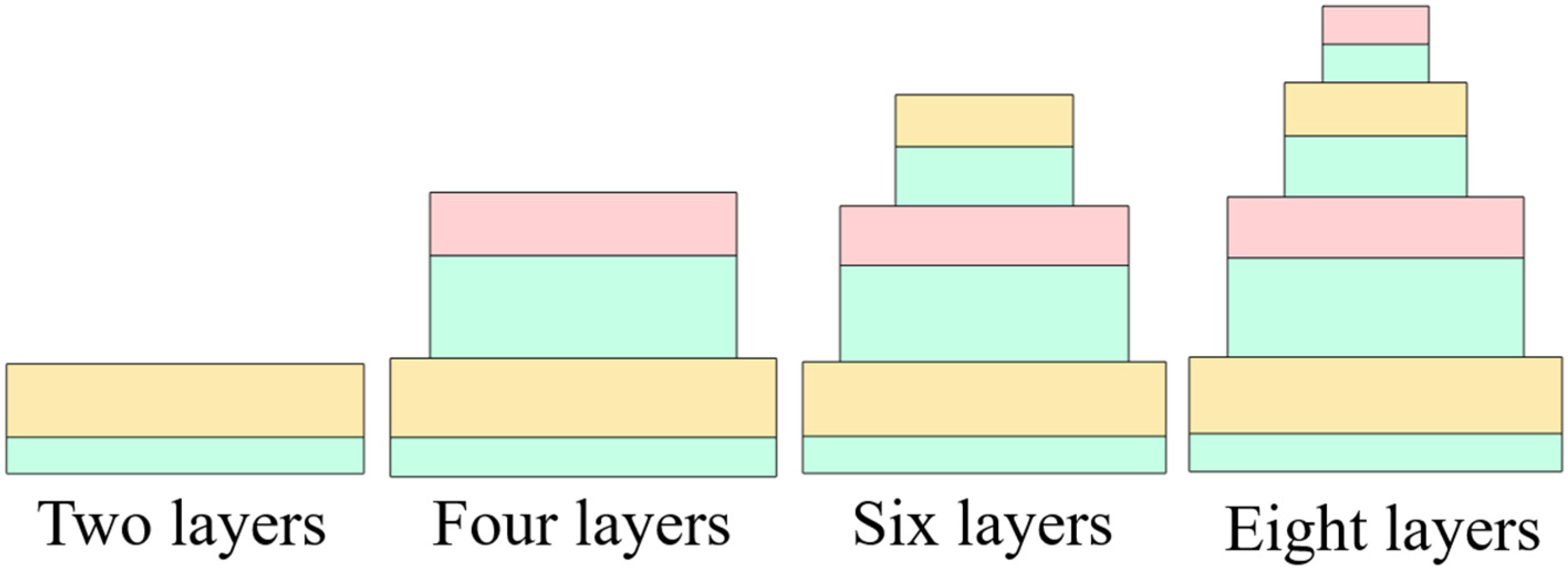
To grasp the principle behind the ultra-wideband support from ultraviolet A to middle infrared in this study, a series of analyses were conducted. The proposed structure of the optical absorber comprised a layer of square metal stacked atop a layer of square oxide, organized into four groups from bottom to top, with decreasing square side lengths. Initially, the absorption spectra for different numbers of groups were analyzed, including configurations with only t7-t8 layers, t5-t8 layers, t3-t8 layers, and t1-t8 layers. The values of w4, w3, w2, and w1 were maintained at 490 nm, 390 nm, 240 nm, and 140 nm, respectively, as illustrated in
Figure 4. In this structure, the optical absorber is induced by surface plasmon resonance. As shown in
Figure 5, when only t7-t8 layers are present, there is a single absorption peak at approximately 0.700 at 685 nm. However, with the structure changing to t5-t8 layers, a distinct absorption peak emerges at 3720 nm, also observed in the t3-t8 and t1-t8 layer structures. The emergence of lower wavelength absorption peaks between larger and smaller areas may be attributed to multimode resonance. In multimode resonance, a system can simultaneously support multiple resonance modes occurring at different wavelengths.
Typically, larger structures may support a greater number of resonance modes, which can lead to absorption peaks at lower wavelengths. This phenomenon arises from the complex interplay of electromagnetic fields within the structure, resulting in resonances at various wavelengths. Consequently, the spectral response of the system can exhibit distinct absorption features corresponding to these resonance modes. Furthermore, when the structure transitions to the t3-t8 layer mode, more absorption peaks at shorter wavelengths emerge, and these peaks also appear in the t1-t8 layer structure. In this proposed structure, the alternating arrangement of metal and oxide layers creates a resonance mode known as surface plasmon resonance, which leads to the absorption of photons and their conversion into energy. As the side length of the squares decreases, there is an increase in resonance frequency and a corresponding decrease in wavelength due to surface plasmon resonance. With different groups having decreasing square side lengths, the resonance effect at shorter wavelengths intensifies. The varying sizes of the different groups lead to corresponding changes in resonant wavelengths, further enhancing the absorption efficiency.
Surface plasmon resonance arises from the interface structure between metal and dielectric materials. When free electrons on the surface of a metal interact with light waves, collective oscillations called plasmons are generated. These plasmons result in enhanced absorption and scattering of light at specific wavelengths, a phenomenon known as surface plasmon resonance. Therefore, surface plasmon resonance is actually a phenomenon generated by the interface structure between metal and dielectric materials, rather than solely by the metal or dielectric material itself. Surface plasmon resonance is indeed correlated with the area it is generated in. Generally, for a given metal–dielectric interface structure, when the area is smaller, the resonance frequency (or wavelength) of surface plasmon resonance tends to be higher. This is because the localized effect of plasmon oscillations is more pronounced on smaller areas, resulting in higher resonance frequencies. Thus, it can be concluded that smaller areas generally result in higher resonance frequencies and shorter corresponding wavelengths for surface plasmon resonance. This relationship holds significant importance in the design and control of surface plasmon resonance, particularly in applications at the nanoscale and microstructures.
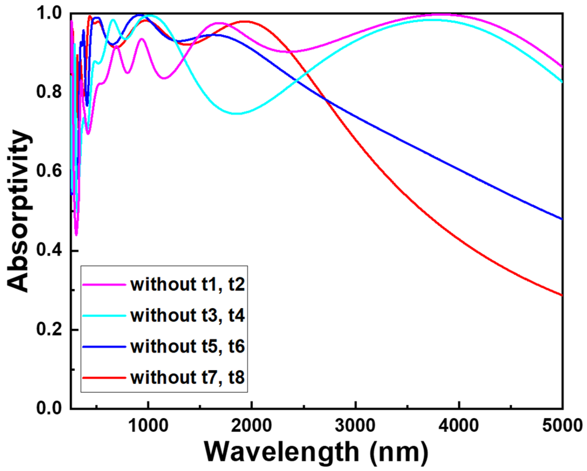
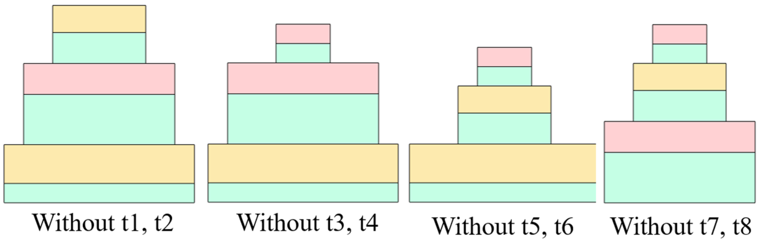
To further analyze the high absorptivity achieved by the structure in this study across an ultra-wideband from ultraviolet A (335 nm) to middle infrared (4865 nm), we kept the dimensions of w4, w3, w2, and w1 consistent at 490 nm, 390 nm, 240 nm, and 140 nm, respectively. However, we selectively removed different combinations of metal and oxide layers from t8-t1 layers. Specifically, we removed either t2-t1 layers, t4-t3 layers, t6-t5 layers, or t8-t7 layers, as
Figure 6 shows, and the simulation results are shown in
Figure 7. In our earlier analyses, it was observed that when the structure transitions to t5-t8 layers, a distinct absorption peak emerges at 3720 nm. However, in this analysis, we found that the absorption peak at 3720 nm disappears when either t8-t7 layers or t6-t5 layers are absent. This clearly indicates that the absorption peak at 3720 nm is attributed to the combined presence of t8-t5 layers rather than solely to t6-t5 layers alone. For optical absorbers, surface plasmon resonance is a common resonance phenomenon. In addition, interference effects can manifest in various ways within optical absorbers. Firstly, interference effects can either enhance or diminish light absorption, contingent on factors such as the wavelength of light, characteristics of the light source, and the structure of the absorber. Enhanced absorption peaks or absorption dips occur when light waves within the absorber interfere with their own reflections or with other light waves.
This interference effect can be managed by adjusting the structure or materials of the absorber, thereby achieving enhancement or suppression of light absorption within specific wavelength ranges. Precise design of the absorber’s structure enables selective absorption or reflection of light across different wavelength ranges, making it suitable for applications such as optical filters and solar cells. Additionally, the results from
Figure 7 clearly demonstrate that the removal of t2-t1 layers leads to a significant decrease in absorptivity for wavelengths below 1500 nm. Similarly, the removal of t4-t3 layers results in a noticeable decrease in absorptivity within the 1700–2800 nm wavelength range. Moreover, the spectra from removing t8-t7 layers show lower absorption at longer wavelengths compared to removing t6-t5 layers. These findings further corroborate that achieving broadband absorption involves not only surface plasmon resonance but also interference effects. In essence, the optimal parameter structure identified in this study, encompassing the thicknesses of t8-t1 layers and the widths of w4-w1, not only attains optimal surface plasmon resonance absorption characteristics but also amplifies interference effects to attain high absorptivity across the ultra-wideband spectrum of 335 nm to 4865 nm.
Oxides are commonly known as insulators or semiconductors, and their electronic structure differs from metals. Consequently, they lack the free electrons necessary to support the phenomenon of localized surface plasmon resonance. However, certain complex nanostructures may consist of a composite system containing both metals and oxides. In such instances, the localized surface plasmon resonance effect may manifest in the metallic portion while being absent in the oxide portion. Therefore, the topmost layer of oxides usually does not exhibit localized surface plasmon resonance effects, and the disappearance of the top oxide layer is likely attributed to other factors.
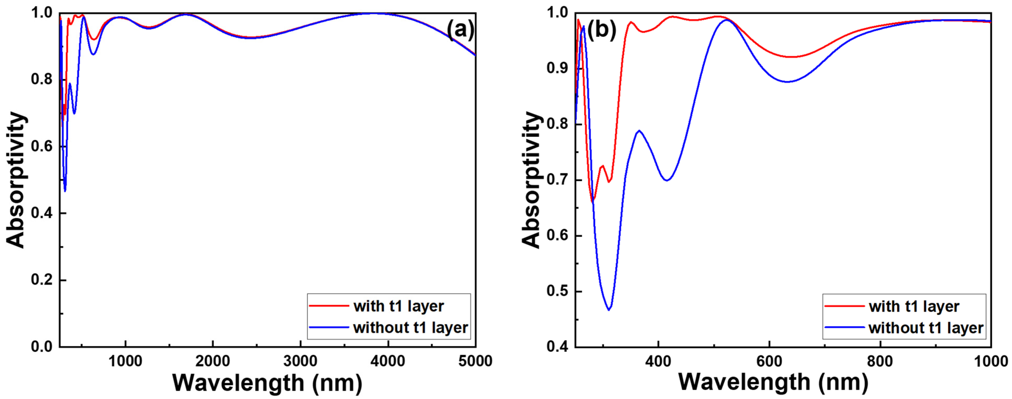
Figure 8 illustrates a comparison of absorption spectra with and without the t1 layer.
Figure 8a depicts an ultra-wideband spectrum ranging from 300 to 5000 nm, while
Figure 8b presents a narrowband spectrum spanning from 300 to 1000 nm. As shown in
Figure 8a, the absorption spectra of both configurations almost overlap when the wavelength exceeds 820 nm. In contrast,
Figure 8b demonstrates that for wavelengths shorter than 820 nm, the absorptivity of the configuration with the t1 layer is significantly higher than that without. Typically, the topmost layer of oxides functions as an anti-reflection coating (ARC) [
21,
22]. However, there is not a direct correlation between the size of the ARC layer and the anti-reflective wavelength. ARC layer design is typically optimized for specific wavelength ranges to minimize light reflection. This optimization takes into account factors such as incident angles of light and refractive indices of the medium.
Surface plasmon resonance wavelength is influenced by various factors, including the geometric shape of the metal surface, properties of the metal material, refractive index of the medium, and structural features of the resonant device. Typically, the resonance wavelength varies due to the interplay of these factors. For a given resonant device, tuning of the resonance wavelength is typically achieved by altering its size and geometry. Thus, when the oxide layer is removed, surface plasmon resonance may be affected and may not sustain. This is because the oxide layer not only serves as an interface between the medium and the metal surface but also influences the propagation of light in this system, thereby affecting the formation of plasmonic resonance. The presence of the oxide layer can modulate the coupling effects between light and the metal interface, influencing the frequency and intensity of surface plasmon resonance. Therefore, removing the oxide alters the optical properties of the interface, potentially leading to the disappearance or weakening of plasmonic resonance. Hence, in this study, the primary resonance effect is surface plasmon resonance, where different square shapes produce different resonance wavelengths, forming an ultra-wideband absorber structure in this research.
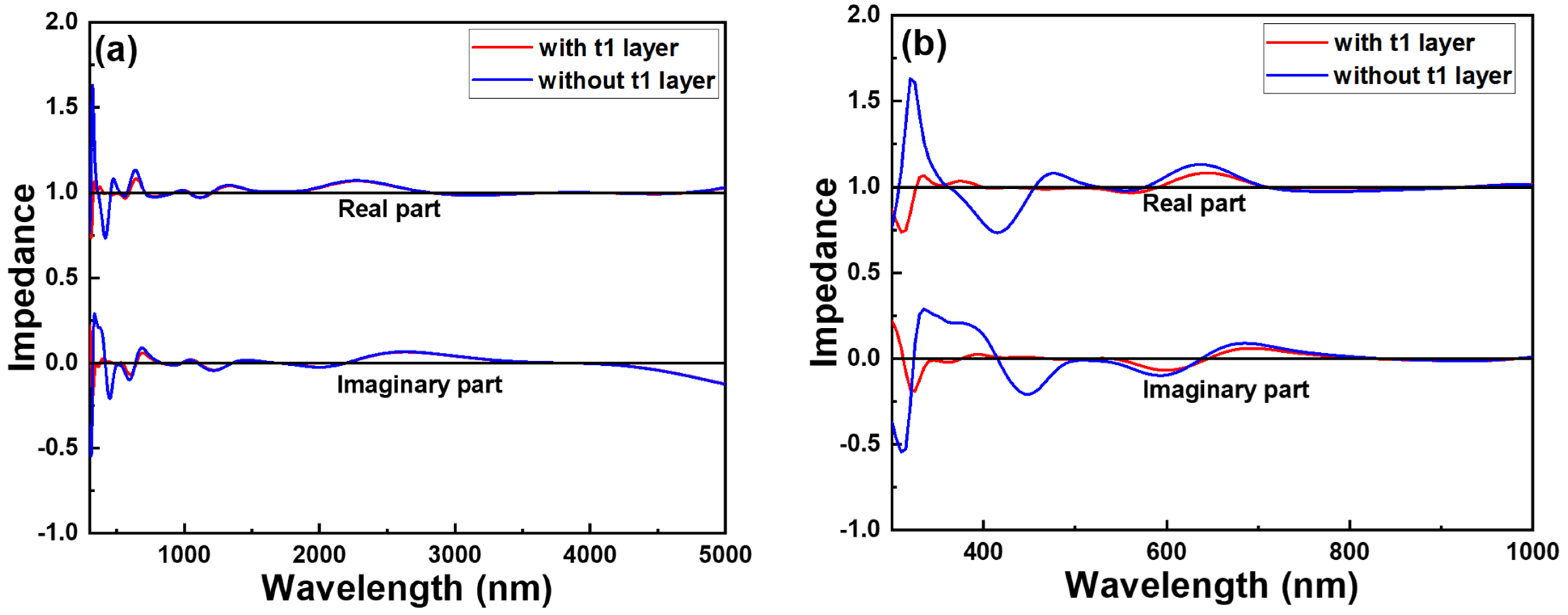
Optical impedance is a critical parameter used to characterize the propagation characteristics of light waves within a medium and their interaction with materials. It provides insights into the energy transfer and absorption behavior of light, finding wide applications in the field of optics. When the real part of the optical impedance of the top layer of an optical component approaches one and the imaginary part approaches zero in relation to air, it indicates that the surface of the optical component minimally obstructs light waves in the air. Essentially, the top layer scarcely absorbs or reflects light during its propagation. A real part close to one signifies that almost all light can penetrate or pass through the layer without being absorbed, while an imaginary part close to zero indicates minimal energy dissipation. In other words, light waves can enter or exit the optical component from or into the air almost unhindered, without significant reflection or absorption. This scenario is typically ideal in anti-reflection coatings or surface treatments as it minimizes light reflection to the greatest extent possible, facilitating efficient light propagation without energy loss or reflection.
Figure 9a depicts an extensive ultra-wideband spectrum ranging from 300 to 5000 nm, providing a broad view of optical behavior. Conversely,
Figure 9b offers a closer examination with a narrower spectrum spanning from 300 to 1000 nm, facilitating detailed analysis within a specific wavelength range.
In
Figure 9a, we observe that the optical impedance of both configurations closely aligns when the wavelength surpasses 820 nm. This indicates a similarity in optical response at longer wavelengths between both configurations. However,
Figure 9b reveals a significant departure from this alignment. Specifically, the real part of the structural impedance notably deviates from unity at wavelengths below 820 nm in
Figure 9b. Furthermore, the imaginary part displays a more pronounced departure from zero compared to the structure without the t1 layer. These observations indicate that the presence of the t1 layer influences the optical impedance, particularly at shorter wavelengths. This alteration in impedance suggests a modification in the absorptive characteristics of the structure, potentially resulting in enhanced absorptivity at shorter wavelengths. Thus, the inclusion of the t1 layer introduces a notable impact on the optical behavior of the system, emphasizing its significance in designing and optimizing optical devices or materials.
The impact of resonance effects on optical absorbers is crucial. Resonance effects can lead to localized enhancement of light, significantly increasing absorption rates. When light waves resonate with specific structures or materials of the absorber, resonance phenomena occur, resulting in a substantial enhancement of the absorber’s absorption for those particular wavelengths. For optical absorbers, surface plasmon resonance is a common resonance phenomenon. Surface plasmon resonance occurs when light waves interact with the oscillations of free electrons at the interface of a metal or semiconductor. By carefully designing the structure and materials of the absorber, the resonance frequency and intensity of surface plasmon resonance can be adjusted to achieve efficient absorption of light within specific wavelength ranges. In addition to surface plasmon resonance, other forms of resonance effects such as Fabry–Perot resonance may also impact the performance of optical absorbers. These resonance effects are typically controlled by adjusting the size, shape, and materials of the absorber to achieve selective absorption and enhancement of light. Therefore, efficient absorption and utilization of light within specific wavelength ranges can be achieved by designing and optimizing the structure and materials of the absorber to harness resonance effects.
Fabry–Perot resonance is indeed a resonance phenomenon based on the propagation of light between two reflecting interfaces. This resonance typically occurs within a cavity formed between two parallel reflecting interfaces. In the case of Fabry–Perot resonance, the effect is usually generated within the space formed between two reflective interfaces, which are primarily composed of materials with high reflectivity, such as metals, while the cavity itself is mainly composed of a dielectric material. The metallic layers could be made of materials like silver, copper, or gold, known for their good conductivity, while the dielectric layers could be materials like silicon dioxide or silicon nitride, known for their transparency. When light enters this cavity, it undergoes multiple reflections between the two interfaces, leading to interference upon each reflection. In common Fabry–Perot cavities, the enhancement of resonance intensity typically occurs within the dielectric layer. As the light waves bounce back and forth between the two reflecting interfaces, they establish standing wave patterns within the dielectric layer. When the wavelength of light aligns with the optical path length of the cavity at integer multiples, resonance occurs. This leads to a substantial increase in the intensity of the electric or magnetic field within the dielectric layer.
This enhanced field further intensifies the interaction between light and the material, thereby amplifying the resonance. Near the resonance wavelength, the electric or magnetic field intensity often experiences enhancement, indicating the localized effect of resonance at those wavelengths.
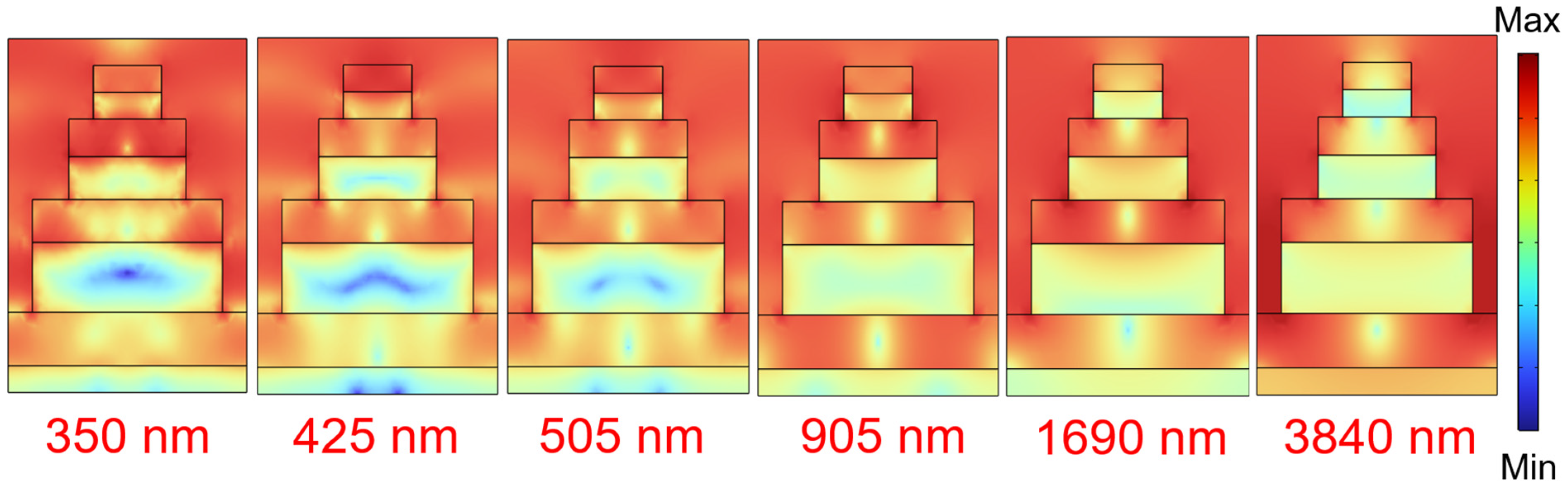
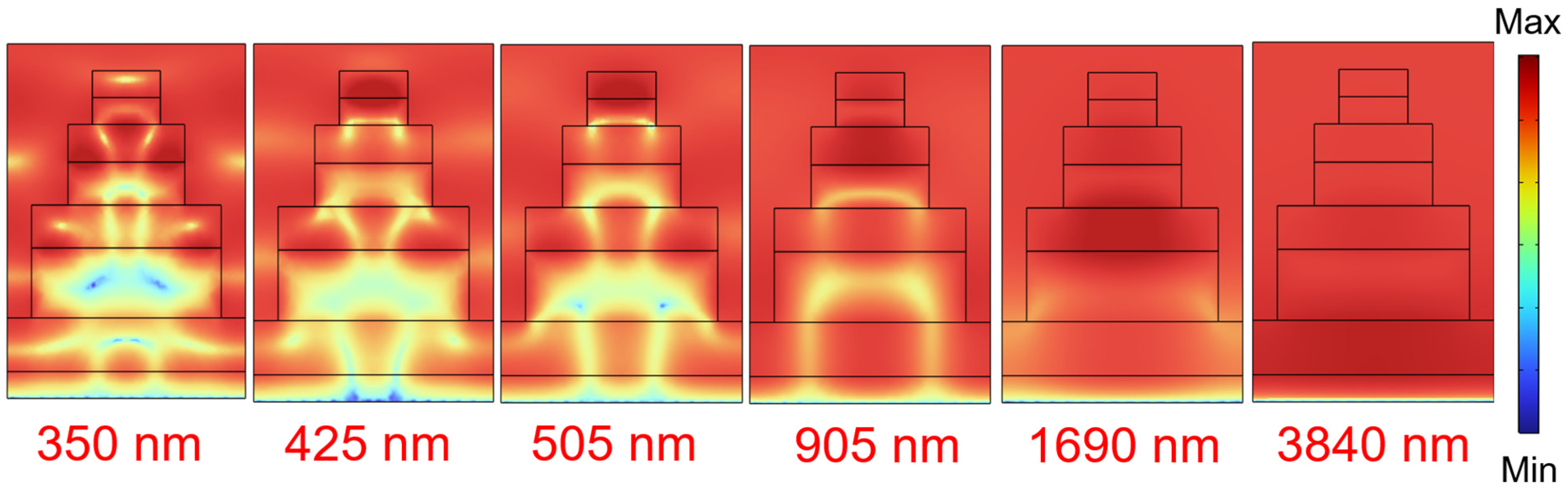
Figure 10 and
Figure 11 depict distributions of electric field intensities and magnetic field intensities under normal excitation of TE-polarized light at various wavelengths. Typically, when analyzing the distributions of electric and magnetic field intensities, the wavelengths chosen are those corresponding to the absorption peaks within the absorption spectra. Therefore, the selections of these specific wavelengths were informed by the absorption peaks identified in
Figure 2 of the absorption spectra. As shown in
Figure 10, enhancements in the electric field occur at different resonance peak wavelengths within the t3, t5, and t7 oxide layers. Therefore, Fabry–Perot resonance is also one of the principles contributing to achieving broadband and high absorptivity in this study.
Figure 10 also demonstrates that, while Fabry–Perot cavity effects occur at various wavelengths, the dielectric layer contributing to the most pronounced Fabry–Perot resonance varies. For instance, at an absorption peak of 350 nm, the most prominent Fabry–Perot cavity is observed within the t3 layer. However, at an absorption peak of 3840 nm, the most notable Fabry–Perot cavities are observed within the t7 layer. This indicates that as the wavelength of the absorption peak increases, stronger Fabry–Perot cavity effects occur within deeper layers of the dielectric material, away from the surface.
When the wavelength of the absorption peak increases, a stronger Fabry–Perot cavity effect occurs at deeper layers of the medium. This phenomenon is attributed to the relationship between the propagation characteristics of light in the medium and the optical path length within the cavity. As light propagates through the medium, it is influenced by the refractive index of the medium, causing the path of light to bend. The refractive index of the medium typically varies with the frequency of light waves, resulting in different propagation speeds and paths for light waves of different wavelengths within the medium. Specifically, longer wavelength light waves tend to bend more quickly within the medium, allowing them to reach deeper layers of the medium over shorter distances. On the other hand, the optical path length within the cavity is one of the key factors contributing to the Fabry–Perot cavity effect. Longer wavelength absorption peaks imply a longer optical path length within the cavity. This is because resonance conditions necessitate light waves to propagate back and forth multiple times within the cavity to form resonance phenomena.
Therefore, at longer wavelengths, light waves need to undergo more reflections and propagations within the cavity. This results in the involvement of deeper layers of the medium in the resonance effect, thereby increasing the importance of these deeper layers in generating stronger Fabry–Perot cavity effects. The observation of different dielectric layers contributing to Fabry–Perot resonance at different wavelengths suggests the importance of considering the optical properties and thicknesses of the layers in Fabry–Perot structures. It highlights the tunability of Fabry–Perot resonance by adjusting the structure and composition of the layers, which can be utilized in various applications. Additionally, understanding the depth-dependent nature of Fabry–Perot cavity effects can aid in optimizing the design of optical devices to achieve desired optical properties and performance across a broad range of wavelengths.
As depicted in
Figure 11, the Fabry–Perot cavity effect is less pronounced in the distributions of magnetic field intensities. However,
Figure 11 reveals that as the wavelength of the absorption peak increases, stronger magnetic field intensities occur at deeper layers of the metal and dielectric. However,
Figure 11 demonstrates that as the wavelength of the absorption peak increases, stronger magnetic field intensities occur at deeper layers of both the metal and dielectric, not solely within the dielectric layer. Therefore, it is not solely attributed to the Fabry–Perot cavity effect. There could be various reasons for this phenomenon, including interface effects, surface plasmon resonance effects, and multimode resonance effects. As previously mentioned, the presence of multimode resonance effects was observed in the t8-t7 layers. Multimode resonance may arise due to the complexity of the structure or interactions between different modes. When light waves interact with multiple modes within the structure, multimode resonance effects may occur, leading to localized enhancements in the magnetic field. This indicates that the stronger magnetic field intensities observed at deeper layers of both the metal and dielectric as the wavelength of the absorption peak increases are caused by multimode resonance effects.
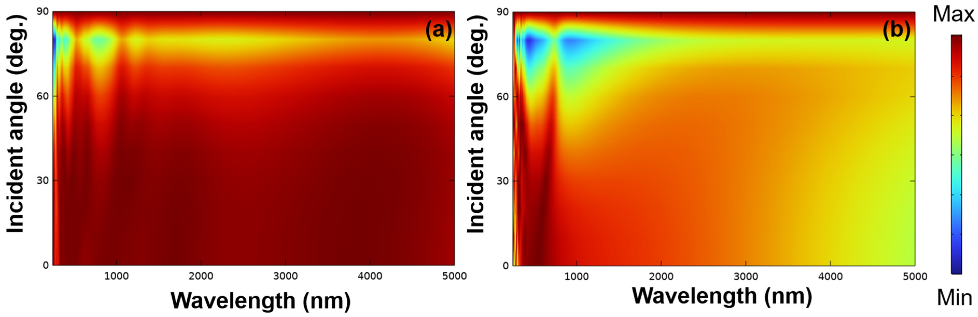
The simulation results vividly demonstrate the exceptional absorptive capabilities of the pyramid-like absorber under study, outperforming many other absorbers previously investigated. This notable advancement can be attributed to several factors, including enhancements in surface plasmon resonance, interference effects among different layers and materials, the Fabry–Perot cavity effect, and multimode resonance phenomena spanning the analyzed wavelength spectrum. One critical factor influencing the performance of optical absorbers, particularly in the realm of thin-film or nanostructured materials, is the angle of incident light. The significance of a wide incident light angle on optical absorbers lies in its ability to enhance light capture, broaden the spectrum of absorbed wavelengths, reduce reflectance, and ensure consistent performance regardless of the angle of incidence. In essence, the comprehensive understanding of these intricate mechanisms not only highlights the efficacy of the pyramid-like absorber but also underscores the importance of considering various factors, such as incident light angle, in optimizing the performance of optical absorbers for diverse applications.
An optical absorber that maintains optimal functionality regardless of the angle of incidence proves to be highly reliable in various applications. To assess its absorption characteristics comprehensively, evaluations were conducted across incident light angles ranging from 0° to 90°, considering both TE and TM polarizations. The results are illustrated in
Figure 12. Under TE polarization and within the wavelength range of approximately 335 to 1000 nm, the investigated pyramid-like absorber exhibited absorptivity exceeding 90% over an angular range of 0° to 62°. This exceptional performance extended further to 0–74 degrees within the wavelength range of approximately 1000 to 5000 nm. Similarly, under TM polarization and within the wavelength range of approximately 335 to 800 nm, the absorber showcased absorptivity exceeding 90% over an angular range of 0° to 55°. Furthermore, within the wavelength range of approximately 800 to 3800 nm, the angular range of absorptivity exceeding 90% extended to 0–43°. These findings underscore the remarkable insensitivity of the designed pyramid-like absorber to incident angles, particularly in the ultraviolet A to middle-IR region. Moreover, the absorber’s highly symmetrical structure contributes to its polarization-independent nature, enhancing its overall absorption performance. This comprehensive analysis provides valuable insights into the robustness and versatility of the pyramid-like absorber, positioning it as a promising candidate for a wide range of optical applications.
When the angle of incident light exceeds 60°, there is a sudden and rapid decrease in absorptivity, a phenomenon that has been less discussed in the past. However, as the angle of incident light increases beyond 60°, the propagation of light within the material may undergo a change, potentially leading to a decline in the efficiency of light propagation within the absorbing material and consequently causing a sudden, rapid decrease in absorptivity. One possible reason is the occurrence of total internal reflection when light rays enter the absorbing material at larger angles. In such cases, the incident light is completely reflected back along the interface of the material rather than being absorbed. This allows the light to escape without absorption, thereby reducing the absorptivity. Additionally, when light enters the absorbing material at larger angles, the optical path length within the material increases. This may increase the chances of light being scattered or absorbed, resulting in a decrease in absorptivity. Another possible reason is the bandgap effect, where some materials exhibit effective absorption of light only at specific wavelengths and angles of incidence. As the angle of incidence increases, the bandgap effect may lead to a sharp decrease in the absorptivity of light. In essence, when the angle of incident light exceeds 60°, these factors may collectively contribute to a sudden, rapid decrease in the absorptivity of light within the absorbing material.
To highlight the advantages of this work,
Table 2 compares the results of this study with the characteristics of several ultra-wideband absorbers published in the past two years. As shown in
Table 2, compared to these broadband solar absorbers, the bandwidth of our researched solar absorber does not extend to wavelengths close to 250 nm. However, our absorber achieves an absorptivity exceeding 0.900 over a range reaching 355 nm. Additionally, our absorber achieves an absorptivity exceeding 0.900 over a range reaching 4865 nm, with an average absorptivity in the range of 355–4865 nm reaching 0.966. The simultaneous presence of an ultra-wide bandwidth at 4510 nm and a high absorptivity of 0.966 is rarely achieved by solar absorbers.


