Article

Shallow Trench Isolation Patterning to Improve Photon Detection Probability of Single-Photon Avalanche Diodes Integrated in FD-SOI CMOS Technology

1
INSA Lyon, Ecole Centrale de Lyon, CNRS, Université Claude Bernard Lyon 1, CPE Lyon, INL, UMR5270, 69621 Villeurbanne, France
2
Universite Claude Bernard Lyon 1, INL, UMR5270, CNRS, INSA Lyon, Ecole Centrale de Lyon, CPE Lyon, 69622 Villeurbanne, France
3
ICube Research Institute, University of Strasbourg and CNRS, 23 Rue du Loess, 67037 Strasbourg, France
4
STMicroelectronics, 38920 Crolles, France
*
Author to whom correspondence should be addressed.
Photonics 2024, 11(6), 526; https://doi.org/10.3390/photonics11060526
Submission received: 22 March 2024 / Revised: 29 May 2024 / Accepted: 30 May 2024 / Published: 1 June 2024
(This article belongs to the Special Issue Emerging Topics in Single-Photon Detectors)

Abstract

:
The integration of Single-Photon Avalanche Diodes (SPADs) in CMOS Fully Depleted Silicon-On-Insulator (FD-SOI) technology under a buried oxide (BOX) layer and a silicon film containing transistors makes it possible to realize a 3D SPAD at the chip level. In our study, a nanostructurated layer created by an optimized arrangement of Shallow Trench Isolation (STI) above the photosensitive zone generates constructive interferences and consequently an increase in the light sensitivity in the frontside illumination. A simulation methodology is presented that couples electrical and optical data in order to optimize the STI trenches (size and period) and to estimate the Photon Detection Probability (PDP) gain. Then, a test chip was designed, manufactured, and characterized, demonstrating the PDP improvement due to the STI nanostructuring while maintaining a comparable Dark Count Rate (DCR).

1. Introduction

Single-Photon Avalanche Diodes (SPADs) have become the most-used photodetectors for so-called “time of flight” measurement in the near-infrared domain thanks to their high sensitivity and high speed [1,2,3]. SPADs are easily integrated into CMOS technologies to cover wavelengths from 500 to 950 nm, particularly for facial recognition and telemetry applications. Other scientific and medical imaging applications have been successfully achieved using SPAD features, as described in [4,5,6,7]. State-of-the-art SPADs use a 3D integration approach at the wafer level with backside illumination. The current work focuses on the development of large SPAD arrays with low pitch and very low noise [8,9].
One of the key figures of merit of SPAD devices is the Photon Detection Probability (PDP), which has led to important research studies. The PDP represents the SPAD devices’ sensitivity and is defined as the probability of an absorbed incident photon to generate an avalanche event. The PDP is a function of the photogeneration rate and triggering probability and depends on the SPAD architecture, e.g., the doping levels and operating conditions such as the photon wavelength and reverse bias voltage. In order to improve the PDP of SPADs integrated in CMOS technologies, the authors in [10,11,12], respectively, employ the following approaches: (i) an optimized SPAD architecture with charge focusing, (ii) an increase in the light–material interaction due to nanostructuration, and (iii) a germanium cavity as an absorption layer.
As an alternative, the implementation of SPADs in Fully Depleted Silicon-On-Insulator (FD-SOI) CMOS technology has been developed with the aim of obtaining a 3D SPAD pixel at the chip level with backside illumination (BSI) for near-infrared light (NIR) [13,14] or frontside illumination (FSI) for visible and NIR light. SPAD FD-SOI devices are implemented below the buried oxide (BOX) layer and the electronic logic circuits are inserted into the thin silicon layer on top of the BOX layer, which provides an intrinsic 3D stack and a much higher fill factor considering BSI. Different architecture variants were studied to assess the impact of the Shallow Trench Isolation (STI) location and density on the performance of the SPAD FD-SOI, particularly in terms of the Dark Count Rate (DCR) and PDP [15]. Experimental measurements correlated with simulation results on SPADs FD-SOI with non-passivated STI trenches have shown that the overall DCR increases with STI density at high excess voltage [16]. There are very few ways of improving the PDP of the SPAD FD-SOI, when only minor technological modifications are possible. However, the electro-optical simulations presented in [17] show that STI nanostructuration can be used to improve the PDP for FSI. In this article, we study the DCR and FSI PDP measured on a SPAD implementing STI nano-patterning and we compare the results with measurements from a reference SPAD. The following section presents the SPAD FD-SOI architecture, the constructive interference concept, the design methodology, and the fabricated test chip.

2. Materials and Methods

2.1. SPAD FD-SOI Architecture and Constructive Interferences

2.1.1. SPAD Integrated in FD-SOI CMOS Technology

The schematic cross-section of the SPAD FD-SOI is shown in Figure 1. The diode (25 µm in diameter in our case) is located between the Deep N-well (cathode) and P-well (anode) junction. The thin BOX separates the diode from the active silicon layer containing the MOSFET transistors. Then, we can consider FSI for visible and NIR light (removing all BEOL metallic layers and transistors on top the photosensitive active area) or BSI for NIR light after die thinning (tacking benefit of the native 3D staking at die level). In our case, FD-SOI CMOS technology is fixed and does not include any specific steps for photonics applications such as antireflective coatings, micro-lenses, etc. The range of techniques for improving the PDP is therefore very limited. We have identified the possibility of improving the PDP in FSI by nanostructuring an existing layer without modifying the technological process, as presented in the following section.

2.1.2. Constructive Interferences with STI Patterning (for FSI)

Due to the design rules of the technology and as shown in Figure 1, some STI is natively present in the SPAD cell (trenches in the P-well layer). However, as illustrated in the structure shown in Figure 2, this study aimed to increase the FSI light sensitivity with an optimized STI layer layout (size and period) allowing both antireflection and light–silicon interaction enhancement. Therefore, we used these blocks of STI, precisely choosing their dimensions and positions, to create a photonic crystal layer (diffraction grating) providing constructive interference effects, in order to locate the maximum interference in the Space Charge Region (SCR) [17].

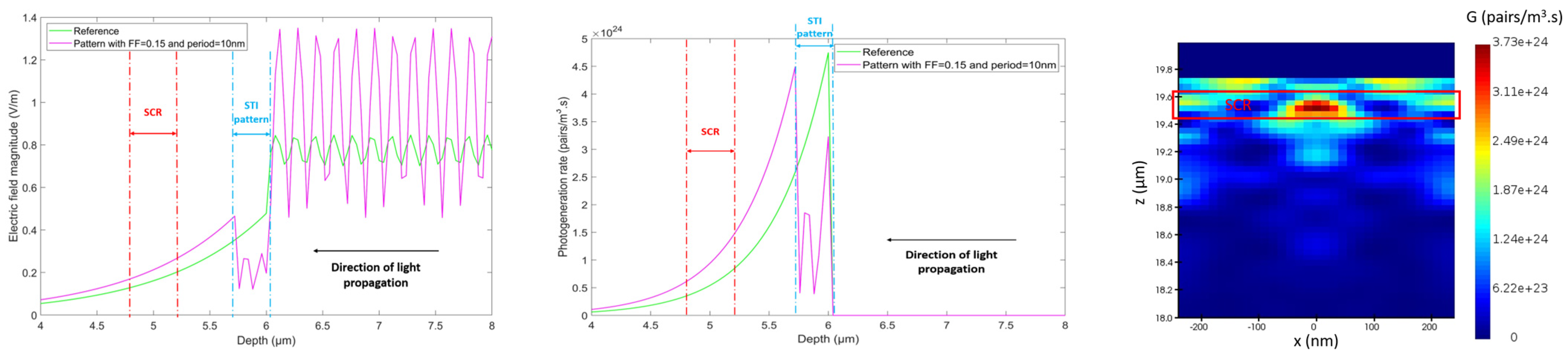
2.2. STI Nanostructuration Optimization

From the optical point of view, the SPAD structure could be simplified as shown in Figure 2c, where the SiO2 region and silicon substrate region are considered semi-infinite. The problem of improving the photon detection efficiency with a diffraction grating comes down to maximizing the light intensity in the SCR (multiplication region).
As the silicon substrate is sufficiently thick to be considered infinite due to its high absorption of visible light, it is not possible to use the concept of light trapping by coupling the light with a waveguide mode or to use a metallic back reflector as realized for thin detector configurations. This optimization is thus realized in two steps. Firstly, the pattern plays the role of an antireflection coating (considering FSI) to minimize the reflection coefficient R 1 at the SiO2/diffraction grating interface. R 1 is a function of the optical index n 1 , n 2 , n 3 and the diffraction grating thickness t 2 . The equivalent optical refractive index n 2 , e q in the case of FSI follows an effective medium law at normal incidence [18]:
n 2 , e q 2 = n S i O 2 2 · 1 F F + n s i l i c o n 2 · F F
where FF is the fill factor, defined as the ratio between the silicon area and the total area of one STI periodic pattern (here, squared shapes are used). The equivalent optical index of the diffraction grating layer is thus a function of F F that should be chosen to minimize light reflection. The second step consists of choosing the grating period T in a such way that −1 and +1 orders of diffraction produce an interference pattern to confine the maximum light intensity in the SCR where the avalanche triggering probability is the highest. The position of the maximum interferences is a function of the pattern period and the photon wavelength. Suitable pattern periods allow for an improvement in the photogeneration rate in the SCR and thus an improvement in the PDP for a certain wavelength range. To choose a starting value for the simulations before optimization (described in the next section), the vertical positions z m of the maximum light intensity can be estimated by considering normal incidence using the expression below:
z m = λ n s i l i c o n · 1 1 λ T · n s i l i c o n 2
where λ is the photon wavelength, T the STI pattern period (supposedly identical in x and y directions) and n s i l i c o n the real component of the silicon refractive index.

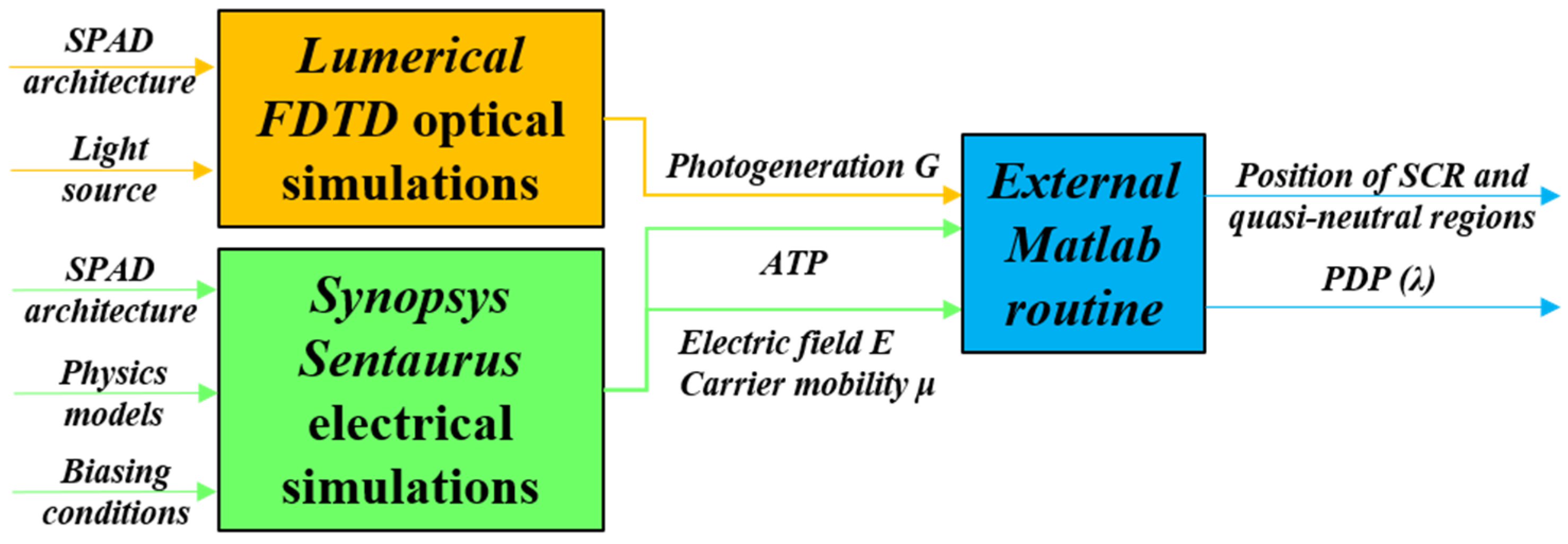
2.2.1. Simulation Framework and Assumption

In order to estimate the P D P of SPAD devices, we integrated the product of the avalanche triggering probability ( A T P ) and the local electron–hole photogeneration rate ( G ) over the active volume ( V ) of the SPAD. Then, we divided this by the incident photon flux Φ p h o t o n s (number per second) at the considered wavelength λ :
P D P λ = 1 Φ p h o t o n s λ A T P x , y , z × G x , y , z ,   λ   d V
The simulation flow was then divided into two parts: the electrical part and optical part. We performed the electrical and optical simulations with Synopsys Sentaurus and Lumerical FDTD, respectively, to obtain both the electrical data ( A T P , electric field E , carrier mobility μ ) and optical data (photogeneration rate G ). It is important to point out that this photogeneration rate depends on many factors. For a fixed incident illumination, this parameter mainly depends on the way the light is manipulated within the structure. Thus, this photogeneration rate is the consequence of multiple interferences in the direction of the substrate and in the plane of the SCR: the optimization of the STI geometry can be used to maximize G over the SCR. Data are combined and postprocessed using an external Matlab routine, as shown in Figure 3. We considered that the SPAD was composed of the SCR (multiplication region) and two quasi-neutral regions: one p-type doped on top of the SCR and the other n-type doped below the SCR. We calculated the limits of the active region (where photogenerated carriers effectively lead to an avalanche event) by analyzing the electric field distribution across the structure and also the ratio of drift and diffusion velocities of minority carriers in each quasi-neutral region to consider the contribution of these regions to the PDP [17]. The simulation methodology was applied to SPAD FD-SOI, bearing in mind the following:
  • STI blocks have a depth defined by the technological process and must respect the process design rules in terms of width, length, and spacing.
  • The FSI is adversely affected by the presence of Back-End-Of-Line (BEOL) layers, which are not optimized for optical light transmission (moreover, their optical properties are not fully characterized).
Nevertheless, the optimization strategy, presented in the next section, still remains effective.

2.2.2. Optimization Methodology

Our simulation methodology firstly involves finding the optimal F F of the STI, which allows for the maximum light transmission by performing optical simulations with a small pattern period (less than 100 nm). Once the optimal F F is found, the second step is to extract the optimal spatial period allowing for constructive interferences in the SCR.
In the first step, several values of F F were simulated at two specific wavelengths (500 nm and 650 nm) to save simulation time. Figure 4 presents the profiles of the electric field magnitude and photogeneration rate with F F = 0.15 at wavelength of 500 nm and with a pattern period of 10 nm for patterned or non-patterned structures. These profiles were extracted near the center of one STI pattern for an incident light power of 1 W/m2. The curves show a significant antireflection effect of the patterned STI ( F F = 0.15) as compared to the reference structure, with relative improvements of up to 30% and 60% for the electric field magnitude and photogeneration rate, respectively. It is worth mentioning that a more pronounced antireflection effect could be obtained if some constraints of the STI patterns design rules could be released by the foundry.
The second step was dedicated to the optimization of the pattern period in order to locate the maximum interferences in the SCR. Numerous simulations varying the pattern period for each F F value were launched. Figure 4 on the right illustrates the cartography of the photogeneration rate at wavelength of 500 nm with a 0.48 µm periodic pattern and F F of 0.15. The SCR was located 180 nm away from the diffraction grating/silicon substrate interface. We could observe the presence of a hotspot in the SCR, clearly showing the diffracting effect of the pattern.
These period dimensions were then used in the simulations with a larger range of wavelengths at 400–1000 nm in order to investigate the improvement with visible to near-infrared light. Figure 5 illustrates the P D P profiles with excess voltages V e x of 0.6 V and 1.5 V, respectively (i.e., 6% and 15% of V b d , the breakdown voltage). The second value of V e x allows for higher values of A T P and consequently of P D P , and thus a greater difference between the patterned and reference SPAD. The curves show a clear relative improvement in the P D P for shorter and longer wavelengths. However, for mid-range wavelengths, the gain in P D P is relatively smaller with higher absolute values of P D P . The relative gain could reach 700% at specific wavelengths and the average relative gain could reach over 100% in the considered range of wavelengths.
Thanks to these simulation results, we have selected a pattern period (pitch) of 480 nm associated with three patterns’ F F (i.e., 15%, 20% and 25%) for IC fabrication and for future characterizations. As an example, the STI pattern parameters corresponding to 480 nm pitch and 15% of the pattern fill factor (silicon area over total area) is realized with squares of 186 × 186 nm2 SOI stacks separated by 294 nm STI trenches.

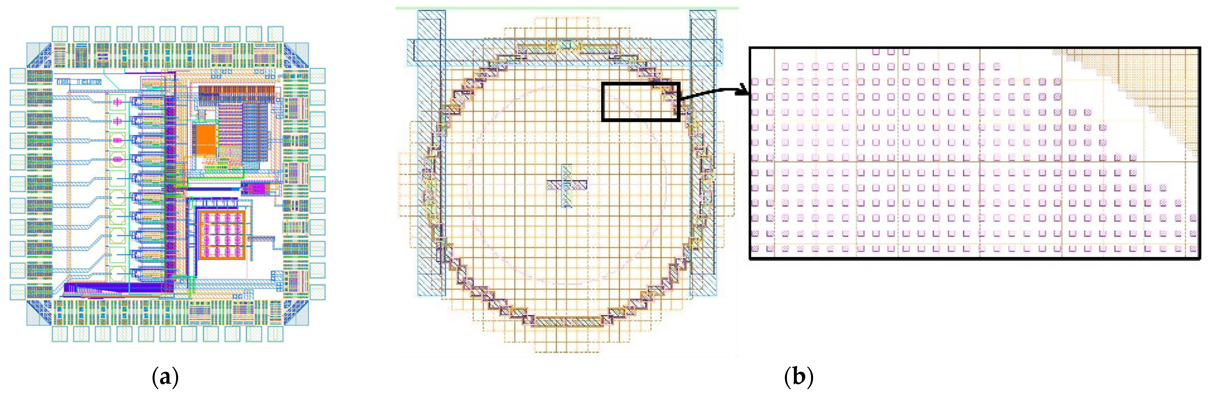
2.3. Test Chip Presentation

A test circuit was designed and fabricated in 28 nm CMOS FD-SOI technology (Figure 6a), incorporating several variants of SPADs (reference, STI patterning with various F F , etc.) with associated electronics for active quenching and recharging. Figure 6b illustrates the layout of a quasi-circular SPAD with an inset showing the STI patterning above the photosensitive area. The standard process was used (except for the modified Deep N-well implantation [15]) including all BEOL layers but no antireflective coating (ARC) or micro-lenses were implemented. We can assume that very little light reaches the CMOS electronics because all the Back-End-Of-Line (BEOL) layers (including the metallic dummy structures) are present and screen the light. Only the photosensitive areas above the SPADs are open (no metallic BEOL layers) to let light through. It is noted that in our study, the impact of parasitic illumination on and from the CMOS regions can be neglected because (i) all the BEOL layers (including the metallic dummy structures) are present above the CMOS regions and screen the light, and (ii) for the photosensitive areas above the SPADs where there are no metallic BEOL layers to let light pass through, reflections at the STI/Si interfaces protect the CMOS from photons reflected at the Si/Box interfaces. The schematic diagram of the electronics is shown in Figure 7a. The SPAD is associated with on-chip quench and recharge electronics, which are controlled by an external FPGA board enabling the dead time to be adjusted. The events can be observed either through the digital output or the analog output using an integrated wide-band amplifier (Figure 7b). The SPAD FD-SOI breakdown voltage V b d is around 15.8 V at room temperature (extracted with IV reverse curve directly measured on the diode), whereas the minimum reverse voltage leading to the first detected avalanche events (called V H V 0 ) is ≈16.1 V, taking into account the detection threshold of the embedded on-chip electronics. The following section presents the experimental results and analysis.

3. Results

All the measurements presented in the following sections (DCR and PDP) are made in the active quench and active recharge mode, with a total dead time around 1.1 µs, which can be divided into 40 ns for the signal propagation delay and the FPGA board response time, 1 µs of active quench forced by the FPGA (AQ active and AR inactive) and about 20 ns of recharge forced by the FGPA (AR inactive and AQ active) before SPAD release (AR inactive and AQ inactive).

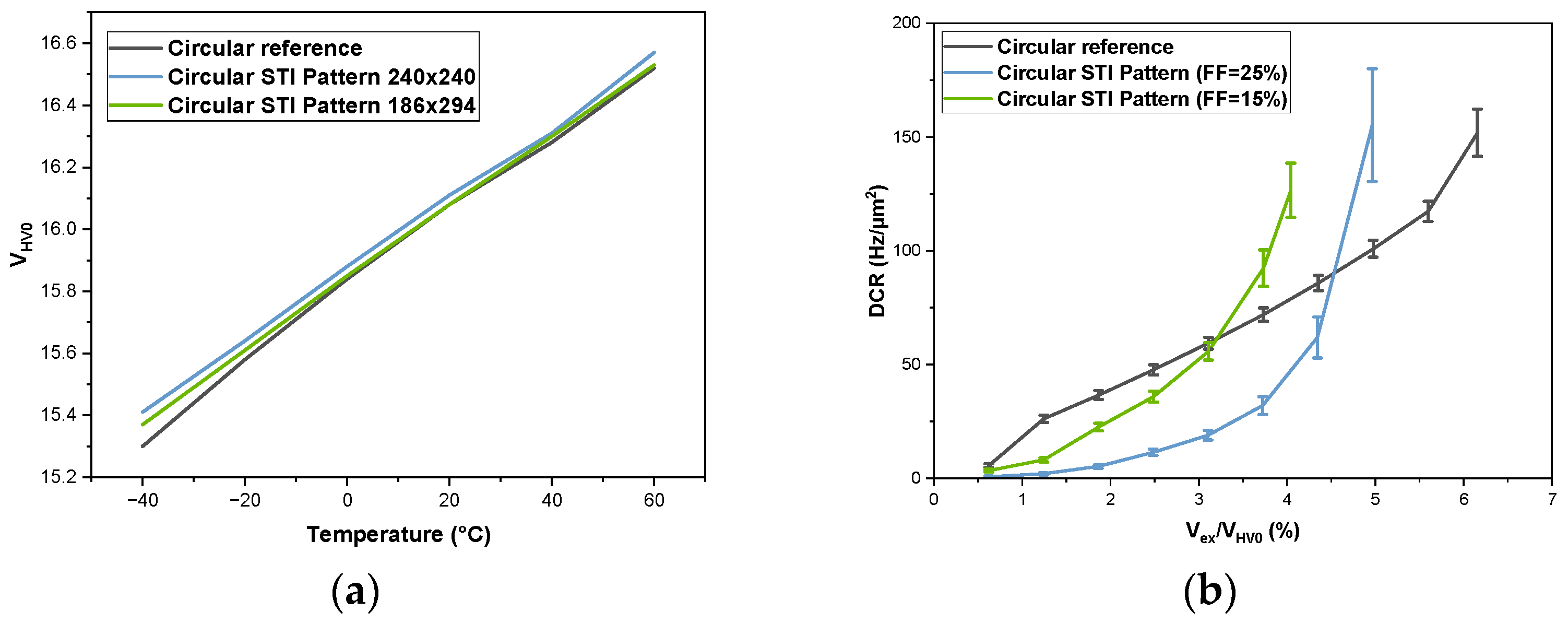
3.1. Dark Count Rate (DCR) Experimental Results

Figure 8 shows V H V 0 as a function of the temperature and the measured DCR as a function of the excess voltage for a quasi-circular reference SPAD and for SPADs with the same geometry and the addition of the STI patterning above the sensing region (with F F = 15 and 25%), both acquired with a 1.1 µs dead time. In this figure and all those presented in this article, the error bars are defined as the standard deviation of the measured values for a single characterized device. Firstly, the threshold voltage V H V 0 increase with temperature (+11 mV/°C) is a signature of the impact ionization avalanche mechanism in the SPAD multiplication zone. The increase in the DCR with excess voltage is more abrupt in the presence of STI patterning due to afterpulsing runaway, as observed in previous studies [15,16]. This phenomenon will have the effect of limiting the maximum excess voltage to around 0.65 V (4% of breakdown voltage V b d ) for F F = 15% and to around 0.8 V (5% of V b d ) for F F = 25%.
Figure 9 presents the Arrhenius DCR plots and shows that the DCR increases with temperature for both the reference and patterned SPAD. The extracted activation energy around 0.25 eV ± 0.05 eV suggests that noise mechanisms may be a combination of thermal generation and a band-to-band mechanism associated with field-enhanced trap-assisted tunneling effects. The exploding DCR for the patterned SPAD above V e x , m a x = 0.65 V or 0.8 V can be related to the high generation rate due to defects at the STI interface, including trap-assisted thermal generation and afterpulsing. Afterpulsing describes how an electron or a hole created during the avalanche can be captured by a trap and released at the end of the quench and recharge cycle, generating a new avalanche. It is important to note that comparable DCR levels for both structures (reference and patterned) are observed below V e x = 0.7 V, i.e., 5% of V b d (Figure 8b).

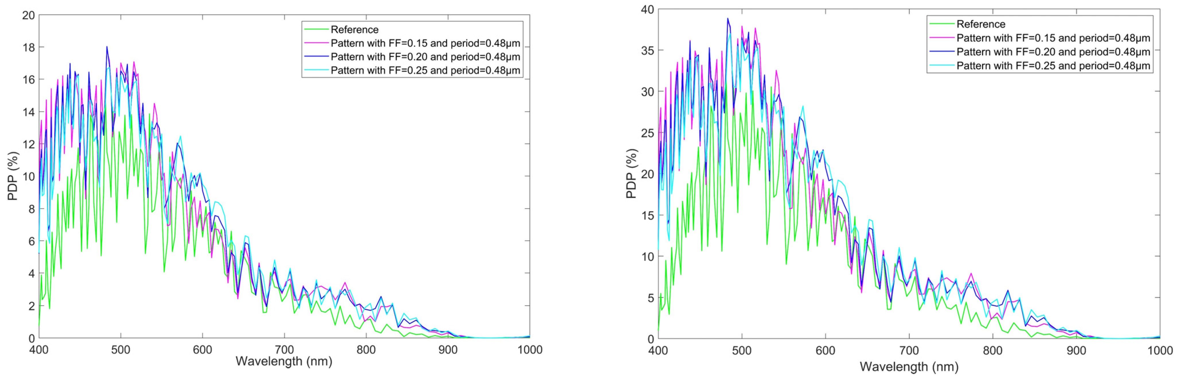
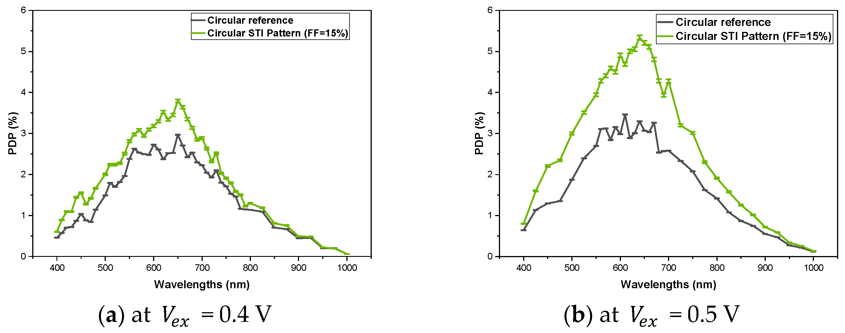
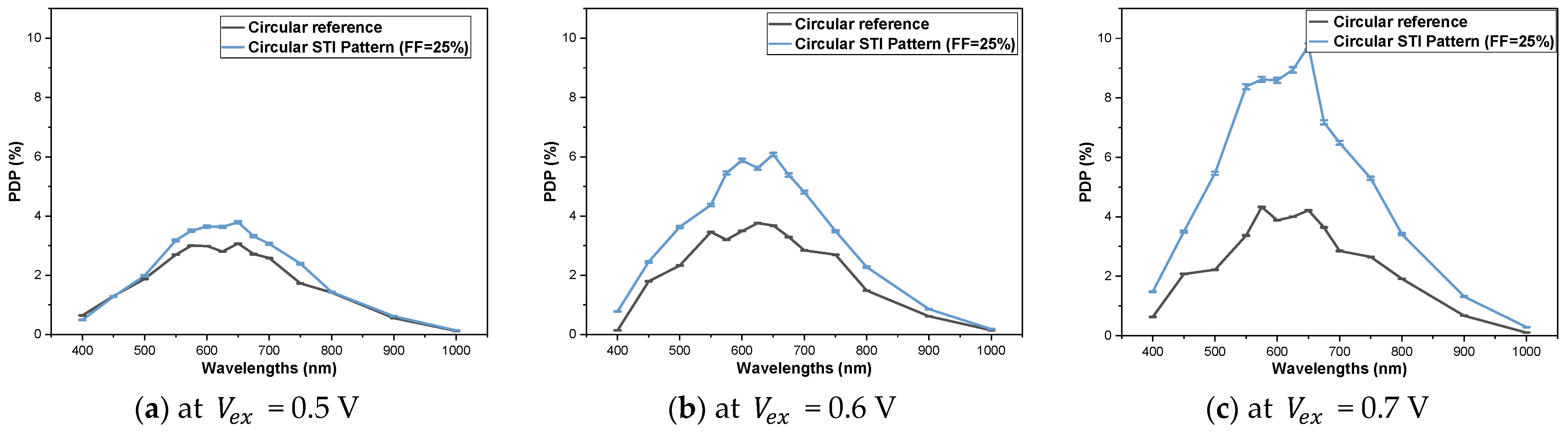
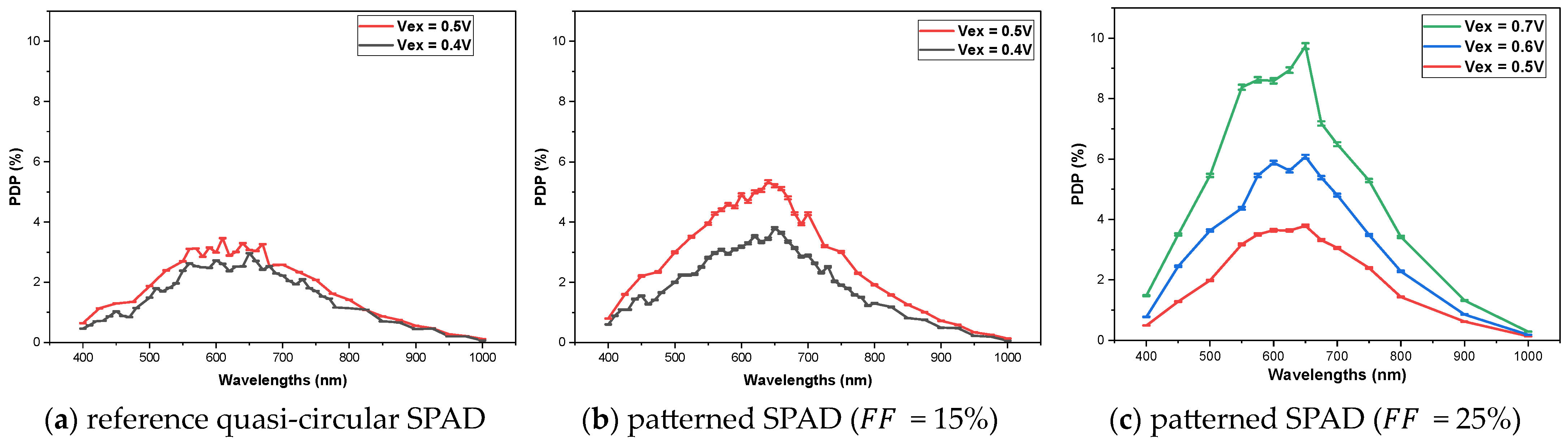
3.2. Photon Detection Efficiency (PDP) Experimental Results

The experimental PDP was obtained using an integrating sphere setup for the simultaneous measurements of a calibrated SPAD ($PD-050-CTB, Micro Photon Devices) and the device being tested. To obtain this PDP, the number of avalanche events is counted with and without illumination. The difference in the number of events compared with that of a calibrated commercial SPAD is calculated to give the absolute efficiency. During this PDP measurement, all the SPADs are illuminated with the same light intensity. The benefit of STI patterning compared to the reference SPAD is confirmed in Figure 10 and Figure 11 for pattern F F = 15% and 25%, respectively. The PDP is measured over a V e x range from 0.4 V (2.5% of V b d ) to 0.7 V (4.4% of V b d ), where the DCR levels are comparable (Figure 8b). Note that the absolute values of the PDP remain low due to the use of a standard process (presence of all the BEOL layers without ARC coating). Table 1 summarizes the PDP relative gains at the peak sensitivity (i.e., λ~645 nm) and the average PDP relative gains along the spectrum for different excess voltages and F F linked to the STI patterning. It should be noted that the measurements were carried out on the reference and patterned SPADs from the same chip (i.e., minimizing any difference resulting from process mismatch) and confirmed by the measurements on several cells available on this chip.

4. Discussion

The experimental increase in the PDP for the patterned structure confirms the benefits of the proposed constructive interference approach by nanostructuring the STI layer. It is difficult to quantitatively compare the measured increase in the PDP with the values estimated using the simulations in Section 2 due to the approximations made in the methodology (e.g., the quantification of the photogenerated carriers outside the SCR) and to the large number of estimated parameters (such as the optical coefficients of the BEOL layers).
Through analyzing the results presented in the previous section, one can note that the relative PDP gain (compared to the reference SPAD) obtained with STI patterning above the light-sensitive region of the SPAD increases with V e x (from 28% at V e x = 0.4 V to 62% at V e x = 0.5 V for F F = 15%, and from 23% at V e x = 0.5 V to 131% at V e x = 0.7 V for F F = 25%). Furthermore, comparing the PDP measured at V e x = 0.5 V to V e x = 0.4 V, the patterned SPAD with F F = 25% presents a greater relative PDP gain (45%) than the reference SPAD (18%), as is clearly observable in Figure 12a,b. Similarly, the relative gain in the PDP when increasing V e x for the patterned SPAD with 25% F F is also much greater than that of the reference SPAD (Figure 12c). This higher relative gain increase with excess voltage for the patterned SPAD compared to the reference structure can be partially explained by the higher increase in (i) the avalanche triggering probability P t , and in (ii) the number of photogenerated carriers. Indeed, according to a previous TCAD study [15], a greater increase in P t with excess voltage can be expected for patterned SPADd due to the STI trenches close to the multiplication region. Additionally, an increase in the photogenerated carriers can also be expected due to the slight extension of the depleted zone (SCR in Figure 2) into a region containing a larger concentration of photons due to light focusing in the patterned SPAD. The improvement in the PDP, which is much larger than that obtained in Section 2 and the simulation study in [17], is not fully explained. Afterpulsing could contribute to an overestimation of the PDP gain when increasing the excess voltage. The simulation study was conducted with rigor, but it could be improved with the following suggestions, which may explain the differences with the experimental results: (i) the optical simulation only concerns normal incidence; (ii) in the calculation of the PDP, we have always used the same ATP map (obtained without STI patterning), so we only quantify the contribution related to the light concentration under a normal incidence; (iii) taking into account the photogenerated carriers in the regions close to the SCR (quasi-neutral zones) is delicate and complicated. Some approximations and choices have been made to account for this contribution, but this part could be reviewed and improved. It should also be mentioned that, despite the significant improvement in the PDP measured thanks to the STI patterning, this PDP does not reach the level of the PDP reported in the literature for state-of-the-art SPADs. In our study, we use native FD-SOI CMOS technology, which is not specifically adapted to photonic applications and therefore does not include technological options such as antireflection coatings, micro-lenses, etc. In addition, the presence of all the dielectrics of the BEOL above the active area of the SPAD reduces the light transmission. The PDP levels therefore remain below the state of the art, but the STI nanostructuring approach would be all the more effective if it could be implemented in a process optimized for photonics.

5. Conclusions

The SPAD FD-SOI concept is particularly useful for backside illumination in the near-infrared range after the device has been thinned. Nevertheless, in this study, we demonstrate that the SPAD FD-SOI is promising for frontside illumination (visible or near-infrared light). The STI trenches above the photosensitive area can be used to benefit from the constructive interference and improve the PDP while maintaining an equivalent DCR. This study was carried out on a standard non-photonics-dedicated manufacturing process in which the SPAD implemented under the BOX layer was designed within the constraints of the design rules. It is clear that an optimized process would greatly improve the performance of the SPAD FD-SOI to reveal the potential of such an approach.

Author Contributions

Conceptualization: S.G., F.M., R.O. and F.C.; methodology: S.G., F.M., R.O. and F.C.; software: S.G., F.M. and R.O.; measurements: S.G., D.-T.V. and F.C.; IC design: M.D.L., J.-B.S., J.-B.K., W.U. and S.G.; analysis: S.G., F.C., T.C., F.M., R.O. and D.-T.V.; writing—original draft preparation: F.C. and D.-T.V.; writing—review and editing: F.C., P.P., M.L.B., T.C., F.M. and R.O.; supervision: F.C.; project administration: F.C.; funding acquisition: F.C., A.C. and D.G. All authors have read and agreed to the published version of the manuscript.

Funding

This research was funded by the Nano2022 research program, the French national research agency ANR (ANR-18-CE24-0010), and the France 2030 program.

Institutional Review Board Statement

Not applicable.

Informed Consent Statement

Not applicable.

Data Availability Statement

Data is contained within the article.

Acknowledgments

The authors would like to thank CMP (Grenoble) for the IC prototyping services.

Conflicts of Interest

The authors declare no conflicts of interest.

References

  1. Gyongy, I.; Erdogan, A.T.; Dutton, N.A.; Martín, G.M.; Gorman, A.; Mai, H.; Della Rocca, F.M.; Henderson, R.K. A Direct Time-of-Flight Image Sensor with In-Pixel Surface Detection and Dynamic Vision. IEEE J. Sel. Top. Quantum Electron. 2023, 30, 3800111. [Google Scholar] [CrossRef]
  2. Pellegrini, S.; Buller, G.S.; Smith, J.M.; Wallace, A.M.; Cova, S. Laser-based distance measurement using picosecond resolution time-correlated single-photon counting. Meas. Sci. Technol. 2000, 11, 712–716. [Google Scholar] [CrossRef]
  3. Martin, F.; Mellot, P.; Caley, A.; Rae, B.; Campbell, C.; Hall, D.; Pellegrini, S. An all-in-one 64-zone SPAD-based Direct-Time-of-Flight Ranging Sensor with Embedded Illumination. In Proceedings of the 2021 IEEE Sensors, Sydney, Australia, 31 October–3 November 2021; pp. 1–4. [Google Scholar] [CrossRef]
  4. Charbon, E. Single-photon imaging in complementary metal oxide semiconductor processes. Philos. Trans. R. Soc. A 2014, 372, 20130100. [Google Scholar] [CrossRef] [PubMed]
  5. Pancheri, L.; Ficorella, A.; Brogi, P.; Collazuol, G.; Betta, G.-F.D.; Marrocchesi, P.S.; Morsani, F.; Ratti, L.; Savoy-Navarro, A.; Sulaj, A. First Demonstration of a Two-Tier Pixelated Avalanche Sensor for Charged Particle Detection. IEEE J. Electron Devices Soc. 2017, 5, 404–410. [Google Scholar] [CrossRef]
  6. Henderson, R.K.; Johnston, N.; Della Rocca, F.M.; Chen, H.; Li, D.D.-U.; Hungerford, G.; Hirsch, R.; Mcloskey, D.; Yip, P.; Birch, D.J.S. A 192 × 128 Time Correlated SPAD Image Sensor in 40-nm CMOS Technology. IEEE J. Solid-State Circuits 2019, 54, 1907–1916. [Google Scholar] [CrossRef]
  7. Ma, J.; Chan, S.; Fossum, E.R. Review of Quanta Image Sensors for Ultralow-Light Imaging. IEEE Trans. Electron Devices 2022, 69, 2824–2839. [Google Scholar] [CrossRef]
  8. Shimada, S.; Otake, Y.; Yoshida, S.; Jibiki, Y.; Fujii, M.; Endo, S.; Nakamura, R.; Tsugawa, H.; Fujisaki, Y.; Yokochi, K.; et al. A SPAD Depth Sensor Robust against Ambient Light: The Importance of Pixel Scaling and Demonstration of a 2.5 μm Pixel with 21.8% PDE at 940 nm. In Proceedings of the 2022 IEEE International Electron Devices Meeting (IEDM), San Francisco, CA, USA, 3–7 December 2022; pp. 37.3.1–37.3.4. [Google Scholar] [CrossRef]
  9. Morimoto, K.; Iwata, J.; Shinohara, M.; Sekine, H.; Abdelghafar, A.; Tsuchiya, H.; Kuroda, Y.; Tojima, K.; Endo, W.; Maehashi, Y.; et al. 3.2 Megapixel 3D-Stacked Charge Focusing SPAD for Low-Light Imaging and Depth Sensing. In Proceedings of the 2021 IEEE International Electron Devices Meeting (IEDM), San Francisco, CA, USA, 11–16 December 2021; pp. 20.2.1–20.2.4. [Google Scholar] [CrossRef]
  10. Van Sieleghem, E.; Karve, G.; De Munck, K.; Vinci, A.; Cavaco, C.; Suss, A.; Van Hoof, C.; Lee, J. A Backside-Illuminated Charge-Focusing Silicon SPAD with Enhanced Near-Infrared Sensitivity. IEEE Trans. Electron Devices 2022, 69, 1129–1136. [Google Scholar] [CrossRef]
  11. Frey, L.; Marty, M.; Andre, S.; Moussy, N. Enhancing near-infrared photodetection efficiency in spad with silicon surface nanostructuration. IEEE J. Electron Devices Soc. 2018, 6, 392–395. [Google Scholar] [CrossRef]
  12. Vines, P.; Kuzmenko, K.; Kirdoda, J.; Dumas, D.C.S.; Mirza, M.M.; Millar, R.W.; Paul, D.J.; Buller, G.S. High performance planar germanium-on-silicon single-photon avalanche diode detectors. Nat. Commun. 2019, 10, 1086. [Google Scholar] [CrossRef] [PubMed]
  13. de Albuquerque, T.C.; Calmon, F.; Clerc, R.; Pittet, P.; Benhammou, Y.; Golanski, D.; Jouan, S.; Rideau, D.; Cathelin, A. Integration of SPAD in 28 nm FDSOI CMOS technology. In Proceedings of the 48th European Solid-State Device Research Conference (ESSDERC 2018), Dresden, Germany, 3–6 September 2018; pp. 82–85. [Google Scholar] [CrossRef]
  14. Lakeh, M.D.; Kammerer, J.-B.; Schell, J.-B.; Issartel, D.; Gao, S.; Cathelin, A.; Dartigues, A.; Calmon, F.; Uhring, W. Integration of an ultra-fast active quenching circuit with a monolithic 3D SPAD pixel in a 28 nm FD-SOI CMOS technology. Sens. Actuators A 2023, 363, 114744. [Google Scholar] [CrossRef]
  15. Issartel, D.; Gao, S.; Pittet, P.; Cellier, R.; Golanski, D.; Cathelin, A.; Calmon, F. Architecture optimization of SPAD integrated in 28 nm FD-SOI CMOS technology to reduce the DCR. Solid-State Electron. 2022, 191, 108297. [Google Scholar] [CrossRef]
  16. Gao, S.; Issartel, D.; Lakeh, M.D.; Mandorlo, F.; Orobtchouk, R.; Kammerer, J.-B.; Cathelin, A.; Golanski, D.; Uhring, W.; Calmon, F. Correlations between DCR and PDP of SPAD integrated in a 28 nm FD-SOI CMOS Technology. In Proceedings of the International Image Sensor Workshop (IISW), Crieff, UK, 21–25 May 2023. [Google Scholar] [CrossRef]
  17. Gao, S.; Issartel, D.; Orobtchouk, R.; Mandorlo, F.; Golanski, D.; Cathelin, A.; Calmon, F. 3D Electro-optical Simulations for Improving the Photon Detection Probability of SPAD Implemented in FD-SOI CMOS Technology. In Proceedings of the 2021 International Conference on Simulation of Semiconductor Processes and Devices (SISPAD), Dallas, TX, USA, 27–29 September 2021; pp. 301–304. [Google Scholar] [CrossRef]
  18. Mandorlo, F.; Amara, M.; Nguyen, H.S.; Charlety-Meano, A.; Belarouci, A.; Orobtchouk, R. Color management of semi-transparent nano-patterned surfaces. Opt. Eng. 2021, 60, 055101. [Google Scholar] [CrossRef]
Figure 1. Schematic cross-section of a single SPAD FD-SOI.
Photonics 11 00526 g001
Figure 2. (a) Schematic cross-section of a SPAD FD-SOI (half-cell), (b) magnified view of the diffraction grating, (c) simplified 1D model for optical modelling and optimization.
Photonics 11 00526 g002
Figure 3. Block diagram describing the methodology for estimating the Photon Detection Probability.
Photonics 11 00526 g003
Figure 4. Comparison between reference SPAD (without pattern) and patterned SPAD with F F = 0.15 and period = 10 nm with (Left): profiles of electric field magnitude; (Middle): profiles of photogeneration rate. (Right) Cartography of photogeneration rate with periodic pattern for F F = 0.15 and period = 0.48 µm.
Photonics 11 00526 g004
Figure 5. PDP of reference SPAD and patterned SPAD with excess voltage V e x = 0.6 V (left) and 1.5 V (right).
Photonics 11 00526 g005
Figure 6. Test chip. (a) Layout view (Back-End-Of-Line (BEOL) layers are not represented). (b) Example of SPAD cell layout with inset zoom showing STI patterning above the photosensitive area.
Photonics 11 00526 g006
Figure 7. SPAD and schematic-associated electronics. (a) Schematic circuit showing external FPGA allowing active quench and recharge and dead time control. (b) Example of analog and digital signal waveforms (with 65 ns quench time).
Photonics 11 00526 g007
Figure 8. (a) V H V 0 measured as a function of temperature. (b) Measured DCR for reference and patterned SPAD as a function of excess voltage (20 °C).
Photonics 11 00526 g008
Figure 9. Arrhenius plots of measured DCR (a) for reference SPAD, (b) for patterned SPAD with pattern F F = 15%, and (c) for patterned SPAD with pattern F F = 25%.
Photonics 11 00526 g009
Figure 10. Measured PDP for a reference quasi-circular SPAD and for a SPAD with the same geometry and the addition of STI trench patterning (pattern F F = 15%), for different values of V e x (0.4 V for (a) and 0.5 V for (b)).
Photonics 11 00526 g010
Figure 11. Measured PDP for a reference quasi-circular SPAD and for a SPAD with the same geometry and the addition of STI trench patterning (pattern F F = 25%), for different values of V e x (0.5 V for (a), 0.6 V for (b) and 0.7 V for (c)).
Photonics 11 00526 g011
Figure 12. Experimental PDP for different values of Vex for different architectures (reference quasi-circular SPAD (a), patterned SPAD (FF = 15%) (b), and patterned SPAD (FF = 25%) (c)).
Photonics 11 00526 g012
Table 1. Experimental PDP relative gains for different excess voltages and fill factors.
Fill FactorRelative Gain at Peak Sensitivity
( λ ~645 nm)
Average Relative Gain in the Range
[400–1000 nm]
F F = 15%28% @ V e x = 0.4 V33% @ V e x = 0.4 V
62% @ V e x = 0.5 V55% @ V e x = 0.5 V
F F = 25%23% @ V e x = 0.5 V12% @ V e x = 0.5 V
65% @ V e x = 0.6 V53% @ V e x = 0.6 V
131% @ V e x = 0.7 V116% @ V e x = 0.7 V
Disclaimer/Publisher’s Note: The statements, opinions and data contained in all publications are solely those of the individual author(s) and contributor(s) and not of MDPI and/or the editor(s). MDPI and/or the editor(s) disclaim responsibility for any injury to people or property resulting from any ideas, methods, instructions or products referred to in the content.

