Abstract
Light-emitting diodes (LEDs) with high modulation bandwidth are required for high-speed visible light communication applications. Crystal orientation in the GaN LED structure plays a key factor in its modulation bandwidth as the recombination lifetime is highly dependent on crystal orientation owing to the Quantum-Confined Stark Effect (QCSE). In this study, six different crystal orientation multi-quantum well (MQW) GaN LEDs are simulated to understand the impact of heterostructure orientation on modulation bandwidth, radiative recombination rates, and emission intensity. The results of this study demonstrate that semi-polar MQW LEDs provide the highest bandwidth in the current density range of 9–20 kA/cm2 compared to the other five orientations. For instance, the semi-polar -based LED offers a modulation bandwidth of 912.7 MHz at 20 kA/cm2 current density. These results suggest that the semi-polar orientation-based LED has the potential to support a high-speed visible light communication system.
1. Introduction
Visible light communication (VLC) attracts significant research interest due to many of its alluring features, such as a freely available unlicensed spectrum, ability to co-exist with the WiFi spectrum without interference, assured security to keep the signal private and safe, dual usage of light for illumination and communication, and no association with any potential health hazard. VLC can bring a technological revolution if implemented successfully. The last 20 years have seen enormous development in solid-state optoelectronics, and group III-Nitride LEDs can now emit the whole visible spectrum. Owing to high external quantum efficiency (EQE), over 56% and efficiency higher than 100 lumen/W, GaN LEDs are perceived as potential transmitters for the VLC system [1]. All primary colors can be produced using (In/Al)GaN LEDs, allowing for LEDs ranging from red to ultraviolet. Therefore, the GaN-based LED [2] is a strong candidate for VLC application.
A major challenge of the high-speed VLC is the low modulation bandwidth of the light transmitter. For high-speed data communication, an optical transmitter (e.g., LED) is required which can deliver a high modulation bandwidth. The modulation bandwidth of the commercially available LEDs is quite low. One of the potential reasons behind la ow modulation bandwidth is that the LEDs are primarily designed for lighting, and the communication aspect was not considered. The modulation bandwidth of the off-the-shelf LEDs is within 20 MHz [3], which is the main constraint to establishing a LED-based high-speed VLC system. One of the limiting factors of the modulation bandwidth is the RC time constant [4,5]; however, the RC time constant can be minimized by using a micro-LED [1,6].
The concept of the micro-LED has revolutionized the field of high-speed VLC systems. The micro-LED structure is like the LED structure, while the size is in the micro-meter dimension (lateral dimension of less than 100 µm). Therefore, the RC time constant of the micro-LED is much less [7]. A high current density can be induced in the micro-LED, thus a high modulation bandwidth can be achieved. It can offer a modulation bandwidth in the range of a few hundred MHz, making it suitable for VLC applications. Thus, the micro-LED is perceived to be the best candidate for the next generation of VLC systems, providing tens of Gbps speed communication owing to its promise of a high modulation bandwidth [8,9,10,11]. The current study assumes a micro-LED structure, while the size is in the micro-meter dimension (lateral dimension of less than 100 µm). Due to the reduced capacitance of the small active region [6], the RC time constant of the proposed micro-LED is much less and insignificant in the modulation bandwidth performance of the proposed LED.
It is well understood that the modulation bandwidth of the LED is the major bottleneck to attaining high-speed data transmission (tens of Gbps). The modulation bandwidth of the wurtzite GaN LED (the most thermodynamically stable crystal) hugely depends on the Quantum-Confined Stark Effect (QCSE) as the crystal orientation significantly affects the LED’s differential carrier lifetime, impacting the modulation bandwidth. The electric field within the quantum well causes a tilting of the conduction and valence bands in the well, separating the electrons and holes. This phenomenon is known as QCSE. Spontaneous polarization is caused by internal electric fields within the quantum wells which exist even without an externally applied bias. The electric field across the quantum well separates the electrons and holes from each other spatially (reducing the probability of radiative recombination) [12,13]. When there is reduced overlap between electron and hole wave functions due to QCSE, radiative recombination rates decrease [1], resulting in a longer radiative lifetime with a low modulation bandwidth. On the other hand, if the QCSE is minimized, a shorter recombination lifetime and a high modulation bandwidth can be achieved.
For high-speed VLC communications, the LED should ideally have a high modulation bandwidth in the range of hundreds of MHz. The modulation bandwidth and recombination rates of GaN LEDs are significantly influenced by the crystal orientation of the GaN structure due to QCSE, as explained in the previous section. Considerable progress has been made in improving the modulation bandwidth performance of GaN devices across various crystal orientations [9,10,11,14,15,16,17,18,19,20], including polar [9,10,17], semi-polar [11,14,15,18], and nonpolar [14,16,20] orientations. Despite numerous studies conducted on various crystal orientations, such as polar, semi-polar, and nonpolar, a comparative study is yet to be conducted to understand the impact of different orientations on the modulation bandwidth, the radiative recombination rate, and emission intensity. Crystal orientations significantly affect the recombination lifetime, thus significantly influencing the LED’s modulation bandwidth. Also, increasing the current density decreases the recombination lifetime and, therefore, increases the LED’s modulation bandwidth. As LEDs are current-driving devices, in this study, when modulation bandwidth performances are compared for various crystal orientations, we fixed the current density and calculated the modulation bandwidth for each crystal orientation LED to understand the impact of crystal orientations on the LED’s modulation bandwidth performance at a particular current density. This study maintains the same LED heterostructures but varies the crystal orientations to investigate how crystal orientation affects the modulation bandwidth performance. The goal is to identify which crystal orientation-based LEDs provide the highest bandwidth to be used as a transmitter for Gbps speed visible light data communications.
This study theoretically analyzes the impact of different crystal orientations on the behavior of the modulation bandwidth, radiative recombination rates, and emission intensity. Six different crystal orientations, namely Ga-polar-, () N-polar-, nonpolar-, semi-polar -, semi-polar -, and semi-polar -based MQW LEDs, are simulated to understand the impact of heterostructure orientation on the modulation bandwidth. This study will further our understanding of high-modulation-bandwidth LEDs to meet high-speed visible light communication industry requirements.
2. Device Structure and Parameters
The Simulator of Light Emitters based on Nitride Semiconductors (SiLENSe) Version 6.6 software tool has been chosen to simulate the structures. SiLENSe software enables one-dimensional (1D) simulation of heterostructures used in LEDs and laser diodes. The software simulates a band diagram as a function of the p-n junction bias, distribution of electrons and holes, electron and hole current density, radiative and non-radiative recombination rates, carrier energy levels and wave functions in the quantum wells, emission and gain spectra, internal quantum efficiency (IQE), injection efficiency, etc. The micro-LED structure has been described from the n-side to the p-side as SiLENSe software simulates the active region of the micro-LED. Only the central part of the heterostructure, which begins from the n-type current spreading layer to the p-type current spreading layer, is described in the simulation (one-dimensional), and the current is assumed to flow through the whole structure. In this study, the LED is simulated with planar current spreading. The first layer in the simulation is a thick n-type contact layer which is responsible for lateral current spreading.
The design schematic is given in Figure 1. A planar chip structure is simulated, with p and n contact electrodes formed on the top side of the LED heterostructure. The layer sequence is described starting from the substrate. A 2000 nm thick n-type GaN layer with a donor dopant concentration of 3 × 1018 cm−3 (Si-doped) is grown. On the top of the n-GaN layer, a 12 nm n-GaN barrier is defined with a donor concentration of 2 × 1018 cm−3. Above the n-GaN barrier, a 4 nm InGaN quantum well (InGaN-QW) has been defined with (In0.13Ga0.87N) as the active area where the radiative recombination would happen (known as an active region or active layer). A total of three sets of quantum wells and barriers have been specified. Above the QWs, a 12 nm unintentionally doped GaN (uid-GaN) barrier with acceptor concentration 0 (at bottom) to 2 × 1019 cm−3 (at top) with 5 × 1018 cm−3 at the middle of the uid-GaN-barrier. The active region is capped with a 10 nm p-AlGaN electron blocking layer (AlN:GaN = 0.15:0.85) with an acceptor concentration of 2 × 1019 cm−3 placed to reduce the leakage of the electron from the active layer, as suggested by the literature [21]. On the top of the AlGaN layer, a p-type GaN layer with an acceptor doping concentration of 2 × 1019 cm−3 has been placed which has a thickness of 100 nm (Mg-doped). Finally, a heavily doped (acceptor concentration of 1.6 × 1020 cm−3) p-type GaN layer (p++GaN) is placed with a thickness of 10 nm. The electron and hole mobility values for this structure are set as 100 cm2/V.s and 10 cm2/V.s, respectively [22]. The dislocation density is specified as 1 × 109 cm−2 [23,24,25].
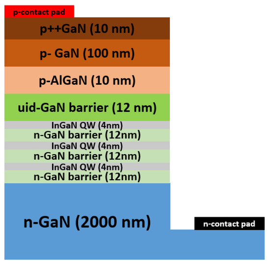
Figure 1.
Cross-sectional view of the simulated MQW LED device.
The structure is simulated from 0 to 10 V bias with a step size of 0.025 V. The same structure is simulated for six different crystal orientations, namely Ga-polar, () N-polar, nonpolar, semi-polar , semi-polar , and semi-polar , to understand the impact of crystal orientation on the LED’s modulation bandwidth.
3. Results and Discussion
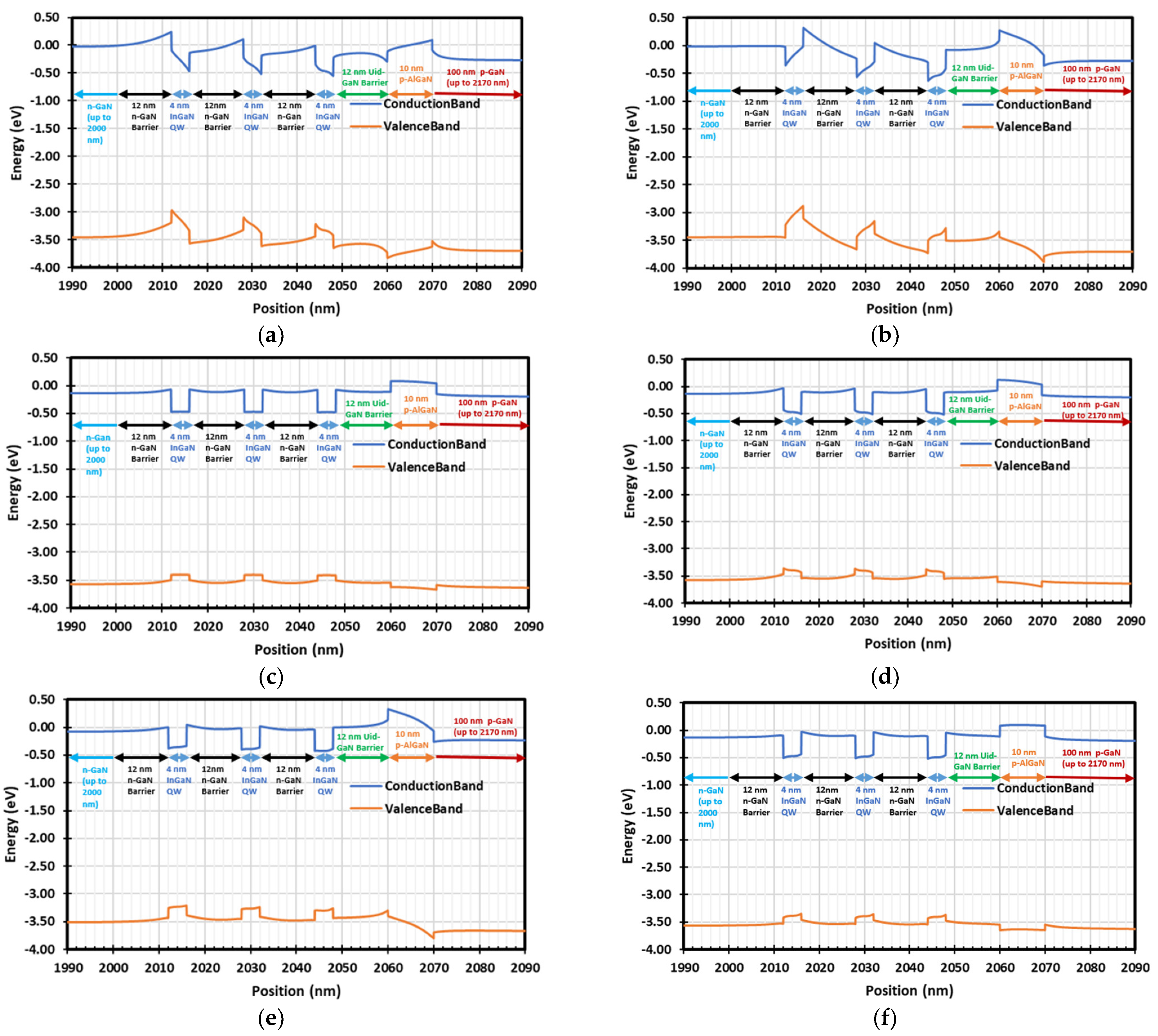
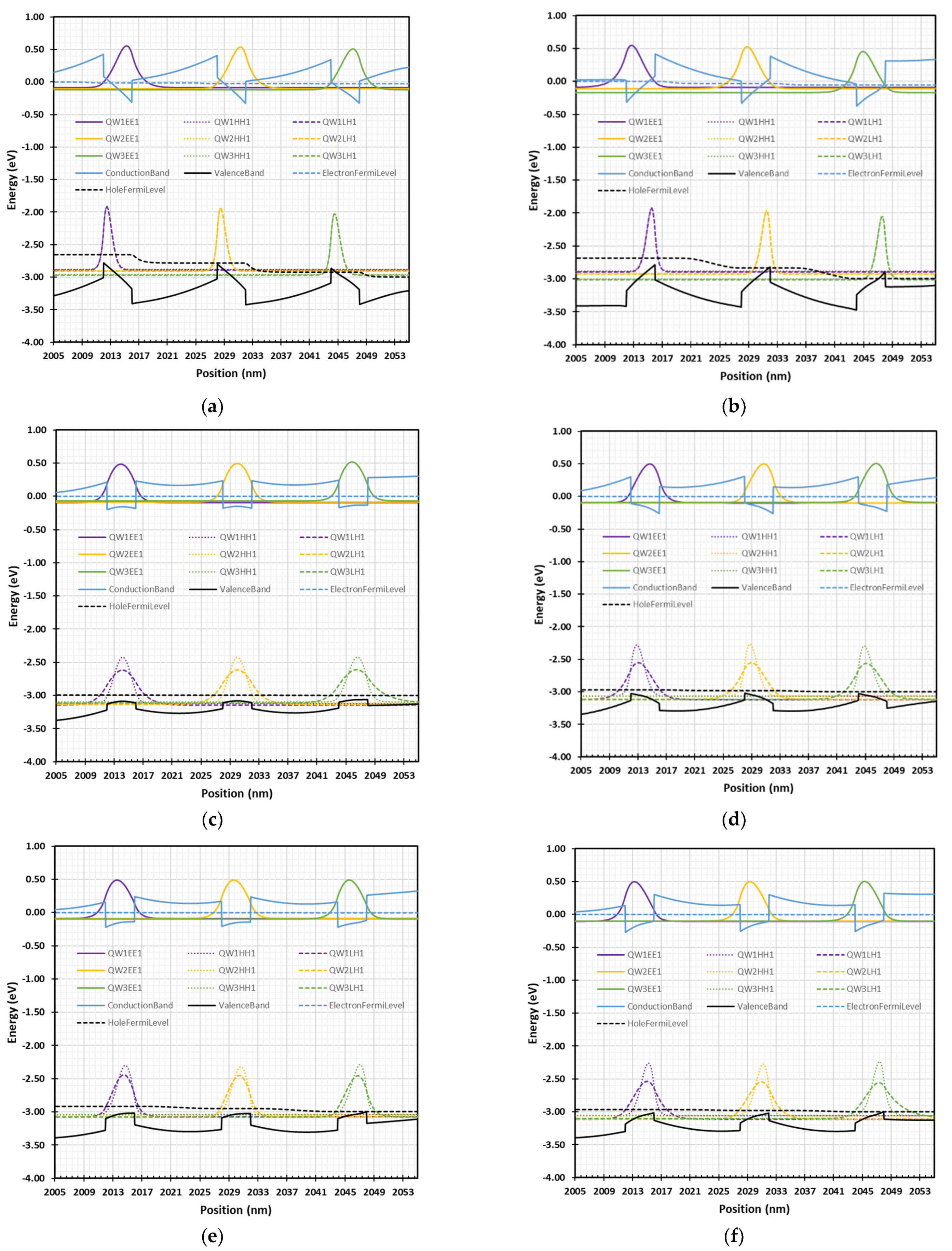
The photon generation depends on the Quantum-Confined Stark Effect (QCSE), which is hugely dependent on the crystal orientation. The band diagram of the proposed LED structure is shown in Figure 2, depicting the energy bands and the behavior of electrons and holes within the device structure. It can be seen from Figure 2 and Figure 3 that the band bending is larger for polar orientation ( Ga-polar and () N-polar) compared to the nonpolar orientation. In polar orientation, the electron and hole wave functions (Figure 3) lead to separation/displacement (and reduced overlap). Therefore, the recombination rate or efficiency is lower than nonpolar orientation. In semi-polar orientations, this effect of QCSE is in between polar and nonpolar orientations, as shown in Figure 2 and Figure 3. QCSE plays an influential role in determining the radiative recombination rates [1] and it is observed in this simulation study.
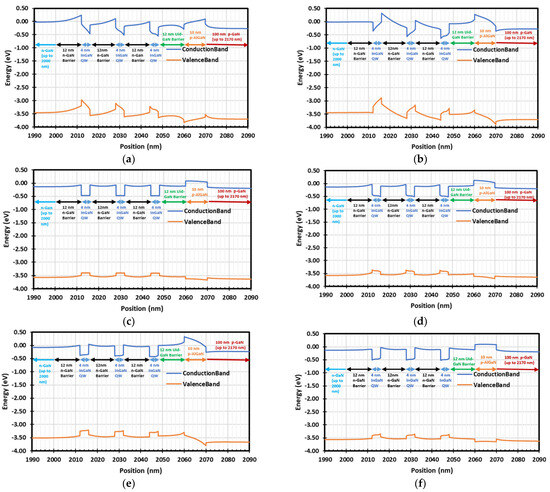
Figure 2.
Band diagram of different crystal orientations at 3.6 V bias. (a) Ga-polar. (b) () N-polar. (c) Nonpolar. (d) Semi-polar . (e) Semi-polar . (f) Semi-polar .
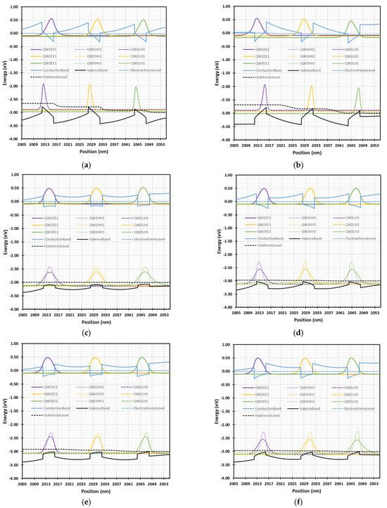
Figure 3.
Carrier wave functions of different crystal orientations at 3.6 V bias (EE, HH, and LH denote electrons, heavy holes, and light holes). (a) Ga-polar. (b) () N-polar. (c) Nonpolar. (d) Semi-polar . (e) Semi-polar . (f) Semi-polar .
Total Recombination rate R can be described as,
is the radiative recombination rate and is the non-radiative recombination rate. is the summation of and . is the non-radiative Shockley–Read–Hall (SRH) recombination that occurs due to crystal defects and dislocations in the heterostructure. is non-radiative Auger recombination which occurs at high carrier density where one electron and one hole recombine and transfer resulting energy to a third electron or hole in the high-energy band which then loses extra energy via thermal vibration.
The radiative recombination rate is expressed as,
The SRH radiative coefficient is considered as determined by previous study [24,26]. and refer to carrier concentration of electrons and holes, respectively. and represent the fermi levels of the electrons and holes, respectively. denotes the Boltzmann constant, and is the temperature.
The non-radiative Shockley–Read–Hall recombination rate () is calculated based on the Shockley–Read approach model [27] which relates the carrier lifetimes with the dislocation density. Further details of the estimation can be found in [24] and Silense Physics summary [28].
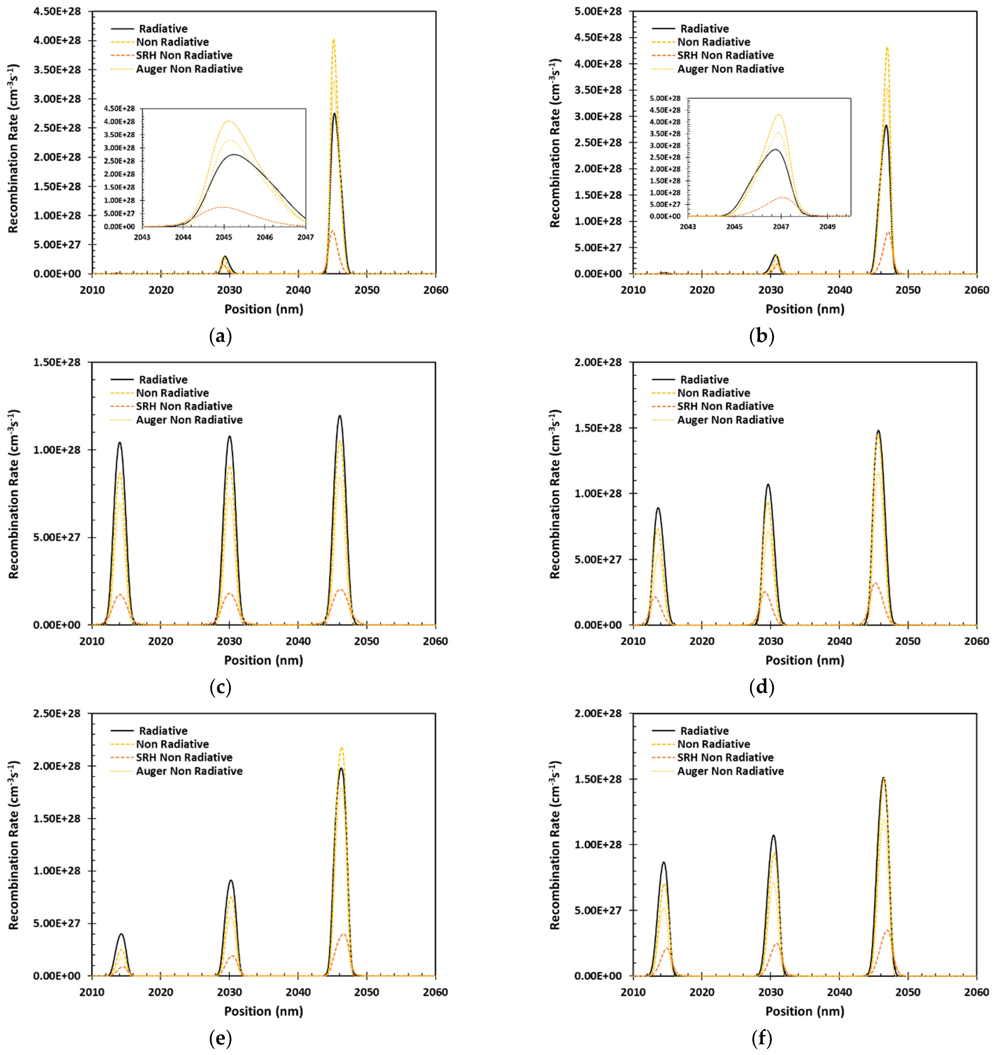
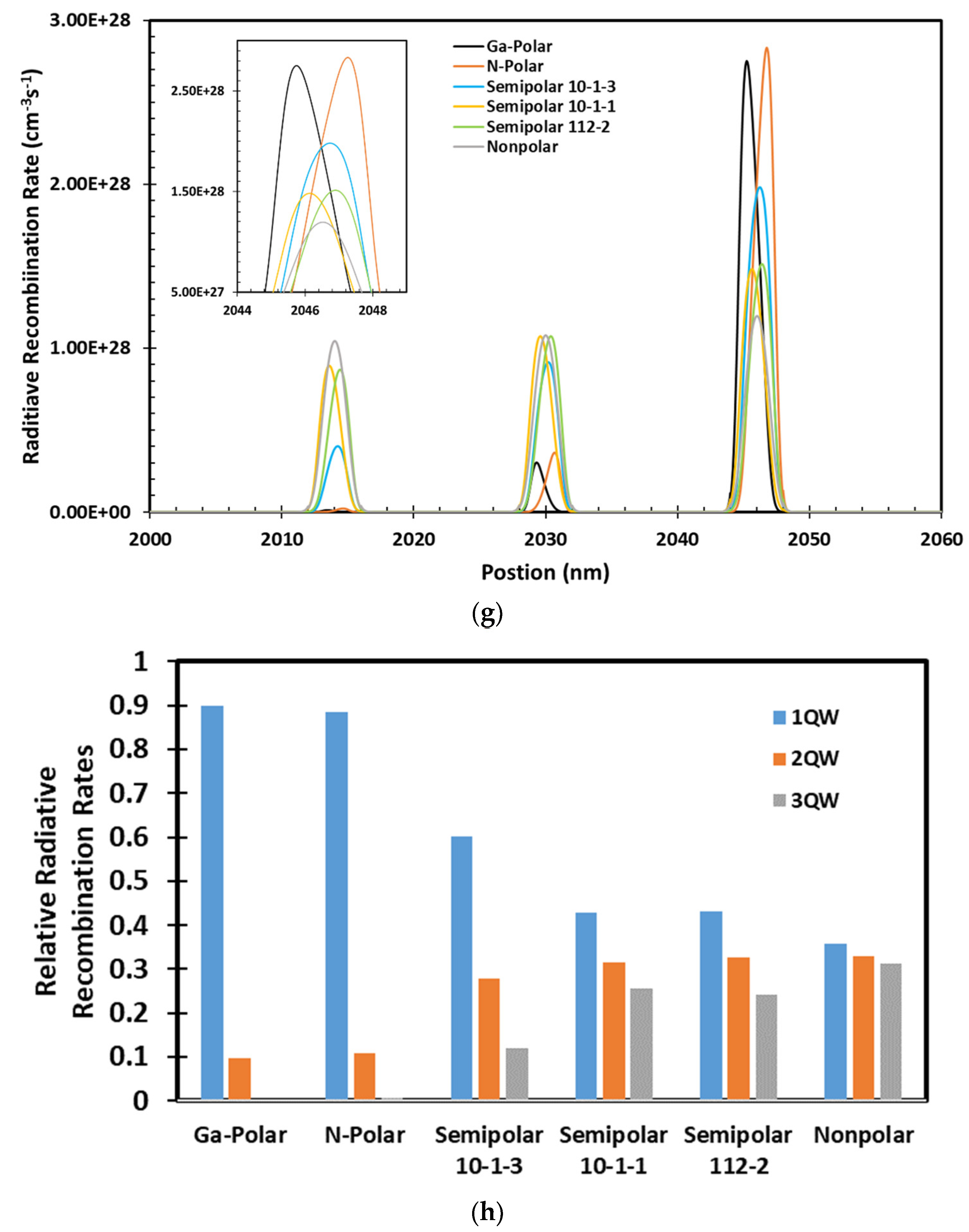
Figure 4 depicts the radiative and non-radiative recombination rates for all six simulated crystal orientations at 2 kA/cm2 current density. Non-radiative recombination rates are the summation of non-radiative Shockley–Read–Hall (SRH) recombination and non-radiative Auger recombination rates. The recombination rates are much higher in the quantum wells than in the QW barriers, so the peaks occur at the QWs. The proposed LED structures have three QWs, and the recombination peaks occur at approximately 2046 nm, 2030 nm, and 2014 nm positions (at the first QW (the one closer to p-GaN), the second QW, and the third QW). The radiative recombination is highest in N-Polar at 2 kA/cm2 current density. Most recombination occurs at first QW (the one closer to the p-GaN) at this low current density. For N-Polar and Ga-Polar orientations, approximately 90% radiative recombination occurs at the first QW, which means almost all the current is converted into recombination in the first QW. As there are higher concentrations of carriers in a particular QW that emits light, N-Polar and Ga-Polar orientations are expected to have a faster recombination rate and a higher modulation bandwidth. In the first QW, the peak radiative recombination rate for N-Polar is observed as 2.83 × 1028 cm−3s−1, whereas this value is 2.75 × 1028 cm−3s−1 in Ga-Polar and 1.98 × 1028 cm−3s−1 in semi-polar . At this current density range, N-polar orientations are expected to outperform other orientations in terms of the modulation bandwidth.
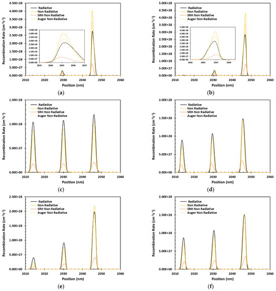
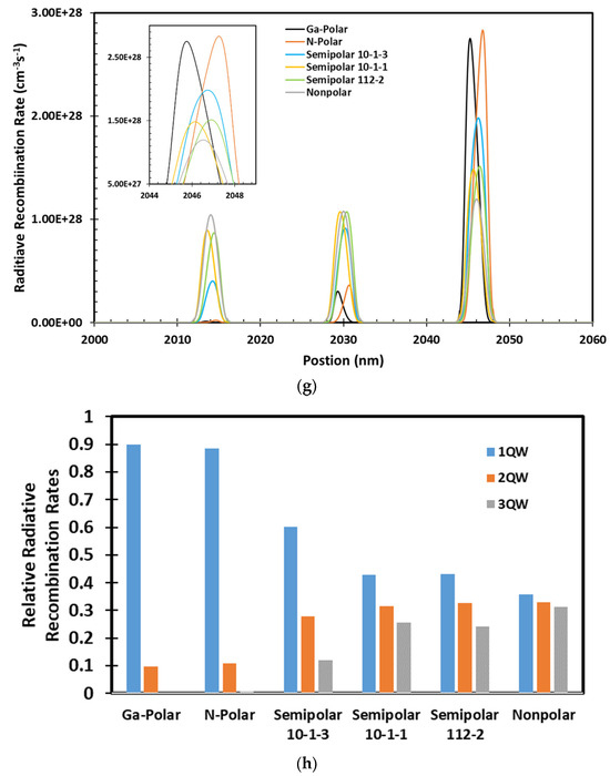
Figure 4.
Six different crystal orientation-based LEDs at 2 kA/cm2 current density: (a) Ga-polar. (b) () N-polar. (c) Nonpolar. (d) Semi-polar . (e) Semi-polar . (f) Semi-polar . (a–f): Radiative and non-radiative recombination rates; (g) radiative recombination rate at each of three QWs; (h) relative radiative recombination rates at each QWs. Note: E+n refers to 10n.
The effective differential carrier recombination lifetime is defined [29] as follows,
refers to the carrier concentration in the active region, is the Shockley–Read–Hall (SRH) non-radiative coefficient, is the SRH radiative coefficient, and is the higher-order non-radiative coefficient (Auger coefficient).
For 1D device simulation, Equation (3) can be calculated as,
where and refers to the radiative recombination rate and carrier concentration, respectively.
To integrate the recombination rate over the active region, can be expressed as,
refers to the recombination current density in the QWs. refers the electron charge (1.60 × 10⁻¹⁹ Coulombs).
refers to the Injection efficiency given by,
refers to the current density and is expressed [28] as,
and are the electron’s current density and the hole’s current density, respectively. and are the electron mobility and the hole mobility, respectively. and are the fermi levels of the electrons and holes, respectively. The electron current density and the hole current density are assumed to be proportional to the gradient of the fermi level of the electrons () and holes ), respectively. and refers to the sheet electron concentrations of the carriers in the active region and the sheet hole concentrations of the carriers in the active region, respectively.
The average carrier concentration is estimated as
Based on the above estimation, Equation (4) can be expressed as,
Equation (11) shows that the differential lifetime relies on current density (), Injection efficiency and the sheet electron and hole concentrations of the carriers in the active region ( and ). When the bias condition changes, it impacts the value of , , which in turn affects .
The modulation bandwidth of the micro-LED is dependent on the effective differential recombination lifetime (), as expressed as follows [30],
The higher the bias voltage, the higher the injected carrier concentration in the active region, resulting in a lower carrier lifetime (higher modulation bandwidth) as per Equations (3) and (12).
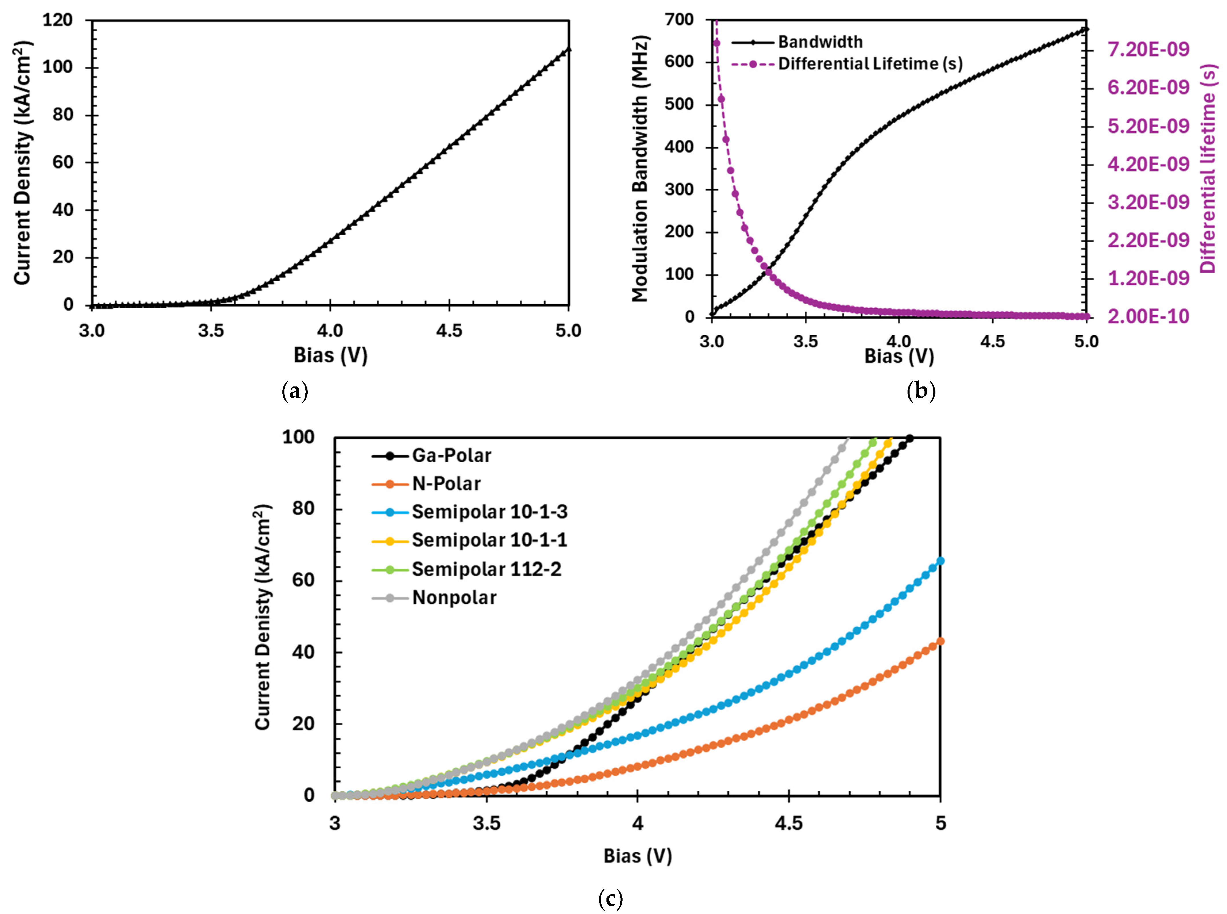
Higher bias voltage increases the active region’s carrier density, lowering the effective carrier lifetimes. It is found that the turn-on voltage is approximately 3 V. After 3 V, the structure starts to draw a high current, generating a high current density. The characteristics of current density with respect to bias voltage are presented in Figure 5a, for Ga-polar orientation as a demonstration. It can be seen the current density keeps increasing as the bias voltage increases. In this study, approximately 20 kA/cm2 current density is considered the maximum limit (this is achieved at 3.9 V biasing for this Ga-Polar orientation). Higher than this limit might cause heating issues. Figure 5b shows that the differential lifetime is reduced to 0.36 ns, resulting in a theoretical modulation bandwidth of 445 MHz (at 4 V biasing). The current densities at different bias voltages for various heterostructure orientations are plotted in Figure 5c. When the bias voltages increase, the current density increases for all crystal orientations. The current density of the Ga-polar orientation sharply increases beyond 3.6 V due to the injection of more electrons and holes into the active region compared to other crystal orientations. This behavior is caused by changes in the concentration of electrons and holes, due to polarization. The current density increases steeply after 3.6 V bias due to changes in the electron and hole quasi-Fermi levels, conduction and valence bands caused by polarization. Also, it can be observed that the current density of the Ga-polar at any bias voltage (such as 3.6 V) is not the lowest, but it exhibits the lowest performance in terms of the modulation bandwidth. This behavior of the Ga-polar is attributed to low injection efficiency and low sheet electron and hole concentrations of the carriers in the active region ( and ).
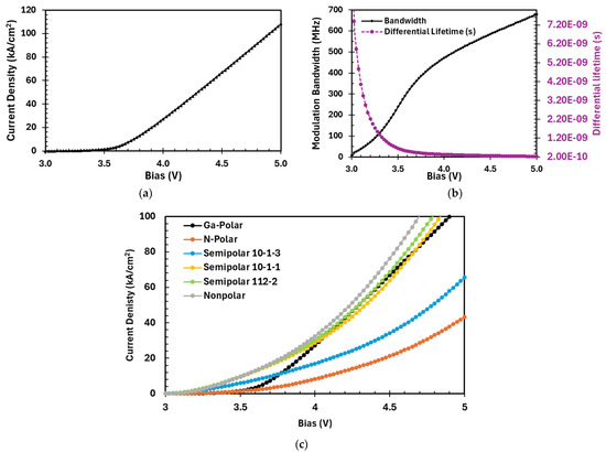
Figure 5.
(a) Ga-polar: Current density induced with respect to the bias voltage; (b) Ga-polar: Theoretical modulation bandwidth and differential carrier lifetime at different bias voltage; (c) current densities at different biases for all heterostructure orientations. Note: E-n refers to 10−n.
The maximum attainable modulation bandwidth for all six simulated orientations is shown in Figure 6. In the 0–9 kA/cm2 current density, N-polar demonstrates the highest modulation bandwidth, whereas in the range of 9–20 kA/cm2 current density, semi-polar orientation exhibits the highest modulation bandwidth. As can be seen from Table 1, with a low current density, N-Polar offers the highest modulation bandwidth compared to the semi-polar and nonpolar crystal orientations. For instance, at 2 kA/cm2, N-polar offers a modulation bandwidth of 304.6 MHz, Ga-polar offers a modulation bandwidth of 270 MHz, whereas semi-polar , semi-polar , and semi-polar , and nonpolar orientations offer a modulation bandwidth of 245.5 MHz, 237.5 MHz, 231.1 MHz, and 224.5 MHz, respectively (Figure 6b). This high offering of N-polar and Ga-polar is attributed to high carrier concentration in one particular single QW which causes a shorter carrier lifetime than the simulated orientations. In the 0–9 kA/cm2 current density range, most of the light is emitted from the first QW (the one closer to the p-GaN). For instance, at 2 kA/cm2 current density, more than 88% of radiative recombination occurs at the first QW of the N-Polar structure, and the injection efficiency is observed as high as 0.99. Therefore, almost all the injected electron (current) is converted into recombination in the first QW. As there are higher concentrations of carriers in the first QW (which is emitting light), N-Polar orientation demonstrates the highest radiative recombination rate of 2.83 × 1028 cm−3s−1 and the highest modulation bandwidth of 304.6 MHz compared to the other five orientations. Also, N-polar orientation is performing the best, attributing to a higher ratio of radiative to auger recombination coefficients. For instance, in the first quantum well (the one closer to the p-type), the radiative recombination rate of N-polar orientation is found as 2.83 × 1028 cm−3s−1, whereas in the Ga-polar, semi-polar and nonpolar the radiative recombination rates are recorded as 2.75 × 1028 cm−3s−1, 1.98 × 1028 cm−3s−1, and 1.20 × 1028 cm−3s−1, assisting N-polar to perform better.
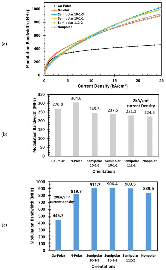
Figure 6.
Modulation bandwidth of different crystal orientation-based LEDs: (a) in 0–25 kA/cm2 current density range, (b) at 2 kA/cm2 current density, and (c) at 20 kA/cm2 current density.

Table 1.
Comparison of radiative recombination rates occurring at each quantum well (QW) under various applied current densities. Injection efficiency and modulation bandwidth are also provided.
In the 0–3 kA/cm2 current density, Ga-Polar offers the second-highest modulation bandwidth as it demonstrates the second-lowest carrier lifetime due to the second-highest recombination rate among these six simulated structures. For instance, at 2 kA/cm2 current density, Ga-Polar exhibits a radiative recombination rate of 2.75 × 1028 cm−3s−1 and a modulation bandwidth of 270 MHz (second highest). This behavior is attributed to having 90% of total electron injection (due to current) being converted into recombination in the first QW and also having 0.91 injection efficiency at 2 kA/cm2 current density.
In the 0–9 kA/cm2 current density range, for four other crystal orientations simulated in this study (except N-Polar and Ga-Polar), the injected current is distributed well among all three QWs. For instance, at 2 kA/cm2 current density, the radiative recombination ratio in 1st QW:2nd QW:3rd QW are as follows: semi-polar (60.15:27.82:12.03), semi-polar (42.86:31.43:25.71), semi-polar (43.06:32.64:24.31) and nonpolar (35.82:32.84:31.34). This implies that the recombinations happening per QW for these four crystal orientations are approximately 3-fold lower than N-Polar and Ga-Polar. Due to lower carrier concentration per QW at a low current density of 2 kA/cm2, these four crystal orientations show slower recombination rates and smaller modulation bandwidths. Note that, in the 0–3 kA/cm2 current density range, the non-polar depicts the lowest modulation bandwidth due to a lower injection efficiency than other semi-polar orientations as shown in Table 1.
When the current density is in the range of 3–20 kA/cm2, Ga-polar exhibits the lowest modulation bandwidth owing to decreased injection efficiency. Above 3 kA/cm2 current density, the injection efficiency decreased dramatically (drops from 0.9 to 0.3 at 3 kA/cm2 to 20 kA/cm2) compared to other crystal structures, so the injected electron (current) converted into the recombination is lower. Thus, the recombination lifetime is longer, resulting in a lower bandwidth. Owing to the low injection efficiency, the Ga-Polar orientation LED offers a low modulation bandwidth of 445.7 MHz at a high current density of 20 kA/cm2. It indicates that the ratio of the current density converted to the recombination rates from the QW layers to the total current density is much lower, which may limit the running of the Ga-polar at such a high current.
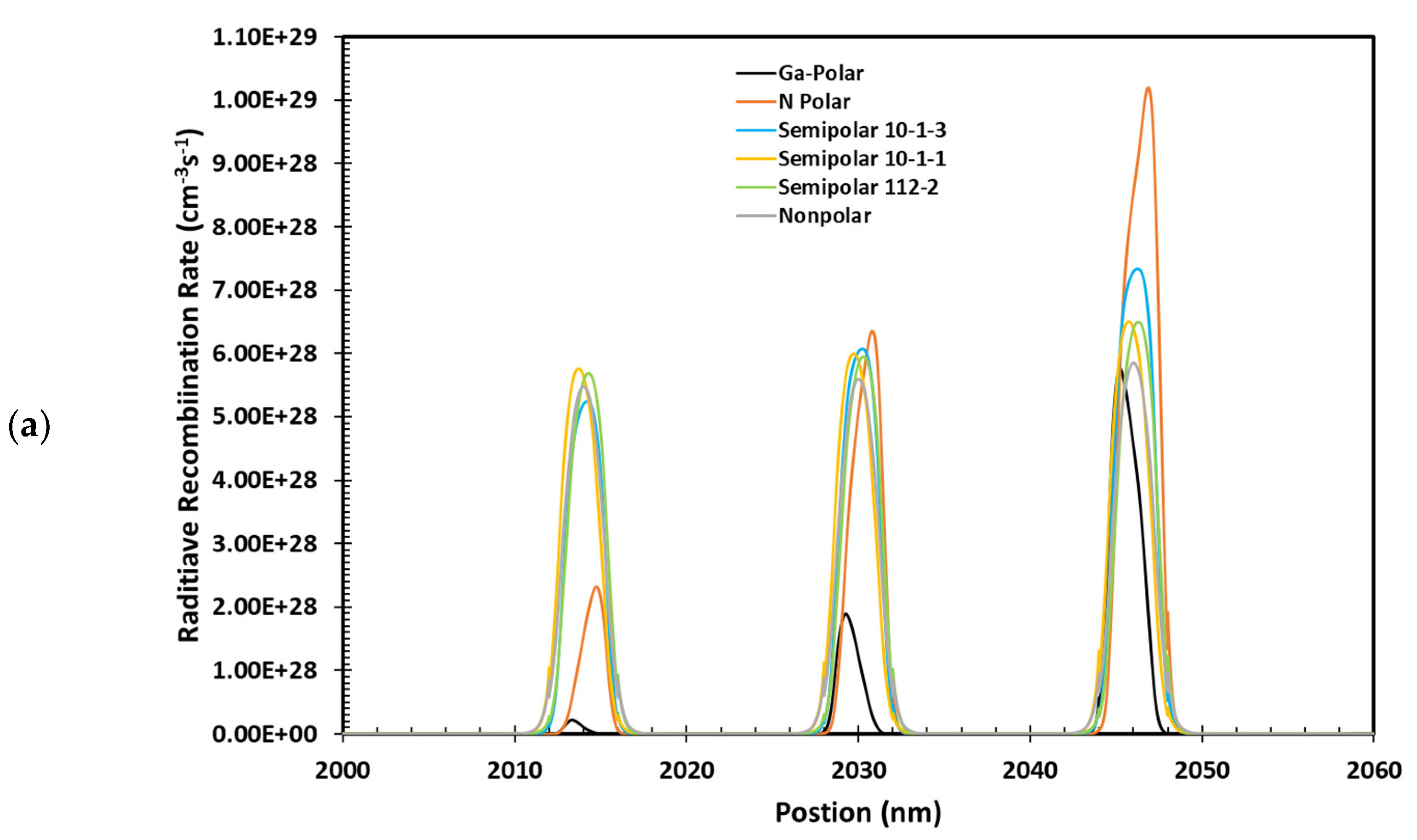
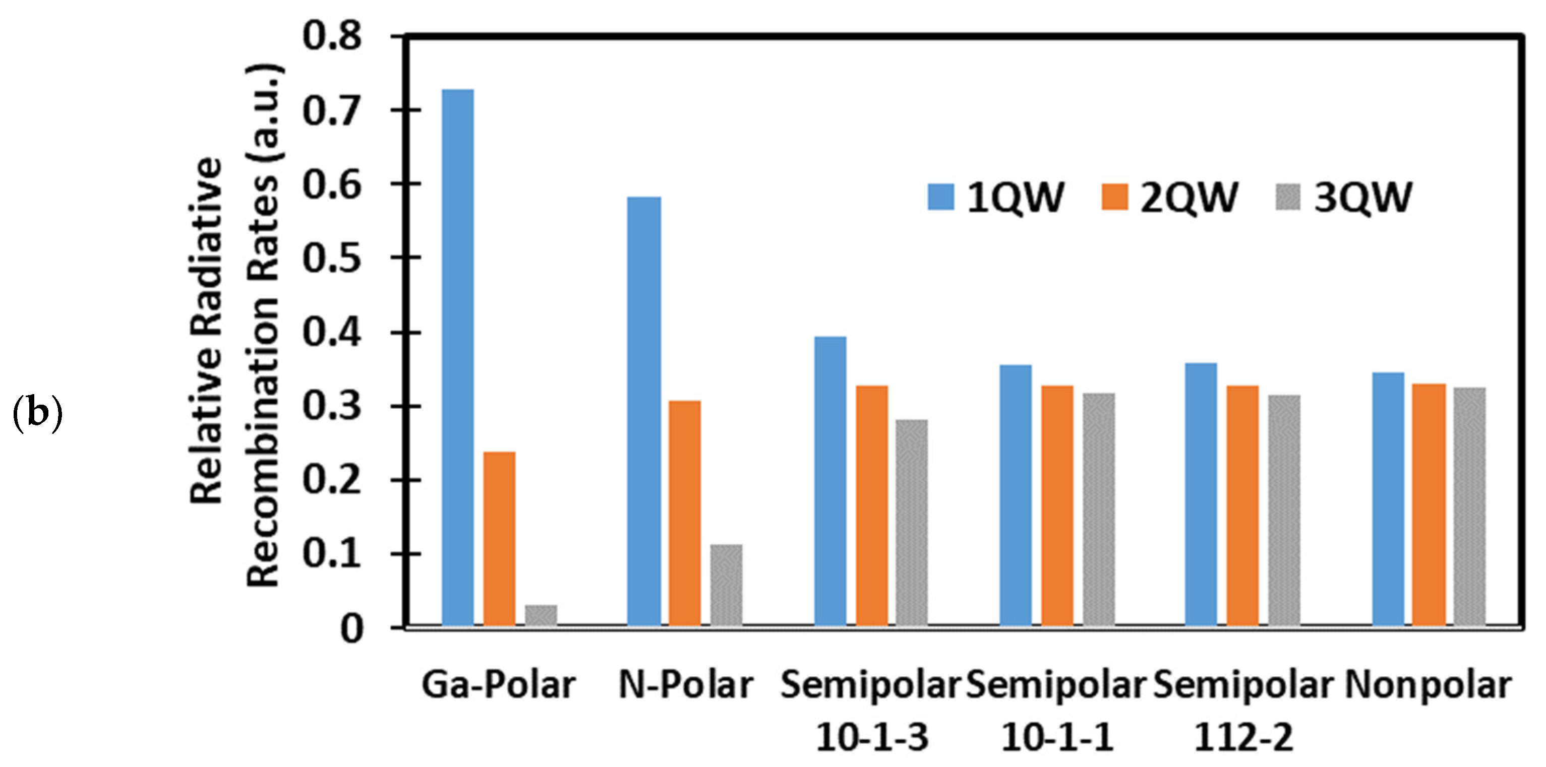
As shown in Table 1 and Figure 6, when subjected to high current density (9–20 kA/cm2), semi-polar offers the highest modulation bandwidth compared to the Polar and nonpolar crystal orientations. For instance, at 20 kA/cm2, semi-polar offers a modulation bandwidth of 912.7 MHz, which is higher than semi-polar , semi-polar , nonpolar, N-polar, and Ga-Polar orientations that offer a modulation bandwidth of 906.4 MHz, 903.5 MHz, 839.6 MHz, 819.7 MHz, and 445.7 MHz, respectively (see Figure 6c). This high offering of semi-polar and nonpolar orientation is attributed to the larger wave-function overlap and shorter carrier lifetime than the polar structure. Semi-polar orientation performs better owing to a higher ratio of radiative to auger recombination coefficients [10]. For instance, in the first quantum well (the one closer to the p-type), the radiative recombination rates of semi-polar is found as 7.33 × 1028 cm−3s−1 while for semi-polar , semi-polar , nonpolar, N-polar and Ga-Polar orientations nonpolar orientations it is observed as 6.5 × 1028 cm−3s−1, 6.5 × 1028 cm−3s−1, 5.85 × 1028 cm−3s−1, 1.02 × 1029 cm−3s−1, and 5.76 × 1028 cm−3s−1, respectively, which allows semi-polar 2 to perform better. At high current density, the injected electrons (current) are distributed to all three QWs as the number of carriers and carrier concentrations are very high. The current is converted into recombination in all three QWs. The carrier concentration is almost homogeneously distributed for all three semi-polar and nonpolar orientations at 20 kA/cm2 current density. In the first, second and third QWs, the radiative recombination ratios are as follows: semi-polar (39.30:32.62:28.07), semi-polar (35.52:32.79:31.69), semi-polar (35.81:32.78:31.40) and nonpolar (34.51:33.04:32.45), as depicted in Figure 7. As the carrier concentration is already high at 20 kA/cm2 current density and the carriers are distributed almost equally, and the semi-polar and nonpolar orientations demonstrate a better modulation bandwidth. It is worth noting that in the Ga-polar orientation, approximately 72% of total recombination occurs in the first quantum well. One might assume that this would result in a high modulation bandwidth. However, in reality, the modulation bandwidth for Ga-Polar is the lowest (445.7 MHz) at 20 kA/cm2 current density due to a very low injection efficiency of only 0.3 and low sheet electron and hole concentrations of the carriers in the active region. Table 2 shows the percentage of radiative recombination rates at a particular QW under two different current densities (2 kA/cm2 and 20 kA/cm2). In 20 kA/cm2 current density, N-polar offers as high as 819 MHz owing to carrier concentrations distributed into each of the three QWs and higher injection efficiency. Note that at high current density, there are large no. of carriers available to be distributed to each of three QWs, and all three QWs are contributing to a lower radiative lifetime, resulting in a high modulation bandwidth. Also, the injection efficiency of N-polar is as high as 0.92, enabling it to offer a high modulation bandwidth of 819.7 at 20 kA/cm2 current density. The efficiency droop is calculated for all six simulated orientation LED structures by comparing the result attained at low current density (i.e., 2 kA/cm2) and high current density (i.e., 20 kA/cm2). The efficiency droop for Ga-polar, N-polar, semi-polar , semi-polar , semi-polar , and nonpolar LEDs are observed as 70%, 26%, 28%, 32%, 32%, and 37%, respectively. Based on this result, it is obvious that semi-polar orientation LED heterostructure is the optimum choice as it offers the highest modulation bandwidth of 912.7 MHz and a high injection efficiency of 97%, a low efficiency droop of 28%.

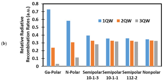
Figure 7.
At 20 kA/cm2 current density: (a) radiative recombination rate at each of three QWs; (b) relative radiative recombination rates at each QWs. Note: E+n refers to 10n.

Table 2.
Percentage of the radiative recombination rates at a particular QW at two different current density.
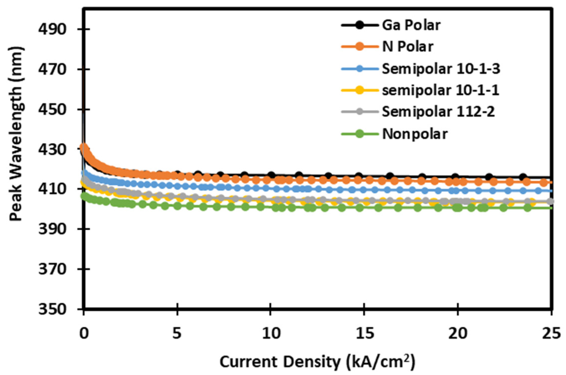
A comparison plot is given in Figure 8, where total light emissions for all crystal orientations are compared at 20 kA/cm2 current density. In all simulated orientations, the emission is in the blue region with the following values—semi-polar occurs at 409 nm wavelength with a peak emission intensity of 1.54 × 1021 cm−2s−1nm−1, semi-polar occurs at 403 nm wavelength with a peak emission intensity of 1.5 × 1021 cm−2s−1nm−1, semi-polar 2 occurs at 404 nm wavelength with a peak emission intensity of 1.48 × 1021 cm−2s−1nm−1, nonpolar occurs at 400 nm wavelength with a peak emission intensity of 1.47 × 1021 cm−2s−1nm−1, N-polar occurs at 413 nm wavelength with a peak emission intensity of 1.2 × 1021 cm−2s−1nm−1, and Ga-polar occurs at 416 nm wavelength with a peak emission intensity of 5.02 × 1020 cm−2s−1nm−1. The semi-polar orientation outperforms the other orientations owing to a higher radiative combination and less QCSE effect. Figure 9 depicts the peak emission wavelength of different crystal orientation-based LEDs in the 0–25 kA/cm2 current density range. The peak emission wavelength remained stable for all six simulated crystal orientations, indicating the color stability of the LEDs. The peak emission wavelength for each orientation is between 400 nm and 430 nm, with a slight blue shift observed as the current density increased.
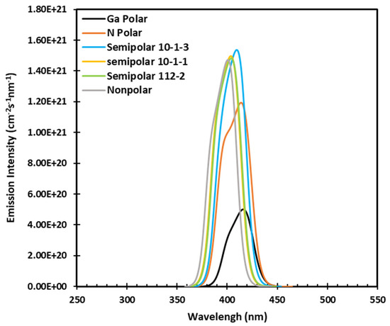
Figure 8.
Total emission intensity from each heterostructure at 20 kA/cm2 current density. Note: E+n, refers to 10n.
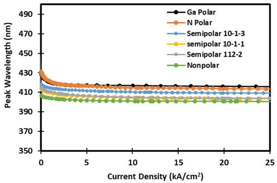
Figure 9.
Peak emission wavelength of different crystal orientation-based LEDs in 0–25 kA/cm2 current density range.
According to the results obtained in this study, the semi-polar is observed as the best orientation to attaining a high modulation bandwidth and has the potential to support a high-speed visible light communication system. It demonstrated a modulation bandwidth of over 912 MHz for semi-polar orientation, at 20 kA/cm2 current density, whereas semi-polar and semi-polar orientation LEDs have demonstrated a modulation bandwidth of approximately 905 MHz, indicating significant potential. For the semi-polar case, this study obtained a modulation bandwidth of more than 912 MHz at 20 kA/cm2, whereas the study in [10] observed 325 MHz at 1 kA/cm2 current density. The nonpolar orientation LED demonstrated an approximately 840 MHz modulation bandwidth at 20 kA/cm2 current density, whereas previous work [16] reported 525 MHz. This simulation demonstrated a 400 MHz modulation bandwidth for Ga-polar cases at 20 kA/cm2 current density. Previous works have shown 230 MHz [31] and 123 MHz at 1 kA/cm2 [10] for polar samples. Significant advancements have been made in developing high-performance nonpolar, semi-polar, and polar GaN devices [14]. Researchers demonstrated some artificial semi-polar planes such as 1 and , by employing precise growth conditions and specific patterning techniques on sapphire substrates, showing great promise [32]. Researchers have successfully grown single-phase nonpolar m-plane GaN [33] on planar bulk m-plane GaN substrate and nonpolar a-plane [34] GaN thin films on r-plane sapphire. Furthermore, different orientations, including semi-polar () were achieved on m-plane [35] and a-plane [36] GaN SiC substrates. Semi-polar () [37] and nonpolar m-plane were also obtained in Si substrates [38], by implementing patterned v-grooves on Si (001) and (112) [39]. It is believed that affordable and large area nonpolar and semi-polar substrates production would be possible in the near future to meet the visible light communication industry demands. Our study will guide the epitaxy experts towards optimizing LED structure growth on nonpolar and semi-polar substrate orientations. The proposed semipolar and nonpolar-based LEDs have the potential to be used as transmitters for high-speed visible light communication system applications like high-speed wireless communication in the office and home, where 4 K video streaming and larger file transfers are crucial. Moreover, these LEDs can be used for Augmented Reality (AR), Virtual Reality (VR), and industrial automation for 5G-and-beyond connectivity towards Gbps-speed visible light communication.
4. Conclusions
In this study, planar chip structure has been simulated to demonstrate how different crystal orientations impact an LED’s recombination rates and the modulation bandwidth. Among six different simulated orientations, semi-polar LED demonstrated the highest modulation bandwidth owing to the higher radiative combination and reduced QCSE effect. At a current density of 20 kA/cm2, semi-polar offers a modulation bandwidth of 912.7 MHz. This finding demonstrates that semi-polar MQW LED shows the potential for high-speed visible light communications. We believe this study will develop an understanding of and encourage further studies on the different crystal orientations of GaN to enable high-speed LED transmitters towards high-speed visible light communications.
Author Contributions
M.J.F., conceptualization, methodology, data curation, and manuscript writing; K.B., methodology and manuscript revision. N.K., manuscript revision, project resources and administration, and supervision. All authors have read and agreed to the published version of the manuscript.
Funding
This research received no external funding.
Institutional Review Board Statement
Not applicable.
Informed Consent Statement
Not applicable.
Data Availability Statement
The data supporting this study’s findings are available from the corresponding author upon reasonable request. The request should be made via email.
Acknowledgments
The authors wish to acknowledge the Department of Electrical & Computer System Engineering, Monash University, for funding this study and Kirill Bulashevich from the STR group for technical support and discussion.
Conflicts of Interest
The authors declare that they have no known competing financial interests or personal relationships that could have appeared to influence the work reported in this paper.
References
- Rajbhandari, S.; McKendry, J.J.; Herrnsdorf, J.; Chun, H.; Faulkner, G.; Haas, H.; Watson, I.M.; O’Brien, D.; Dawson, M.D. A review of gallium nitride LEDs for multi-gigabit-per-second visible light data communications. Semicond. Sci. Technol. 2017, 32, 023001. [Google Scholar] [CrossRef]
- Muhammad, U.; Nawaz, N.; Saba, K.; Karimov, K.; Muhammad, N. Experimental and numerical analysis of the indium-content on the internal electromechanical field in GaN-based light-emitting diodes. Optik 2018, 172, 1193–1198. [Google Scholar] [CrossRef]
- Zafar, F.; Bakaul, M.; Parthiban, R. Laser-diode-based visible light communication: Toward gigabit class communication. IEEE Commun. Mag. 2017, 55, 144–151. [Google Scholar] [CrossRef]
- Xiao, H.; Xiao, X.; Wu, D.; Wang, R.; Wang, K.; Chiang, K.S. Effects of injection current on the modulation bandwidths of quantum-dot light-emitting diodes. IEEE Trans. Electron Devices 2019, 66, 4805–4810. [Google Scholar] [CrossRef]
- Shi, J.-W.; Huang, H.-Y.; Sheu, J.-K.; Chen, C.-H.; Wu, Y.-S.; Lai, W.-C. The improvement in modulation speed of GaN-based Green light-emitting diode (LED) by use of n-type barrier doping for plastic optical fiber (POF) communication. IEEE Photonics Technol. Lett. 2006, 18, 1636–1638. [Google Scholar] [CrossRef]
- James Singh, K.; Huang, Y.-M.; Ahmed, T.; Liu, A.-C.; Huang Chen, S.-W.; Liou, F.-J.; Wu, T.; Lin, C.-C.; Chow, C.-W.; Lin, G.-R. Micro-LED as a promising candidate for high-speed visible light communication. Appl. Sci. 2020, 10, 7384. [Google Scholar] [CrossRef]
- Xie, E.; He, X.; Islim, M.S.; Purwita, A.A.; McKendry, J.J.; Gu, E.; Haas, H.; Dawson, M.D. High-speed visible light communication based on a III-nitride series-biased micro-LED array. J. Light. Technol. 2019, 37, 1180–1186. [Google Scholar] [CrossRef]
- McKendry, J.J.; Massoubre, D.; Zhang, S.; Rae, B.R.; Green, R.P.; Gu, E.; Henderson, R.K.; Kelly, A.; Dawson, M.D. Visible-light communications using a CMOS-controlled micro-light-emitting-diode array. J. Light. Technol. 2011, 30, 61–67. [Google Scholar] [CrossRef]
- Maaskant, P.P.; Shams, H.; Akhter, M.; Henry, W.; Kappers, M.J.; Zhu, D.; Humphreys, C.J.; Corbett, B. High-speed substrate-emitting micro-light-emitting diodes for applications requiring high radiance. Appl. Phys. Express 2013, 6, 022102. [Google Scholar] [CrossRef]
- Monavarian, M.; Rashidi, A.; Aragon, A.; Oh, S.; Rishinaramangalam, A.; DenBaars, S.; Feezell, D. Impact of crystal orientation on the modulation bandwidth of InGaN/GaN light-emitting diodes. Appl. Phys. Lett. 2018, 112, 041104. [Google Scholar] [CrossRef]
- Monavarian, M.; Rashidi, A.; Aragon, A.; Nami, M.; Oh, S.; DenBaars, S.; Feezell, D. Trade-off between bandwidth and efficiency in semipolar (20 2¯ 1¯) InGaN/GaN single-and multiple-quantum-well light-emitting diodes. Appl. Phys. Lett. 2018, 112, 191102. [Google Scholar] [CrossRef]
- Zhu, D.; Humphreys, C.J. Solid-state lighting based on light emitting diode technology. Opt. Our Time 2016, 87–118. [Google Scholar] [CrossRef]
- Tabbakh, T.A.; Anandan, D.; Sheldon, M.J.; Tyagi, P.; Alfaifi, A. Recent Advancements in GaN LED Technology. In Light-Emitting Diodes-New Perspectives; IntechOpen: London, UK, 2022. [Google Scholar]
- Monavarian, M.; Rashidi, A.; Feezell, D. A Decade of Nonpolar and Semipolar III-Nitrides: A Review of Successes and Challenges. Phys. Status Solidi (a) 2019, 216, 1800628. [Google Scholar] [CrossRef]
- Romanov, A.; Baker, T.; Nakamura, S.; Speck, J. Strain-induced polarization in wurtzite III-nitride semipolar layers. J. Appl. Phys. 2006, 100, 023522. [Google Scholar] [CrossRef]
- Rashidi, A.; Monavarian, M.; Aragon, A.; Okur, S.; Nami, M.; Rishinaramangalam, A.; Mishkat-Ul-Masabih, S.; Feezell, D. High-speed nonpolar InGaN/GaN LEDs for visible-light communication. IEEE Photonics Technol. Lett. 2017, 29, 381–384. [Google Scholar] [CrossRef]
- Xie, E.; Stonehouse, M.; Ferreira, R.; McKendry, J.J.; Herrnsdorf, J.; He, X.; Rajbhandari, S.; Chun, H.; Jalajakumari, A.V.; Almer, O. Design, fabrication, and application of GaN-based micro-LED arrays with individual addressing by N-electrodes. IEEE Photonics J. 2017, 9, 1–11. [Google Scholar] [CrossRef]
- Xu, F.; Qiu, P.; Tao, T.; Tian, P.; Liu, X.; Zhi, T.; Xie, Z.; Liu, B.; Zhang, R. High Bandwidth Semi-Polar InGaN/GaN Micro-LEDs With Low Current Injection for Visible Light Communication. IEEE Photonics J. 2023, 15, 1–4. [Google Scholar] [CrossRef]
- Chai, H.; Yao, S.; Lei, L.; Zhu, Z.; Li, G.; Wang, W. High-speed parallel micro-LED arrays on Si substrates based on via-holes structure for visible light communication. IEEE Electron. Device Lett. 2022, 43, 1279–1282. [Google Scholar] [CrossRef]
- Zhu, S.; Shan, X.; Qiu, P.; Wang, Z.; Yuan, Z.; Cui, X.; Zhang, G.; Tian, P. Low-power high-bandwidth non-polar InGaN micro-LEDs at low current densities for energy-efficient visible light communication. IEEE Photonics J. 2022, 14, 1–5. [Google Scholar] [CrossRef]
- Schubert, E.F. Light-Emitting Diodes, 2nd ed.; Cambridge University Press: Cambridge, UK, 2003; p. 88. [Google Scholar]
- Konoplev, S.S.; Bulashevich, K.A.; Karpov, S.Y. From large-size to micro-LEDs: Scaling trends revealed by modeling. Phys. Status Solidi (a) 2018, 215, 1700508. [Google Scholar] [CrossRef]
- Bulashevich, K.; Karpov, S.Y. Is Auger recombination responsible for the efficiency rollover in III-nitride light-emitting diodes? Phys. Status Solidi c 2008, 5, 2066–2069. [Google Scholar] [CrossRef]
- Karpov, S.Y.; Makarov, Y.N. Dislocation effect on light emission efficiency in gallium nitride. Appl. Phys. Lett. 2002, 81, 4721–4723. [Google Scholar] [CrossRef]
- Bandić, Z.; Bridger, P.; Piquette, E.; McGill, T. The values of minority carrier diffusion lengths and lifetimes in GaN and their implications for bipolar devices. Solid-State Electron. 2000, 44, 221–228. [Google Scholar] [CrossRef]
- Im, J.; Moritz, A.; Steuber, F.; Härle, V.; Scholz, F.; Hangleiter, A. Radiative carrier lifetime, momentum matrix element, and hole effective mass in GaN. Appl. Phys. Lett. 1997, 70, 631–633. [Google Scholar] [CrossRef]
- Shockley, W.; Read Jr, W. Statistics of the recombinations of holes and electrons. Phys. Rev. 1952, 87, 835. [Google Scholar] [CrossRef]
- STR-Soft. Silense Physics Summary. Available online: https://str-soft.com/devices/silense/ (accessed on 1 November 2023).
- Green, R.P.; McKendry, J.J.; Massoubre, D.; Gu, E.; Dawson, M.D.; Kelly, A.E. Modulation bandwidth studies of recombination processes in blue and green InGaN quantum well micro-light-emitting diodes. Appl. Phys. Lett. 2013, 102, 091103. [Google Scholar] [CrossRef]
- Lan, H.-Y.; Tseng, I.-C.; Kao, H.-Y.; Lin, Y.-H.; Lin, G.-R.; Wu, C.-H. 752-MHz Modulation Bandwidth of High-Speed Blue Micro Light-Emitting Diodes. IEEE J. Quantum Electron. 2018, 54, 1–6. [Google Scholar] [CrossRef]
- Liu, X.; Tian, P.; Wei, Z.; Yi, S.; Huang, Y.; Zhou, X.; Qiu, Z.-J.; Hu, L.; Fang, Z.; Cong, C. Gbps long-distance real-time visible light communications using a high-bandwidth GaN-based micro-LED. IEEE Photonics J. 2017, 9, 1–9. [Google Scholar] [CrossRef]
- Leung, B.; Wang, D.; Kuo, Y.S.; Han, J. Complete orientational access for semipolar GaN devices on sapphire. Phys. Status Solidi (b) 2016, 253, 23–35. [Google Scholar] [CrossRef]
- Kim, K.C.; Schmidt, M.C.; Sato, H.; Wu, F.; Fellows, N.; Saito, M.; Fujito, K.; Speck, J.S.; Nakamura, S.; DenBaars, S.P. Improved electroluminescence on nonpolar m-plane InGaN/GaN quantum wells LEDs. Phys. Status Solidi (RRL)–Rapid Res. Lett. 2007, 1, 125–127. [Google Scholar] [CrossRef]
- Craven, M.; Lim, S.; Wu, F.; Speck, J.; DenBaars, S. Structural characterization of nonpolar (1120) a-plane GaN thin films grown on (1102) r-plane sapphire. Appl. Phys. Lett. 2002, 81, 469–471. [Google Scholar] [CrossRef]
- Cho, Y.; Sun, Q.; Lee, I.-H.; Ko, T.-S.; Yerino, C.; Han, J.; Kong, B.; Cho, H.; Wang, S. Reduction of stacking fault density in m-plane GaN grown on SiC. Appl. Phys. Lett. 2008, 93, 111904. [Google Scholar] [CrossRef]
- Craven, M.; Wu, F.; Chakraborty, A.; Imer, B.; Mishra, U.; DenBaars, S.; Speck, J. Microstructural evolution of a-plane GaN grown on a-plane SiC by metalorganic chemical vapor deposition. Appl. Phys. Lett. 2004, 84, 1281–1283. [Google Scholar] [CrossRef]
- Izyumskaya, N.; Zhang, F.; Okur, S.; Selden, T.; Avrutin, V.; Özgür, Ü.; Metzner, S.; Karbaum, C.; Bertram, F.; Christen, J. Optical studies of strain and defect distribution in semipolar (11 01) GaN on patterned Si substrates. J. Appl. Phys. 2013, 114, 113502. [Google Scholar] [CrossRef]
- Ding, K.; Avrutin, V.; Izyumskaya, N.; Metzner, S.; Bertram, F.; Christen, J.; Ozgur, U.; Morkoc, H. Recent progress in nonpolar and semi-polar GaN light emitters on patterned Si substrates. Gallium Nitride Mater. Devices XIII 2018, 10532, 6–21. [Google Scholar]
- Izyumskaya, N.; Okur, S.; Zhang, F.; Monavarian, M.; Avrutin, V.; Özgür, Ü.; Metzner, S.; Karbaum, C.; Bertram, F.; Christen, J. Optical properties of m-plane GaN grown on patterned Si (112) substrates by MOCVD using a two-step approach. In Gallium Nitride Materials and Devices IX; SPIE: San Francisco, CA, USA, 2014; pp. 257–263. [Google Scholar]
Disclaimer/Publisher’s Note: The statements, opinions and data contained in all publications are solely those of the individual author(s) and contributor(s) and not of MDPI and/or the editor(s). MDPI and/or the editor(s) disclaim responsibility for any injury to people or property resulting from any ideas, methods, instructions or products referred to in the content. |
© 2024 by the authors. Licensee MDPI, Basel, Switzerland. This article is an open access article distributed under the terms and conditions of the Creative Commons Attribution (CC BY) license (https://creativecommons.org/licenses/by/4.0/).


