Abstract
Spectroscopic ellipsometry (SE) is an effective method to measure the optical constants of thin film materials which is very sensitive to the surface topography of thin films. When performing ellipsometric measurements of the optical constants of solid materials with rough surfaces, the equivalent medium approximation (EMA) model is often used to characterize the surface topography. The EMA model is determined by two parameters of equivalent thickness dEMA and the void volume fraction f. In most applications, the void volume fraction parameter f is always set to an empirical 50% without any instructions, and then the thickness parameter dEMA is determined by fitting. In order to improve the accuracy of the fitting results, it is necessary to validate the construction law of the EMA model in the ellipsometry analysis considering characteristic parameters of the actual surface topography. In this paper, the influence of the surface topographical parameters on EMA model is analyzed. The method of FDTD (finite difference time domain) is employed to simulate the SiO2 films with different topographical parameters and EMA model are carried out on these samples. The analysis results show that the EMA model constructed with dEMA = σ + 0.80 h (σ: the root mean square height, h: the average height) can better fit the SE parameters. The proposed method can facilitate a better understanding and utilization of the EMA model in SE application.
1. Introduction
Spectroscopic ellipsometry (SE) is a surface sensitive characterization technique used to investigate material properties, for example, film thickness and optical properties. SE has been widely applied in many fields, such as physics, chemistry, material science and microelectronics. For high precision characterization, SE based on precise model solution has a strict requirement for thin film surface quality. However, thin film material often exhibits an unavoidable rough surface caused by native oxide, contamination and surface damage, which significantly affect the measured thickness of the films in SE [,]. Materials with different physical structures exhibit different optoelectronic properties [,,,,]. When the sample surface is not quite flat, light will reflect from the surface with different optical properties [,,,,,,]. However, the rough surface may decrease the polarization of light or scatter those lights reflected with different directions, which will make SE measurement difficult. Fortunately, if roughness spacing is smaller than 1/10 of the light wavelength, a surface roughness layer can be incorporated into the optical model in SE []. There are several equivalent medium approximation models for microscopic topography of a film surface, whose basic principle is assuming the rough surface as a flat layer for parameters to model and fit in SE analysis []. Among several effective medium theories, the surface roughness optical constants obtained by Bruggeman equivalent medium approximation (EMA) provide the best fit to ellipsometric parameters [,,].
Generally, when building the roughness layer, two key parameters in EMA model, thickness dEMA and void volume fraction f, need to be determined, combined with air and thin film optical constants. Ohlidal [] et al. studied the construction of an equivalent dielectric model on the single crystal silicon with a natural thin film, and found that the thickness of the equivalent dielectric layer dEMA may have an approximate square relationship with the root mean square height σ of the surface topography. Koh [] et al. studied amorphous semiconductor thin film materials, using atomic force microscopy (AFM) to measure the root mean square height σ of rough surfaces, and found that the linear relationship to dEMA is approximately 1.5 times. Petrik [] et al. studied the surface of polycrystalline silicon material after chemical vapor deposition, and dEMA and σ had a linear relationship of 1.5 times. Fujiwara [] et al. studied microcrystalline silicon thin films and found that dEMA and σ have a linear relationship of approximately 0.8 times. Yangguas-Gil [] et al. studied a-Si:H surfaces, and obtained dEMA2 and σ2/τ (τ represents correlation length) approximately proportional to the simulation using Rayleigh–Rice theory.
Previous research showed that most researchers only employ the rough surface root mean square height σ to set the thickness of the equivalent model, ignoring other roughness parameters. While roughness extracted from atomic force microscopy (AFM) or other scanning probe methods reveals that actual surface morphologies are very complex. Moreover, the ratio of material and air is always empirically set to 50% with no fundamental justification for the choice, although the volume fractions of material and air can be adjusted from 0% to 100%. For surfaces with different roughness types, volume fractions between material and air are not physically equal. There is a further problematic point in considering how to use the EMA where many numerical analyses were performed for rough thin films but less processing of experimental data was presented. As an instruction to EMA, at least, it is necessary to valid that can be used in many different materials.
In this research background, the conversion relationship between the parameters of the equivalent medium model and the parameters related to the actual film surface topography have not been systematically proposed. Furthermore, there is a lack of research on the influence of surface topography feature parameters on ellipsometric parameters and parameters of the equivalent medium model. Therefore, exploring the construction law of the equivalent medium model in the ellipsometry analysis of the microstructure of the film surface may provide a theoretical basis for the establishment of the rough surface model in the film ellipsometry analysis, and the measurement and analysis of the optical constants of the film.
The finite difference time domain (FDTD) method has been developed with FDTD Solutions which is an electromagnetic wave simulation software based on the solution of Maxwell’s equations []. It has the characteristics of intuitive graphical interface, simple parameter design, and powerful simulation capabilities []. It is widely used in the cutting-edge research based on electromagnetic fields, which can calculate the distribution of electromagnetic fields at different positions in space at different times without considering the shape constraints of materials [,,]. Based on this, the FDTD method can be used to calculate the ellipsometric parameters of rough surfaces with arbitrary topographic feature parameters [,]. In this work, FDTD Solutions is used to calculate the ellipsometry response of the surface topography, and for the single factor analysis of different topographic feature parameters.
In this paper, the principle and analytic steps of spectroscopic ellipsometry are introduced, and the principle of the equivalent medium model is explained. We study the equivalent medium approximation model of Gaussian random rough surface, simulated the ellipsometric parameters of the rough surface by FDTD Solutions software, and obtained the relationship between the EMA model parameters and the surface topography characteristic parameters by ellipsometry data analysis. We provide convincing evidence indicating that the modeling ellipsometric parameters is more accurate and consistent with actual material surface topography with this relation, compared to the EMA model without EMA and the EMA model with f = 50%. This will be more helpful for modeling and analysis of rough surfaces in ellipsometry techniques, and improve the analysis accuracy of thin film optical properties and surface topographic features.
2. Theoretical Background and Methodology
2.1. Principles of Spectroscopic Ellipsometry
The principle of spectroscopic ellipsometry is that polarized light is obliquely incident on the detection sample at a certain angle, and the polarization state of the incident polarized light will be changed due to the surface and internal structure of the sample, as shown in Figure 1. Linearly polarized light is changed to become elliptically polarized after being reflected from the sample surface. The “plane of incidence” refers to the plane where the normal to the incident light and the sample surface are perpendicular to the interface. Light parallel to the incident plane is called “p-polarized light”, and light perpendicular to the incident plane is called “s-polarized light”. Incident light is denoted by subscript i, and reflected light is denoted by r. Therefore, the geometric and optical properties of the sample can be analyzed by measuring the polarization state change of the light before and after reflection [,,].
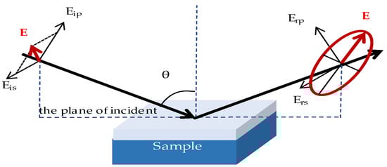
Figure 1.
Schematic diagram of the principle of spectroscopic ellipsometry.
The ellipsometric parameters, Psi (Ψ) and Delta (Δ), represent the changes in amplitude and phase of polarized light after reflection, respectively, and are defined as
where, ρ is the ellipsometry ratio; Ψ and Δ represent the amplitude ratio and phase difference, respectively; rp and rs are the Fresnel reflection coefficients in p-polarization and s-polarization; Erp and Eip represent the reflection and incident electric field strength of p-polarized light, respectively; Ers and Eis represent the reflected and incident electric field strength of s-polarized light, respectively. It can be seen from the above formula that the ellipsometry parameter depends on both the amplitude ratio and the phase difference between the p-polarized light and the s-polarized light, so the ellipsometry parameter is very sensitive to the surface topography.
The value of MSE is often used in ellipsometry analysis to describe the difference between the output ellipsometric parameters calculated by the optical model and the ellipsometric parameters obtained by the experimental measurement, indicating the quality of the fitting results. The formula for calculating MSE is:
where the subscript Model represents the spectral data of the model, the subscript SE represents the measured spectral data, n represents the number of wavelength points, m represents the total number of fitting parameters, and 2n represents the total number of points for the two parameters Ψ and Δ. After fitting, if the value of MSE is smaller, it indicates that the parameter fitting result is better, and the final fitting result is more credible; if the value of MSE is larger, it indicates that the parameter fitting result is poor, and the result is not credible, and other materials need to be combined. The characteristics and experimental characteristics parameters are verified to be reasonable. The experimental data are compared with the data generated by the model. According to the difference between the two sets of data, the model parameters are improved, and the optimal results are finally obtained.
2.2. Equivalent Medium Approximation Model
When ellipsometry is used to invert the optical constants of an object, the equivalent medium approximation (EMA) is often used to represent the ellipsometry response of the surface topography [,,,]. In the equivalent medium approximation model, the rough surface is equivalent to a new film, and its ellipsometric response is the same as the original surface. This film is a smooth film with only one medium, which is uniformly distributed in this layer, as shown in Figure 2. The equivalent thickness dEMA and the void volume fraction f are usually used to represent the geometric and optical properties of this new film.
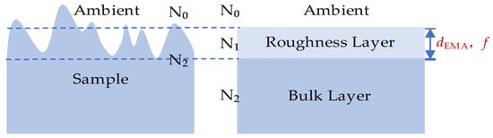
Figure 2.
Schematic diagram of the EMA model.
Within the EMA, roughness is replaced by a homogeneous fictitious layer with a certain thickness and dielectric function calculated using the Lorentz–Lorenz (LL), Maxwell Garnett (MG) or Bruggeman (BR) models. These models have the same generic formula, i.e., []
where, ε represents the dielectric constant of the equivalent mixed homogeneous medium, εh represents the dielectric constant of the material that occupies the main part in the original medium, εj and fj are the dielectric constant and the ratio of the jth component material in the medium, respectively, and γ is a coefficient related to the structural position of the constituent material.
In the LL EMA model, it is assumed that the environment can only be air or vacuum. In the MG EMA model, it is assumed that one medium wraps another medium. Obviously, these two calculation models do not correspond to the actual rough surface []. In comparison, the parameter void volume fraction is defined as the proportion of each medium contained in the roughness layer in Bruggeman EMA. Thus, the Bruggeman model in the EMA model has been widely used in the data processing of ellipsometric parameters to represent the roughness layer. The calculation formula is as follows []:
Among them, f represents the volume fraction of the raw material in the equivalent dielectric model layer, εn represents the dielectric function of the raw material; εvoid represents the dielectric function of the environment; εeff represents the dielectric of the new medium in the entire rough layer after equivalence function.
In the ellipsometry modeling analysis, different equivalent medium model layers can be established by changing the two parameters dEMA and f, but for the same rough surface structure, in order to make the ellipsometry response of the established EMA model the same as the original rough surface, when the MSE in the fitting is the smallest, there will be a mutual coupling relationship between the two parameters dEMA and f. One parameter increases or decreases, and the other parameter decreases or increases. Therefore, we often establish the equivalent medium model layer by fixing one of the parameters and fitting the other parameter. The MSE is the smallest and the fitting result is the best.
3. Simulation Results
Through the modeling function of the random rough surface in the software FDTD Solutions, the topographic characteristic parameters such as the average height h, the root mean square height σ and the correlation length τ are adjusted to explore the evolution of the ellipsometric parameters, and the relationship with the construction parameters of the equivalent medium model. The interfacial properties between Si and its thermally grown oxides are the most studied material because it is of technical importance and chemically the easiest semiconducting oxide system to fabricate, and therefore the most likely to be fundamentally understood. In this paper, the silicon and its oxide SiO2 are selected as research materials for the simulation [].
The basic components of a simulation for ellipsometry data analysis by using FDTD Solutions are: (1) Bloch boundary conditions (BBC) used in the four boundaries normal to the sample surface, (2) perfect matching for the top and bottom boundaries layer (PML), (3) a plane wave source with an incident angle θ, (4) a data monitor for recording the far-field projected electromagnetic field to calculate the ellipsometric parameters Ψ and Δ, (5) controlling the progress and end of the simulation conditional time monitor, and (6) sample structure [,,].
The position and simulation size of each component are introduced in detail, as shown in Figure 3. In the near-field simulation, the spacing between components needs to be greater than at least one wavelength range. Since the ellipsometric parameters need to be simulated in a wide spectral range under 400–1000 nm, the z-axis distances between the upper PML boundary and the data monitor, the data monitor and the light source, the light source and the substrate Si surface are all set to 2 μm, and the simulated boundary ranges in the x and y directions are all set to 1 μm.
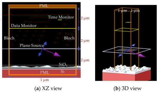
Figure 3.
The location diagram of each component in the (a) XZ view and (b) 3D view of the FDTD Solutions simulation interface.
The setting parameters of each component in the FDTD Solutions simulation are shown in Table 1, and other parameters are the default values of the software.

Table 1.
FDTD Solutions simulation setup parameter.
In order to verify the accuracy of the FDTD Solutions simulation ellipsometric parameters, the ellipsometric parameters were simulated for the structure of the smooth film, and the error range of the film thickness in the simulation was determined through forward modeling and parameter fitting, and the causes of the errors were analyzed.
Figure 4 shows the ellipsometric parameters of SiO2 films with a thickness of 2 nm, 50 nm, and 100 nm on silicon substrate under 65° incident angle in FDTD simulation. Figure 5 shows the thickness deviation fitted by the ellipsometric parameters of SiO2 film with thickness of 10~100 nm on silicon substrate under the 65° incident angle in FDTD simulation, and the angle fitting error is ignored at this time. It can be seen from the figure that the FDTD simulation ellipsometric parameters are more accurate for the structure with silicon substrate and SiO2 as the thin film. With a thickness of 100 nm, the error rate of FDTD is less than 1.2%, so the error meets the analysis conditions.
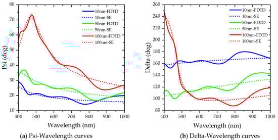
Figure 4.
Comparison of the ellipsometric parameters between FDTD simulation and forward modeling of smooth films of SiO2 films with thickness of 2 nm, 50 nm, and 100 nm on silicon substrate under 65° incident angle.
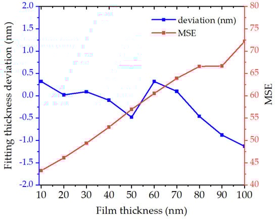
Figure 5.
Fitting Thickness deviation and MSE of FDTD simulated smooth thin films of SiO2 film with thickness of 10–100 nm on silicon substrate under the 65° incident angle.
From the above simulation ellipsometric parameters of the structure of the smooth film, it can be seen that the ellipsometry data results simulated by FDTD Solutions and the ellipsometry data obtained by forward modeling fit well, but there is still a certain degree of deviation. The reasons for the error are as follows: (1) The time setting is not long enough. After multiple reflections, the ellipsometry response produced by the structure is weak, but also affects the results of the ellipsometry data. The longer the simulation time is, the smaller data after multiple reflections of the film will be collected by the data monitor, making the results more accurate. (2) The simulation area is set smaller and the wavelength range of the light source is larger. The simulation area can be set larger, but the simulation time will be longer and the computer power requirement will be higher. (3) The step parameter is selected to be larger, and the mesh precision is set to be lower. Changes around a region were not captured in the simulation, which made the simulation results lack some reflection information about the film topography.
In naturally grown films, the surface topography is generally a random rough surface. The type is mostly Gaussian random micro-rough surface, which is the most widely used rough surface calculation method. It is generally determined by the average height h, the root mean square (rms) height σ and the correlation length τx and τy. The height function on a Gaussian random rough surface is as follows:
In the formula, and represent the undulation heights at the and position, respectively,
is the mean operator, h is the average height, σ is the root mean square height, τx and τy are the correlation lengths in the x and y directions, respectively, (x1, y1) and (x2, y2) are the coordinates of and , respectively.
When the 2D random rough surface does not consider the preferential roughness direction, it is equivalent to the isotropic rough surface. Figure 6 shows a Gaussian random rough surface with different rms heights and correlation lengths. When the height average h is 0, the roughness of the surface depends on the two parameters σ and τ. The smaller σ or the larger τ, the smoother the surface, and vice versa.
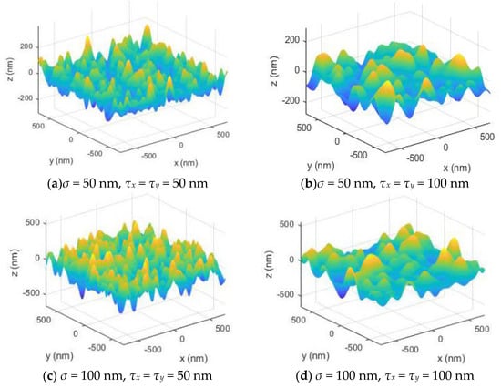
Figure 6.
Gaussian random rough surface with different σ and τ.
The default parameters are shown in Table 2. In the study of this section, when considering the change of one of the parameters, the other parameters are kept unchanged at their default values.
Table 2.
Default values of random rough surface parameters.
Different Gaussian random rough surfaces are generated in the FDTD Solutions software according to the above formula. Different structural models are established by changing the average height h, root mean square height σ, correlation length τx and τy, respectively, for the Gaussian random rough surface above the silicon substrate, the SiO2 film layer with a thickness of 100 nm and the rough layer.
The ellipsometry parameters for a 65° incidence angle in the wavelength range 400-1000 nm of the rough surface defined by the topographic feature parameters can be obtained by FDTD Solutions. Figure 7 shows the ellipsometric parameters of rough films under different surface topography characteristic parameters. Each topographic feature parameter was varied from 40 nm to 100 nm with 10 nm intervals. It can be seen that the topographic feature parameters such as the average height h, the root mean square height σ, and the correlation lengths τx and τy have a significant impact on Δ, and have little impact on Ψ. Under the same variation scale, the numerical offsets of the four topographic parameters to Ψ and Δ are also different. The topographic parameters corresponding to the offset order from large to small are: average height h, the root mean square height σ, and the correlation lengths τx and τy.
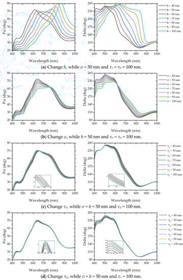
Figure 7.
Ellipsometric parameters with different surface topography parameters of the Gaussian random rough surface above the silicon substrate, the SiO2 film layer with a thickness of 100 nm and the rough layer.
As shown in Figure 8, the optical model established in ellipsometry analysis consists of Si substrate/SiO2 film/EMA layer/air, where the EMA layer is a mixture of SiO2 and air. The fixed parameters are that the incident angle θ is 65°, the thickness of the SiO2 film is 100 nm, and the fitting parameters are the thickness value dEMA in the EMA layer and the void volume fraction fSiO2 of the SiO2 material.
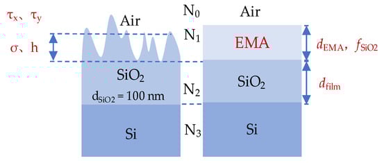
Figure 8.
Optical model established in ellipsometry analysis.
Figure 9 shows the fitting results of the ellipsometric parameters of the FDTD simulated rough films under different morphological parameters. It can be seen that the average height h, the root mean square height σ, the correlation lengths τx and τy all affect the values of the dEMA and fSiO2 parameters in the construction of the equivalent medium model, and they are all approximately linearly related, but the influencing coefficients are different.
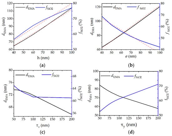
Figure 9.
Fitting results of ellipsometric parameters of rough surface simulated by FDTD under different topographic feature parameters.
Through the linear fitting of the data, the linear fitting relationship of each curve in Figure 9 can be obtained, as shown in Table 3. It can be seen from Table 3 that, as the characteristic parameters of longitudinal morphology, the average height h and root mean square height σ have more obvious influence on dEMA than that of fSiO2; as characteristic parameters of transverse morphology, correlation lengths τx and τy are more obvious for fSiO2 than dEMA, and the impact is more pronounced. As far as the influence coefficients are concerned, the correlation lengths τx and τy have too small and negligible effects on dEMA and fSiO2, and the average height h and the root mean square height σ are used as the characteristic parameters of longitudinal topography and cannot characterize the fSiO2 parameters.
Table 3.
The relationship between the topographic characteristic parameters (h, σ, τx and τy) of the random rough surface and the parameters of the EMA model.
Therefore, the influence of the average height h and the root mean square height σ on dEMA is mainly considered when establishing the equivalent medium model. According to the data in Table 3, dEMA = 35 + 0.80 h when σ = 50 nm, and dEMA = 25 + σ when h = 50 nm. When σ = 0 nm, the rough layer is a uniform film, and dEMA = 0, the equivalent thickness of the film is dr = h. Ignoring the influence of other factors, the parameter relationship for constructing the EMA model is dEMA = σ + 0.80 h.
In summary, when establishing the equivalent medium model, the selection of the parameter dEMA should mainly consider the average height h and the root mean square height σ in the longitudinal topographic characteristic parameters, that is, dEMA = σ + 0.80 h. The parameter fSiO2 should be chosen when the MSE is minimized.
4. Experimental Results
According to the simulation in the previous chapter, the relationship between the EMA parameters and the surface topography characteristic parameters can be obtained. In order to verify whether the laws we obtained through the simulation are in line with the actual situation, we have performed some experiments. By measuring the ellipsometric parameters and surface topography characteristic parameters of the film, different EMA model building methods are used to analyze the ellipsometry spectral data.
The surface micro-topography measuring instrument used in this paper is the ZYGO NewView 7300 Three-Dimensional Optical Surface Profiler. The ellipsometry data measuring instrument used in the experiments is the Wide-Spectrum Mueller matrix ME-L Ellipsometer, which is developed by Wuhan Eoptics Technology Co., Ltd. (Wuhan, China). The sample is measured in reflectance measurement mode. The detection spot is an ellipse, the diameter of the short axis of the ellipse is about 3 mm, and the diameter of the long axis is related to the incident angle. Before measuring the ellipsometer, we need to perform precise calibration of the instrument, including the oblique incidence calibration and angle calibration of the optical path. The angular calibration is defined as the ellipsometric parameters of a pure silicon wafer at an incident angle of 65°. Therefore, the ellipsometric parameters of the sample at the incident angle of 65° are mainly measured, and the accuracy is relatively high, in the experimental measurement.
The morphological characteristic parameters were fitted and analyzed under the conditions of no EMA layer and an established EMA layer. We have established three models for analysis: without EMA layer, with EMA layer (f = 50%, dEMA unknown), and with EMA layer (dEMA = σ + 0.80 h, f unknown). The above three models are established in turn. Ellipsometry and surface measurements were performed on pure substrates ((a) sapphire and (b) silicon carbide) and thin films ((c) SiO2 and (d) perovskite films) with rough surfaces, respectively.
Figure 10 shows the ellipsometry measurement and fitting results. It indicates that the fitting effect when establishing EMA is better than that when not establishing EMA, and the ellipsometry parameters established by using the model of dEMA = σ + 0.80 h are more in line with the measured parameters.
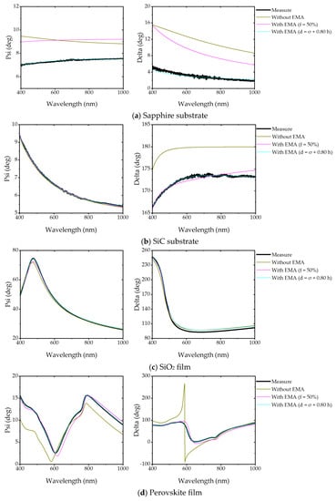
Figure 10.
Fitting curves of measured ellipsometric parameters and without EMA layer and with established EMA layer. (a,b) represent bare sapphire and bare silicon carbide substrate, respectively; (c) represents silicon substrate with silicon oxide thin film; (d) represents perovskite thin film deposited on the sapphire substrate.
For these four different materials, model 1, model 2, and model 3 were established, respectively, for fitting. The fitting data of ellipsometry and the measured topographic feature parameter data are shown in Table 4, which mainly compares the data results and MSE of the four materials when the three models are fitted. Table 4 indicates that the MSE obtained by fitting becomes smaller and smaller for evaluating the modelling performance from model 1 to model 3, and the uncertainties of the equivalent thickness dEMA of the rough layer for four materials and the film thickness dfilm for SiO2 and perovskite films are also becoming smaller and smaller. Since the surface roughness of the SiO2 film is too small, there is little difference when using these three models, respectively, but the data error range with the Model 3 is smaller than that of the other two models. This means that the established EMA model conforms to the surface structure of the actual sample and has better precision.
Table 4.
Experimental results of the samples from four materials with three models.
In summary, the EMA model with the relationship of dEMA = σ + 0.80 h was created by measuring the ellipsometric parameters and surface topography parameters by a wide-spectrum ellipsometer and a 3D optical profiler, and it can be applied to sapphire, silicon carbide, silicon dioxide and perovskite materials with micro-rough surfaces.
5. Conclusions
In this paper, the equivalent approximation medium model of rough, thin films is studied by the method of combining simulation and experiment. The finite time domain difference (FDTD) method can be used to simulate the ellipsometric parameters of different structures according to the definition of ellipsometry. The ellipsometric parameters of rough films with different morphological parameters were simulated by FDTD Solutions, and it was found that the selection of the parameter dEMA should mainly consider the average height h and the root mean square height σ in the longitudinal morphological parameters, that is, dEMA = σ + 0.80 h. The void volume fraction f should be selected as the fitting result when MSE is the smallest. Using dEMA = σ + 0.80 h to build the EMA model can relate the ellipsometry data to the topographic data of the rough surface, instead of just using f = 50% to represent the surface roughness. By measuring the ellipsometric parameters and surface topography characteristic parameters of different rough films, if an equivalent approximation medium model is constructed, the ellipsometry spectrum curve can be better fitted and more accurate optical properties can be obtained. The results from this work may facilitate a better understanding and utilization for the EMA model in SE.
Author Contributions
Conceptualization, W.Y. and C.C.; methodology, W.Y., H.L. and S.B.; software, W.Y. and S.B.; validation, W.Y., C.C. and H.L.; formal analysis, W.Y. and H.L.; investigation, W.Y.; resources, W.Y., C.C. and X.C.; data curation, W.Y. and X.C.; writing—original draft preparation, W.Y. and X.C.; writing—review and editing, W.Y., C.C. and S.B.; visualization, W.Y.; supervision, W.Y.; project administration, W.Y. and C.C.; funding acquisition, C.C. All authors have read and agreed to the published version of the manuscript.
Funding
This research was funded by the Fujian Science and Technology (Grant No. 2020I0101).
Institutional Review Board Statement
Not applicable.
Informed Consent Statement
Informed consent was obtained from all subjects involved in the study.
Data Availability Statement
The data that support the findings of this study are available from the corresponding author upon reasonable request.
Acknowledgments
The authors would like to thank Zhanhua Wei of College of Materials Science and Engineering, Huaqiao University, Jiayuan Wang of Xiamen University, Jun Qiu of Harbin Institute of Technology, Hao Jiang of Huazhong University of Science and Technology, and Ke Wang of East China University of Technology.
Conflicts of Interest
The authors declare no conflict of interest.
References
- Castriota, M.; Politano, G.G.; Vena, C. Variable Angle Spectroscopic Ellipsometry investigation of CVD-grown monolayer graphene. Appl. Surf. Sci. 2019, 467–468, 213–220. [Google Scholar] [CrossRef]
- Ohlídal, I.; Lukeš, F.E. Analysis of semiconductor surfaces with very thin native oxide layers by combined immersion and multiple angle of incidence ellipsometry. Appl. Surf. Sci. 1988, 35, 259–273. [Google Scholar] [CrossRef]
- Zheng, Z.; Luo, Y.; Yang, H. Thermal tuning of terahertz metamaterial properties based on phase change material vanadium dioxide. Phys. Chem. Chem. Phys. 2022, 24, 8846–8853. [Google Scholar] [CrossRef]
- Chen, H.; Chen, Z.; Yang, H. Multi-mode surface plasmon resonance absorber based on dart-type single-layer graphene. RSC Adv. 2022, 12, 7821–7829. [Google Scholar] [CrossRef] [PubMed]
- Zhao, F.; Lin, J.; Lei, Z. Realization of 18.97% theoretical efficiency of 0.9 µm Thick c-Si/ZnO Heterojunction Ultrathin-film Solar Cells via Surface Plasmon Resonance Enhancement. Phys. Chem. Chem. Phys. 2022, 24, 4871–4880. [Google Scholar] [CrossRef] [PubMed]
- Zheng, Z.; Zheng, Y.; Luo, Y. A switchable terahertz device combining ultra-wideband absorption and ultra-wideband complete reflection. Phys. Chem. Chem. Phys. 2022, 24, 2527–2533. [Google Scholar] [CrossRef] [PubMed]
- Wu, X.; Zheng, Y.; Luo, Y. A four-band and polarization-independent BDS-based tunable absorber with high refractive index sensitivity. Phys. Chem. Chem. Phys. 2021, 23, 26864–26873. [Google Scholar] [CrossRef]
- Derkowska-Zielinska, B.; Skowronski, L.; Biitseva, A. Optical characterization of heterocyclic azo dyes containing polymers thin films. Appl. Surf. Sci. 2017, 421, 361–366. [Google Scholar] [CrossRef]
- Johnson, P.B.; Christy, R.W. Optical constants of copper and nickel as a function of temperature. Phys. Rev. B 1975, 11, 1315–1323. [Google Scholar] [CrossRef]
- Zhang, Y.; Zhou, X.; Cao, K. Ellipsometry study on Pd thin film grown by atomic layer deposition with Maxwell–Garnett effective medium approximation model. Thin Solid Film. 2015, 593, 144–149. [Google Scholar] [CrossRef]
- Muneshwar, T.; Cadien, K. Probing initial-stages of ALD growth with dynamic in situ spectroscopic ellipsometry. Appl. Surf. Sci. 2015, 328, 344–348. [Google Scholar] [CrossRef]
- Luria, O.; Mohapatra, P.K.; Patsha, A. Large-Scale characterization of Two-Dimensional Monolayer MoS2 Island Domains Using Spectroscopic Ellipsometry and Reflectometry. Appl. Surf. Sci. 2020, 524, 146418. [Google Scholar] [CrossRef]
- Saini, M.; Augustine, S.; Ranjan, M. In-plane optical anisotropy and SERS detection efficiency of self-organized gold nanoparticles on silicon nanoripples: Roles of growth angle and postgrowth annealing. Appl. Surf. Sci. 2020, 512, 145703. [Google Scholar] [CrossRef]
- Li, D.; Song, X.; Xu, J. Optical properties of thickness-controlled MoS2 thin films studied by spectroscopic ellipsometry. Appl. Surf. Sci. 2017, 421, 884–890. [Google Scholar] [CrossRef]
- Li, H.; Cui, C.; Xu, X. A review of characterization of perovskite film in solar cells by spectroscopic ellipsometry. Sol. Energy 2020, 212, 48–61. [Google Scholar] [CrossRef]
- Fujiwara, H. Spectroscopic Ellipsometry Principles and Applications; John Wiley & Sons: Hoboken, NJ, USA, 2007. [Google Scholar]
- Fang, S.J.; Chen, W.; Yamanaka, T. Comparison of Si surface roughness measured by atomic force microscopy and ellipsometry. Appl. Phys. Lett. 1996, 68, 2837–2839. [Google Scholar] [CrossRef]
- Li, D.; Zhang, W.; Goullet, A. Influence of PECVD-TiO2 film morphology and topography on the spectroscopic ellipsometry data fitting process. Mod. Phys. Lett. B 2020, 34, 2050228. [Google Scholar] [CrossRef]
- Chen, R.; West, J.C. Analysis of scattering from rough surfaces at large incidence angles using a periodic-surface moment method. IEEE Trans. Geosci. Remote Sens. 1995, 33, 1206–1213. [Google Scholar] [CrossRef]
- Ohlídal, I.; Vohánka, J.; Čermák, M. Optical characterization of randomly microrough surfaces covered with very thin overlayers using effective medium approximation and Rayleigh–Rice theory. Appl. Surf. Sci. 2017, 419, 942–956. [Google Scholar] [CrossRef]
- Koh, J.; Lu, Y.; Wronski, C.R. Correlation of real time spectroellipsometry and atomic force microscopy measurements of surface roughness on amorphous semiconductor thin films. Appl. Phys. Lett. 1996, 69, 1297–1299. [Google Scholar] [CrossRef]
- Petrik, P.; Biró, L.P.; Fried, M. Comparative study of surface roughness measured on polysilicon using spectroscopic ellipsometry and atomic force microscopy. Thin Solid Films 1998, 315, 186–191. [Google Scholar] [CrossRef]
- Fujiwara, H.; Kondo, M.; Matsuda, A. Real-time spectroscopic ellipsometry studies of the nucleation and grain growth processes in microcrystalline silicon thin films. Phys. Rev. B 2001, 63, 115306. [Google Scholar] [CrossRef]
- Yanguas-Gil, A.; Sperling, B.A.; Abelson, J.R. Theory of light scattering from self-affine surfaces: Relationship between surface morphology and effective medium roughness. Phys. Rev. B 2011, 84, 085402. [Google Scholar] [CrossRef]
- Qiu, J.; Ran, D.F.; Liu, Y.B. Investigation of ellipsometric parameters of 2D microrough surfaces by FDTD. Appl. Opt. 2016, 55, 5423–5431. [Google Scholar] [CrossRef]
- Chen, Y.; Wang, J.; Xu, T. FDTD simulation of the optical properties for a gold nanoparticle-over-nanosheet hybrid structure. Curr. Appl. Phys. 2020, 20, 391–399. [Google Scholar] [CrossRef]
- Gkogkou, D.; Shaykhutdinov, T.; Oates, T.W.H. Characterization of anisotropically shaped silver nanoparticle arrays via spectroscopic ellipsometry supported by numerical optical modeling. Appl. Surf. Sci. 2017, 421, 460–464. [Google Scholar] [CrossRef]
- Taflove, A.; Hagness, S.C.; Piket-May, M. The Electrical Engineering Handbook—Computational Electromagnetics; Elsevier Inc.: Amsterdam, The Netherlands, 2005. [Google Scholar]
- Narayan, S.; Divya, K.; Kanth, V. FDTD Modeling of EM Field inside Microwave Cavities; Springer: Cham, Switzerland, 2017. [Google Scholar]
- Santos, A.J.; Lacroix, B.; Maudet, F. Surface oxidation of amorphous Si and Ge slanted columnar and mesoporous thin films: Evidence, scrutiny and limitations for infrared optics. Appl. Surf. Sci. 2019, 493, 807–817. [Google Scholar] [CrossRef]
- Zhou, F.; Qin, F.; Yi, Z. Ultra-wideband and wide-angle perfect solar energy absorber based on Ti nanorings surface plasmon resonance. Phys. Chem. Chem. Phys. 2021, 23, 17041–17048. [Google Scholar] [CrossRef]
- Tompkins, H.G.; Irene, E.A. Handbook of Ellipsometry; William Andrew: Norwich, NY, USA, 2005. [Google Scholar]
- Hilfiker, J.; Tompkins, H. Spectroscopic Ellipsometry—Practical Application to Thin Film Characterization; Momentum Press: New York, NY, USA, 2016. [Google Scholar]
- Bruggeman, D.A.G. Berechnung verschiedener physikalischer Konstanten von heterogenen Substanzen. III. Die elastischen Konstanten der quasiisotropen Mischkörper aus isotropen Substanzen. Ann. Phys. 1937, 421, 160–178. [Google Scholar] [CrossRef]
- Aspnes, D.E.; Theeten, J.B.; Hottier, F. Investigation of effective-medium models of microscopic surface roughness by spectroscopic ellipsometry. Phys. Rev. B 1979, 20, 3292–3302. [Google Scholar] [CrossRef]
- Qiu, J.; Ting Wu, Y.; Huang, Z. A Hybrid Partial Coherence and Geometry Optics Model of Radiative Property on Coated Rough Surfaces. J. Heat Transf. 2013, 135, 091010. [Google Scholar] [CrossRef]
- Losurdo, M.; Hingerl, K. Ellipsometry at the Nanoscale; Springer: Cham, Switzerland, 2013. [Google Scholar]
- Aspnes, D.E.; Theeten, J.B. Spectroscopic Analysis of the Interface Between Si and Its Thermally Grown Oxide. J. Electrochem. Soc. 2019, 127, 1359–1365. [Google Scholar] [CrossRef]
- Cheung, K.T.; Foo, Y.; To, C.H. Towards FDTD modeling of spectroscopic ellipsometry data at large angles of incidence. Appl. Surf. Sci. 2013, 281, 2–7. [Google Scholar] [CrossRef]
- Foo, Y.; Cheung, K.T.; To, C.H. On the development of Finite-Difference Time-Domain for modeling the spectroscopic ellipsometry response of 1D periodic structures. Thin Solid Films 2014, 571, 356–363. [Google Scholar] [CrossRef]
- Foo, Y.; Zapien, J.A. Convergence and precision characteristics of finite difference time domain method for the analysis of spectroscopic ellipsometry data at oblique incidence. Appl. Surf. Sci. 2017, 421, 878–883. [Google Scholar] [CrossRef]
Publisher’s Note: MDPI stays neutral with regard to jurisdictional claims in published maps and institutional affiliations. |
© 2022 by the authors. Licensee MDPI, Basel, Switzerland. This article is an open access article distributed under the terms and conditions of the Creative Commons Attribution (CC BY) license (https://creativecommons.org/licenses/by/4.0/).