Review

Bridgman Method for Growing Metal Halide Single Crystals: A Review

1
College of Engineering, Shandong Xiehe University, Jinan 250109, China
2
School of Materials Science and Engineering, Shandong University, Jinan 250061, China
*
Authors to whom correspondence should be addressed.
These authors contributed equally to this work.
Inorganics 2025, 13(2), 53; https://doi.org/10.3390/inorganics13020053
Submission received: 9 January 2025 / Revised: 7 February 2025 / Accepted: 10 February 2025 / Published: 11 February 2025
(This article belongs to the Special Issue Advanced Inorganic Semiconductor Materials, 2nd Edition)

Abstract

:
The Bridgman method for single-crystal growth enables the formation of crystals at the lower end of the molten material by cooling it under a precisely controlled temperature gradient. This makes it particularly suitable for producing high-quality single-crystal materials. Over the years, the Bridgman technique has become widely adopted for growing single crystals of semiconductors, oxides, sulfides, fluorides, as well as various optoelectronic, magnetic, and piezoelectric materials. Recently, there has been growing interest in metal halide materials, with the growth of high-quality metal halide single crystals emerging as a major focus for both the scientific community and industry. However, traditional solution-based single-crystal growth methods have several limitations, such as slow growth rates, inconsistent crystal quality, challenges in solvent selection, and difficulties in controlling saturation levels. These issues present significant obstacles, particularly when large, defect-free, high-quality single crystals are needed for certain high-performance materials. As a result, the Bridgman method has emerged as an effective solution to overcome these challenges. This review provides an overview of various categories of metal halide single-crystal systems grown using the Bridgman method in recent years. The systems are classified based on their dimensionality into three-dimensional, two-dimensional, and zero-dimensional metal halide structures. Furthermore, we highlight novel metal halide single crystals developed through the Bridgman technique. Additionally, we offer a brief introduction to the structures, properties, and applications of these single crystals, underscoring the crucial role of the Bridgman method in advancing research in this field.

1. Introduction

The Bridgman method for single-crystal growth is a pivotal technique, which has been extensively utilized in the preparation of single crystals for semiconductor materials, optoelectronic devices, and other high-performance materials [1,2,3]. First proposed by the American scientist Theodore Bridgman in 1915, it has since evolved into one of the most established technologies for producing single crystals with high quality [4]. The Bridgman method is renowned for its process stability, precise controllability, and stringent material requirements, making it a fundamental technique in materials science, particularly in research focused on high-purity and high-quality single crystals [5,6,7].

1.1. Basic Principle

As illustrated in Figure 1a, the Bridgman method operates on the principle of the dissolution-crystallization process [8,9,10,11]. Through controlling the temperature gradient precisely, the material within the solution gradually cools, facilitating the transition from the liquid solution to solid state, thereby yielding a single crystal. In this process, the material is first heated above its melting point to form a liquid phase, and then it is progressively cooled under a controlled temperature gradient, promoting the crystallization of the material from liquid state to solid status [12,13]. The Bridgman method is particularly effective for materials with high melting points that can maintain stability at elevated temperatures, such as certain semiconductor materials, ceramics, and metal alloys [14].
It should be noted that there are necessary ways to determine the appropriate method in advance for growing different halide single crystals. In other words, not all halide single crystals can be grown using the Bridgman method. Although a large body of previous work suggests that potential halides can be predicted using simulation methods, growing these potential halide single crystals faces significant uncertainty [15,16]. A phase diagram is a concise graphical representation of the relationship between the components, temperature, and pressure of a system at thermodynamic equilibrium. Initially, phase diagrams were obtained through extensive experiments [17]. With the development of computational materials science, computational phase diagrams based on molecular dynamics have become an efficient method for obtaining phase diagrams [18,19,20]. For halides, by referencing phase diagrams of related components, it is possible to determine whether the single crystal of the compound is likely to grow easily [21]. Taking the binary phase diagram of chlorides as an example, a large number of previous works have summarized the synthesis conditions of approximately one thousand halides, including their melting points, whether they fully crystallize, lattice structures, and space groups [22]. In the relevant literature, researchers have even been able to compile statistics on how many reported works have successfully grown halide single crystals and the preparation methods they used. In the future, as more and more new halides are successfully synthesized, these phase diagrams will continue to expand, becoming a reference handbook for researchers. It should be noted that, compared to solution-based crystal growth, the progress of phase diagrams in this field will be slower because methods for growing large single crystals, such as the Bridgman method, require more expensive and larger-scale growth equipment, which is not always available for researchers.

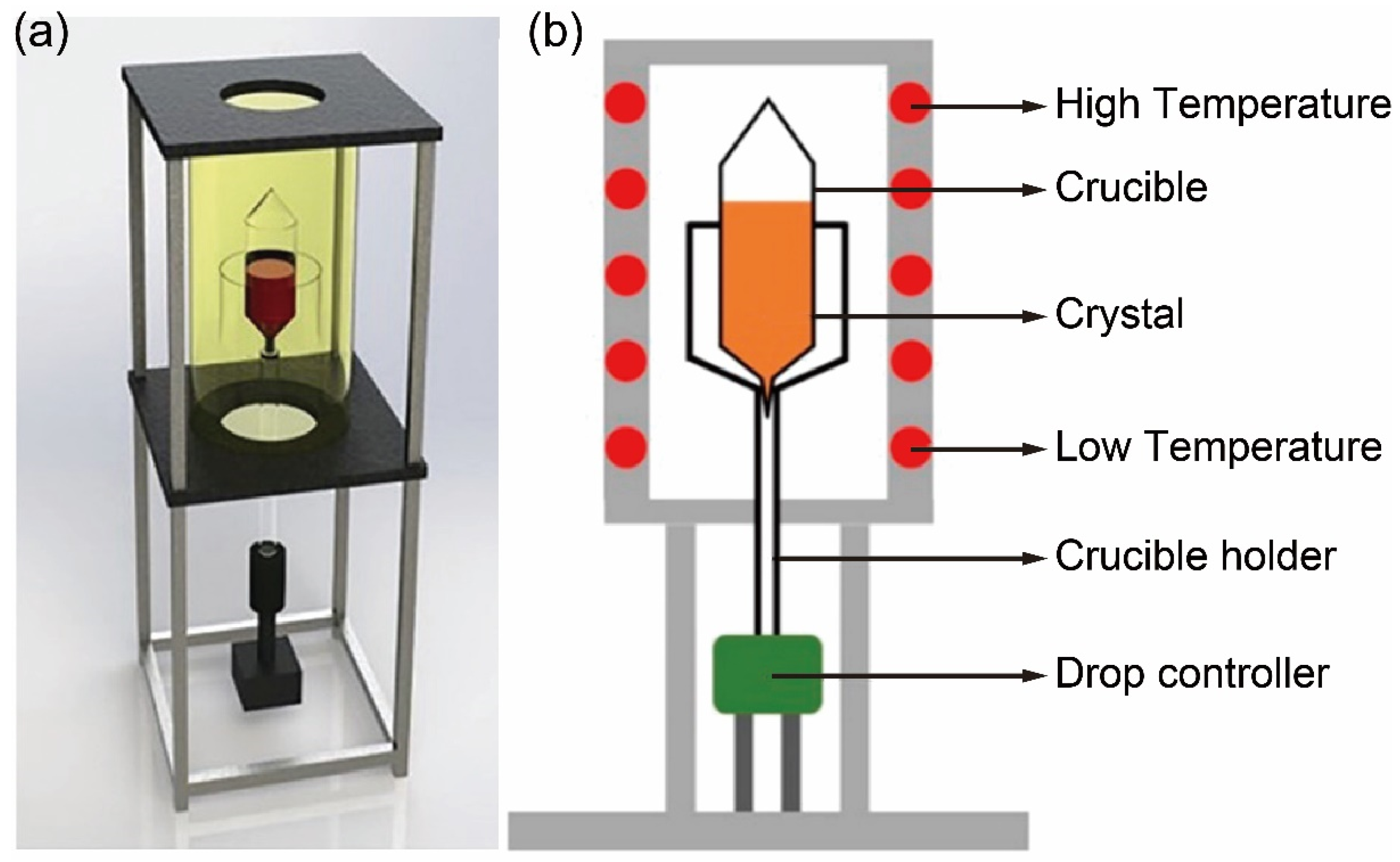
1.2. Experimental Setup for the Bridgman Method

As exhibited in Figure 1b, the experimental setup for the Bridgman method comprises several essential components: a high-temperature furnace, a crucible, a cooling system, and a temperature gradient control system [8,23]. The high-temperature furnace is used to heat the crucible and create a high-temperature environment for the process. The furnace’s temperature control system allows for precise regulation of the heating temperature and distribution, ensuring uniform heating and melting of the material [24]. The crucible serves as the container for the material to be crystallized and is typically constructed from high-temperature-resistant materials such as quartz or platinum [25]. The selection of the crucible material must account for both chemical stability and resistance to high temperatures. The Bridgman method relies on a cooling process to guide the material from liquid phase to a solid state [26]. Therefore, a cooling system is essential to facilitate this phase of the process. Water or air cooling systems are commonly employed to regulate the cooling rate. During this process, precise control over the temperature gradient is critical. The temperature gradient is a key factor influencing the success of the Bridgman method [27]. By controlling the temperature range of the furnace and the cooling system, a suitable temperature gradient can be maintained from the top to the bottom of the crucible, thereby promoting the preparation of high-quality single crystals.
Figure 1. (a) Three-dimensional diagram of a typical Bridgman furnace. Reprinted with permission from Ref. [8]. Copyright 2021, Royal Society of Chemistry. (b) Planar graph of vertical Bridgman furnace and their key assemblies. Reprinted with permission from Ref. [23]. Copyright 2018, American Chemical Society.
Inorganics 13 00053 g001

1.3. Growth Process

The growth process using the Bridgman method for single crystals is typically divided into several stages. First, the raw materials intended for crystal growth are placed in the crucible and heated above their melting point to ensure complete transition into the liquid phase. During the melting process, it is crucial to maintain a stable temperature to prevent excessive bubble formation or the introduction of undesirable impurities [28]. Once the material has fully melted, the next step involves establishing a reasonable temperature gradient by adjusting the high/low-temperature zone. This gradient is achieved by gradually moving the crucible from the high-temperature zone to the lower-temperature zone [29]. Generally, the temperature at the bottom zone is lower, while the top remains hotter. This temperature differential prompts the material to begin crystallizing at the bottom of the crucible, initiating the growth of single crystals. As the temperature decreases, the material transitions from a liquid state to a solid phase. Under the influence of the temperature gradient, crystal nuclei begin to form in the lower-temperature region of the crucible. As the solution becomes supersaturated, crystals start to deposit on the liquid’s surface. The process must proceed slowly to ensure smooth crystal growth and the formation of a single, high-quality crystal [30]. Over time, the crystal grows steadily out of the liquid and increases in size. When the crystal reaches the desired size, mechanical methods are employed to extract it from the crucible. To minimize the risk of damaging the crystal during removal, the temperature is typically lowered gradually to room temperature, and protective measures are implemented [31]. After extraction, further processing, such as cutting and polishing, is often conducted to achieve the certain shape and surface quality of the crystal [32].

1.4. Advantages of the Bridgman Method

The Bridgman method, as a traditional technique for single-crystal growth, offers several distinct advantages. First and foremost, it provides precise control over the temperature gradient, a critical factor in achieving high-quality single crystals [33]. The accuracy of temperature regulation directly impacts the quality of as-prepared crystals, making this feature particularly significant. Additionally, the Bridgman method is versatile, suitable for single-crystal growth from wide ranges of materials, including metals, semiconductors, ceramics, and more [34,35]. It is especially advantageous for growing materials with high melting points. Moreover, as the Bridgman method involves a transition from liquid state to solid phase, impurities in the liquid solution are effectively excluded, resulting in single crystals with high purity [36].
The Czochralski method, as another popular technology for single crystal growth, has often been compared to Bridgman method [37]. The Czochralski method is widely used in semiconductor materials and the single crystal growth of high-tech industries such as silicon and germanium [38]. Its advantages include higher growth rate, that the Czochralski method stretches the crystal while it is in a molten state, which results in a relatively fast growth rate, making it suitable for large-scale production [39]. Moreover, since the crystal is gradually stretched in a molten state, more uniform crystals with higher purity can be obtained. In addition, this method is capable of growing large single crystals, suitable for industrial production [40]. However, the Czochralski method has several disadvantages. For example, the equipment for this method is more complex and requires precise control of temperature, stretching rate, and other parameters, thus making it more expensive. In addition, since the crystal is grown by stretching, the process may introduce more defects, especially when not operating under suitable conditions [41].
In summary, the Bridgman method is suitable for high-melting-point materials and precision-demanding applications, but it has a slower growth rate, limited crystal size, and lower cost. The Czochralski method is better suited for large-scale production and single crystals with high purity and uniformity, but the equipment is more complex, costly, and has a limited range of applicability.

1.5. Current Mainstream Applications

The Bridgman method is extensively utilized for synthesis of single crystals for semiconductor materials, ceramics, and corresponding optoelectronic devices [34,35,42]. In the semiconductor industry, for instance, the Bridgman method is employed to grow high-quality single crystals such as gallium arsenide (GaAs), indium phosphide (InP), and other compounds [43,44]. The aforementioned materials are widely applied in fields such as integrated circuits, laser diodes, and solar cells. Additionally, the Bridgman method plays a crucial role in the research and development of high-temperature superconducting materials, ferroelectric materials, and other advanced materials [45,46,47,48,49].
Metal halide materials have garnered considerable attention due to their outstanding photoelectronic properties, particularly their promising potentials in photovoltaics, photocatalysis, and light-emitting devices [15,16,50,51]. For example, all-inorganic perovskite nanocrystal CsPbBr3 has been used as scintillators to provide convenient visualization tool for X-ray radiography [52]. In addition, recent studies indicate that CsPbBr3 nanocrystals can also be applied in quantum computing and quantum communications owing to their excellent single-photon feature when assembled to be superlattice [51]. Metal halides with lower dimensions possess unique properties. For example, zero-dimensional Cs2MoCl6 and Cs2WCl6 single crystals emit near-infrared light, which can be used in safety inspection and night vision [53]. Low-dimensional organic–inorganic hybrid metal halides as subgroup halide compounds have been widely used in optoelectronic domains. For example, one-dimensional (C5H11N3)MnCl2Br2·H2O exhibited water-molecule-induced reversible photoluminescence transformation, which has been used in anti-counterfeiting field [54].
Metal halide materials are characterized by high melting points and a strong sensitivity to impurities, which means that the single-crystal growth process demands precise control over factors including temperature, liquid concentration, and cooling speed [55,56,57,58]. The Bridgman method operates by gradually cooling the material under a controlled temperature gradient, facilitating the transition from liquid state to solid phase. This method allows for effective regulation of both the crystal growth rate and its quality. Moreover, the crystal quality and growth rate of metal halide single crystals are closely dependent on the temperature gradient [59]. The Bridgman method excels in providing a uniform and stable temperature gradient throughout the growth process, making its temperature control capabilities essential for producing high-quality single crystals. Additionally, the cooling process inherent in the Bridgman method effectively excludes impurities, ensuring the formation of high-purity crystals. The removal of impurities is crucial for enhancing the optoelectronic performance of metal halide materials [60]. Furthermore, given the high melting points of many metal halide materials, the Bridgman method’s capacity to operate at elevated temperatures makes it particularly well-suited for growing perovskite materials, which require high-temperature conditions [61].

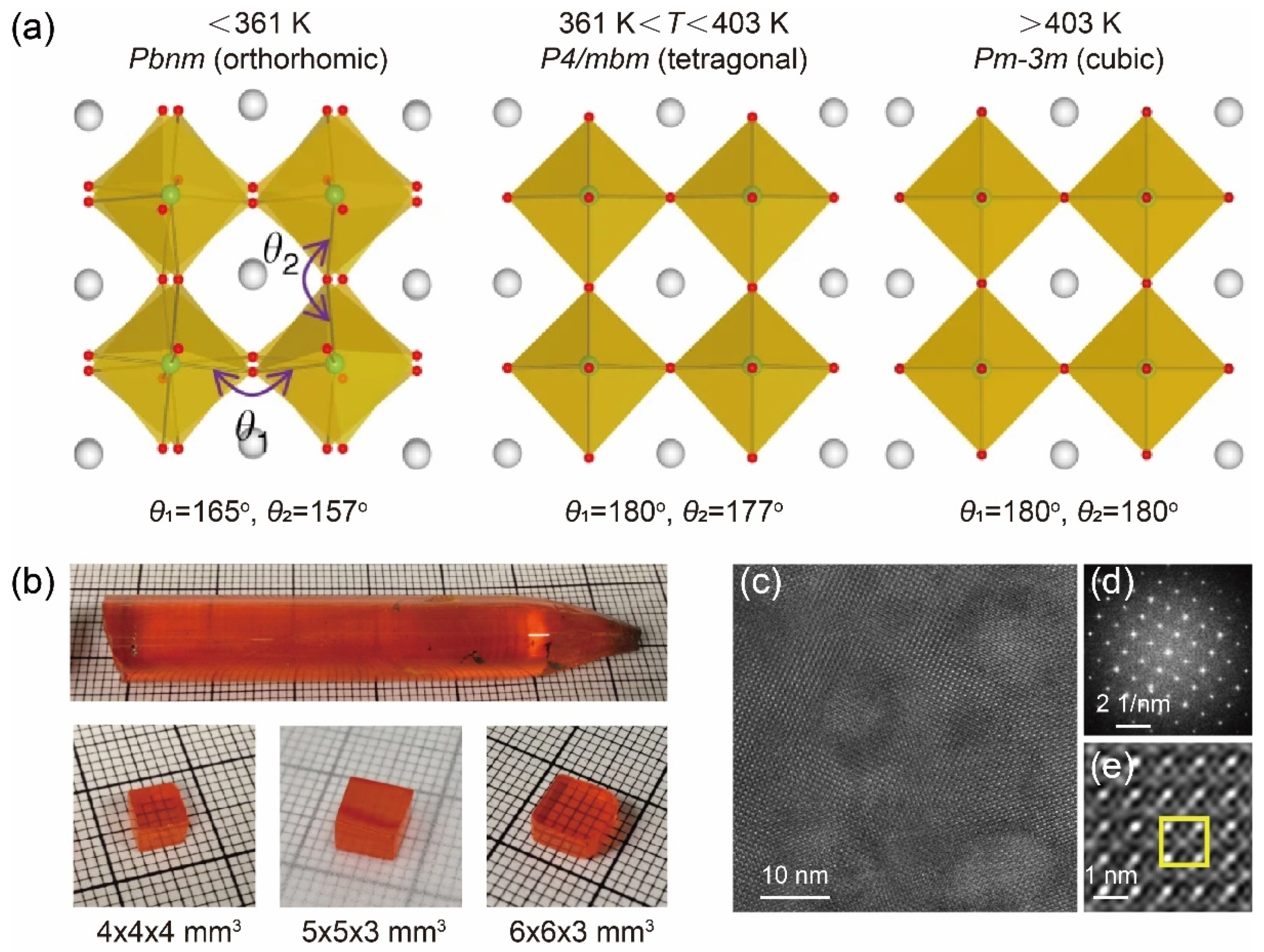
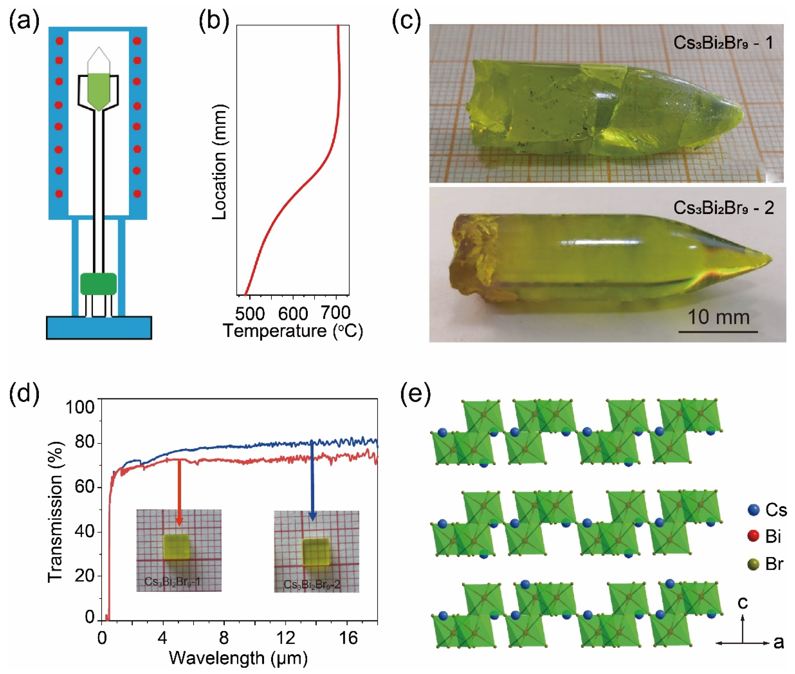
2. Bridgman Method for Growing Three-Dimensional Metal Halide Single Crystals

Three-dimensional (3D) metal halides represent the largest subgroup of metal halides, distinguished by their unique crystal structures and exceptional optoelectronic properties [62,63,64,65,66]. In recent years, they have attracted widespread attention in fields such as optoelectronic devices, photovoltaics, photocatalysis, and light-emitting diodes (LEDs) [67,68]. Three-dimensional metal halides are known for their excellent light absorption properties, including broad absorption spectra and efficient absorption cross-sections, which make them highly effective in energy conversion applications, particularly in photovoltaic devices [69,70]. Notably, in solar cells, 3D metal halides can achieve high energy conversion efficiencies even under low light intensities, positioning them as a key area of research in solar energy. In addition to their optical properties, 3D metal halides exhibit large carrier mobility and excellent carrier diffusion, which makes them highly efficient for use in electronic devices [71,72,73].
However, 3D metal halides are easily to be degraded when exposed to water and oxygen, which can significantly impair their optoelectronic performance [74,75]. As a result, enhancing the environmental stability and longevity of these materials has become a major focus of ongoing research. Fortunately, large-sized 3D metal halide single crystals prepared by the Bridgman method have demonstrated significantly improved stability [76,77,78]. Research in this area has experienced rapid growth in recent years, offering promising prospects for addressing these challenges.
Three-dimensional metal halides often undergo nondestructive phase transitions at relatively low temperatures [79]. Taking CsPbBr3 as an example, as shown in Figure 2a, the first phase transition occurs around 403 K, where the material shifts from the cubic phase to tetragonal configuration, with the feature of first-order phase transition. After that, a second-order transition occurs at 361 K to the orthorhombic phase, which finally becomes stable at room temperature [80]. However, residual stress still exists after these transitions, which can induce mechanical deformation and crack formation. Such imperfections can significantly degrade the properties of detectors, highlighting the importance of carefully managing these transitions during the crystal growth process.
In a recent study, researchers presented an enhanced Bridgman method for growing CsPbBr3 single crystals, significantly improving their optoelectronic performance [80]. The as-grown CsPbBr3 single crystals, with dimensions reaching several centimeters, exhibit exceptionally low impurity concentrations (below 10 ppm across a total of 69 elements). The critical process in this work is the modification of growth parameters, which leads to large-sized, crack-free single crystals, as shown in Figure 2b. It is important to highlight that the precise control of kinetic parameters during the crystal growth process is critical. Parameters including temperature gradient and cooling rate play pivotal roles, and have been meticulously optimized through growing many times. Notably, the impurity concentration in final products is below 10 ppm, with impurities exceeding 0.5 ppm likely being introduced from the precursor materials. Additionally, the optical transmittance is higher than 65% for wavelengths greater than 600 nm and exceeds 80% for wavelengths above 1000 nm. These findings confirm that the CsPbBr3 single crystals exhibit exceptional chemical purity, which is one of the distinct advantages of the Bridgman method [81]. The single-crystallinity and outstanding uniformity of the CsPbBr3 crystals were verified through selected area electron diffraction (SAED) and high-resolution transmission electron microscopy (HRTEM) with fast Fourier transform (FFT) analysis, as shown in Figure 2c–e. No precipitates were detected in these single crystals, further confirming their high chemical purity. Consequently, the scalable growth of 3D CsPbBr3 single crystals underscores the potential of metal halides as exceptional next-generation materials for photoelectric applications [82,83].
In another study, large-sized 3D CsPbBr3 single crystals were grown using an optimized Bridgman method, as shown in Figure 3a [23]. After determining the crystallographic directions using the X-ray orientation technique, the anisotropic optoelectronic properties of the material were investigated for the first time. To examine the optoelectronic anisotropy, photoresponse measurements were performed on the (100), (010), and (001) crystallographic planes, as shown in Figure 3b. The three CsPbBr3 single crystal devices possessed distinct anisotropic optoelectronic properties. The responsivity and external quantum efficiency (EQE) of the best plane demonstrated a three-fold improvement compared to other planes. This unique behavior can be attributed to the structural anisotropy of CsPbBr3, which determines the charge carrier’s transport. The anisotropic electron-transport properties in CsPbBr3 single crystals were further characterized, as shown in Figure 3c [84]. In the current–voltage curves, Ohmic, trap-filling, and Child regions were detected as the bias voltage increased. These results reveal a pronounced anisotropy in the electron transport properties, with superior electron transport observed along a certain direction. This is due to the variations in the carrier transport within the crystal structure [85,86,87]. Consequently, the exceptional optoelectronic properties of CsPbBr3 single crystals prepared via the Bridgman method are expected to inspire further exploration of their potential for high-performance optoelectronic applications.
The detection of γ-rays with high energy resolution remains the most challenging applications today [88,89,90]. Even the smallest presence of defects can significantly degrade the signal generated by γ-rays, making semiconductor detectors relatively rare. However, lead halide perovskite semiconductors exhibit exceptional defect tolerance, resulting in outstanding and unique optoelectronic properties [91,92,93]. As a result, these materials are poised to have a transformative impact on applications in photoelectric conversion and radiation detection. In a recent study, researchers demonstrated that CsPbCl3 single crystals grown by the Bridgman method can act as high-performance detectors for γ-ray radiation [94]. Similarly to CsPbBr3, CsPbCl3 undergoes two phase transitions: from the cubic to the tetragonal phase at 325 K, followed by a transition to the orthorhombic phase at 316 K, which finally becomes stable at room temperature (Figure 4a) [95]. Large-scale CsPbCl3 single crystals were synthesized using the Bridgman method, as shown in Figure 4b. The resulting CsPbCl3 crystal exhibits pale-yellow with high optical transparency. The optical transmission exceeds 80% for wide light wavelengths, as shown in Figure 4c. This high transparency indicates that CsPbCl3 single crystals contain few impurities. The optical absorption edge was around 425 nm, corresponding to a wide bandgap of 2.90 eV. Therefore, the wide-bandgap CsPbCl3 single crystals obtained through the Bridgman method hold significant potential for γ-ray detection [96,97,98].
The Bridgman method can also be used to grow 3D metal halide single crystals with mixed compositions [99,100,101,102]. In a recent study, series of large-sized perovskite single crystals CsPbBr3−3nX3n were fabricated by the modified Bridgman method through precisely controlling the synthesis parameters, as exhibited in Figure 5a [8]. The sharp absorption edges in the absorption spectra indicate the direct-band-gap feature of these perovskite single crystals, as depicted in Figure 5b. Furthermore, the absorption edges of them are continuously tunable, corresponding to wide bandgaps, by only adjusting the halide composition [103]. Consequently, perovskite single crystals with mixed halogens exhibit considerable potential as filter-free photodetectors.

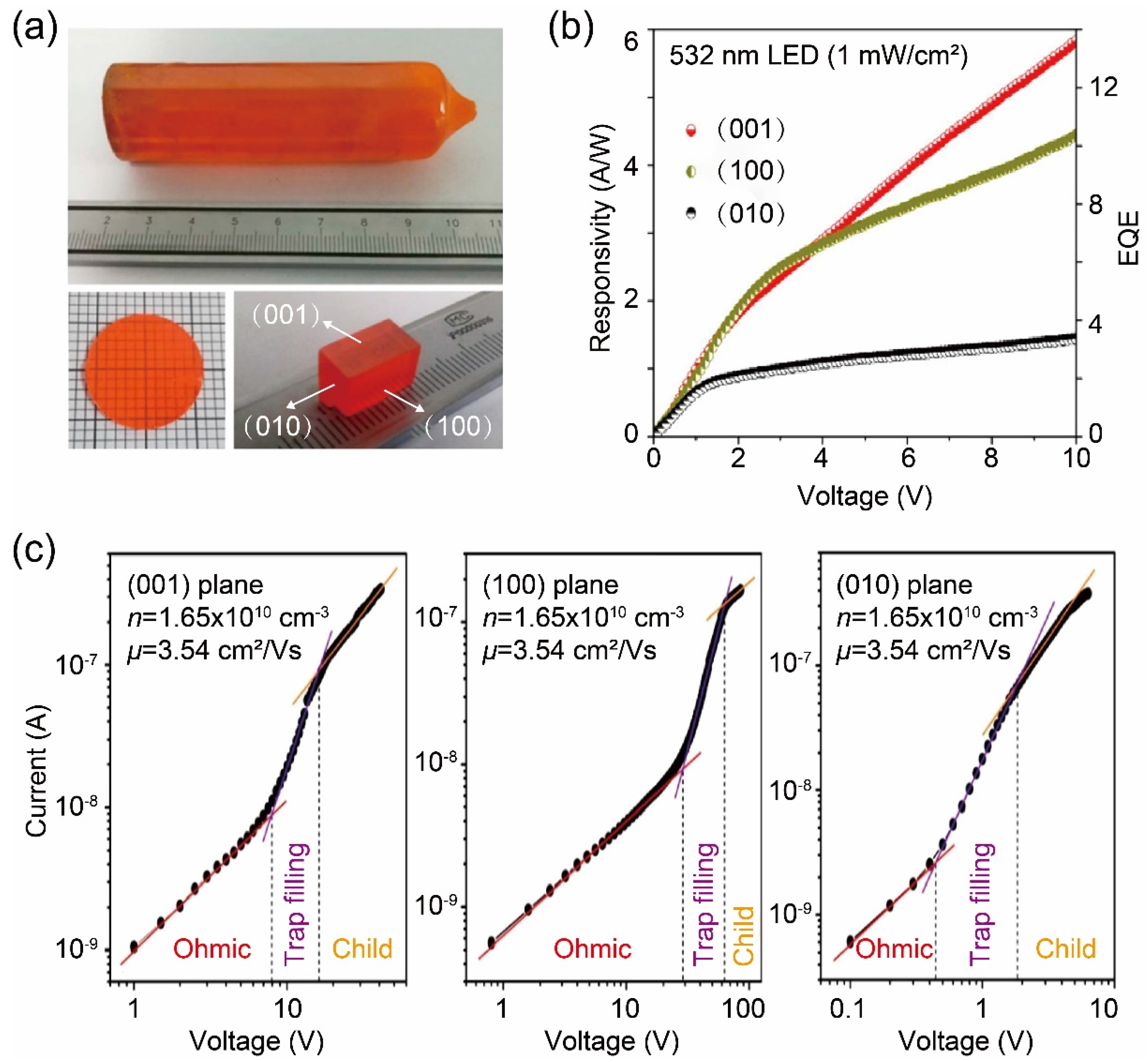
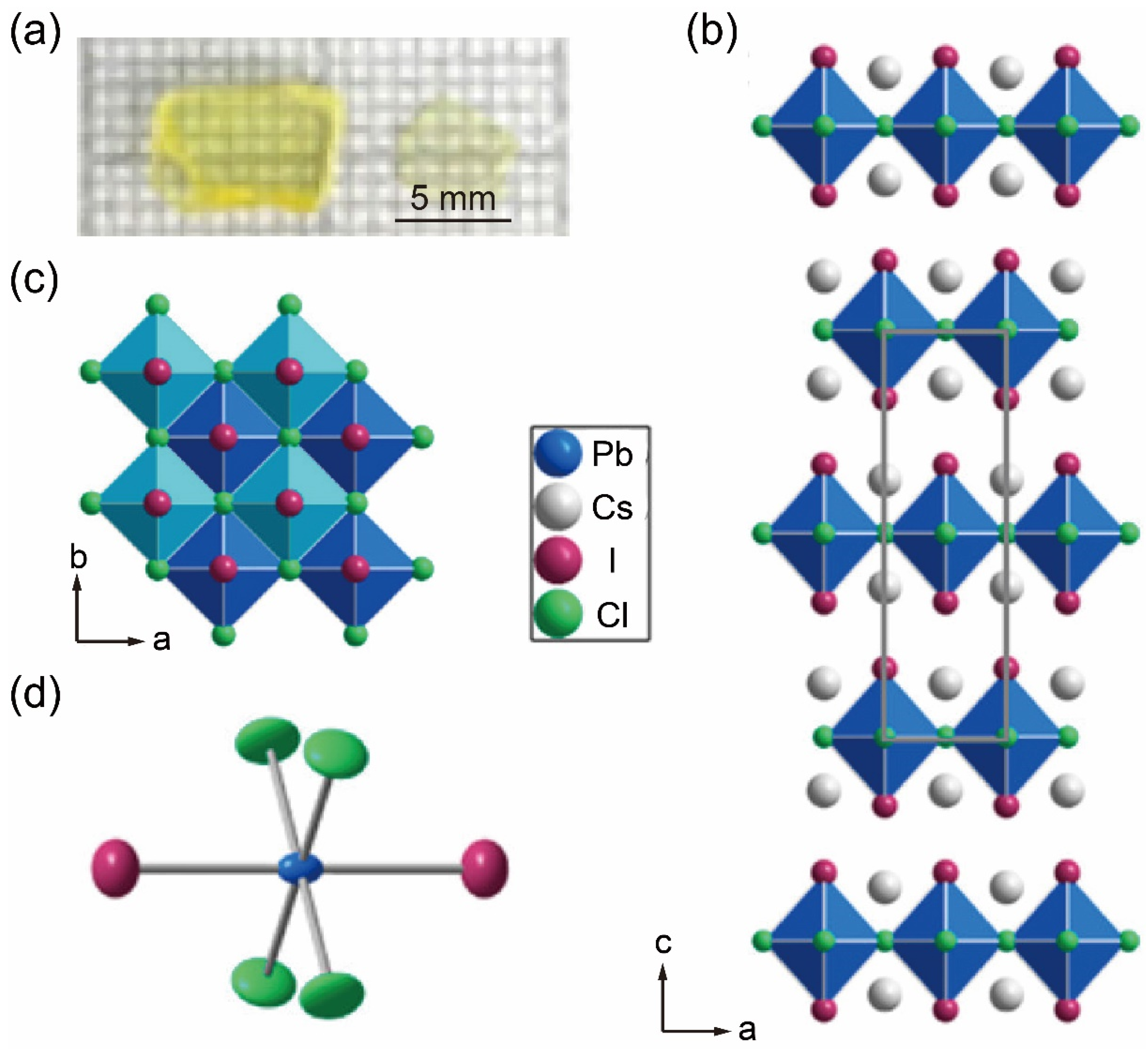
3. Bridgman Method for Growing Two-Dimensional Metal Halide Single Crystals

The two-dimensional (2D) Ruddlesden–Popper (RP) phases constitute a significant class of metal halides, characterized by their diverse and remarkable optoelectronic properties [104,105,106]. To date, the majority of hybrid RP phases incorporate long organic spacers [107,108]. However, conventional synthesis methods are predominantly limited to the growth of 2D RP metal halides with organic components. In another word, all-inorganic 2D RP metal halides cannot be prepared. In other words, synthesizing all-inorganic 2D RP metal halides presents significant challenges.
Recent studies have successfully synthesized all-inorganic 2D RP Cs2PbI2Cl2 single crystals using the Bridgman method, as shown in Figure 6a [79,109]. These crystals are nearly centimeter-sized, significantly larger than those obtained through solution-based methods. Cs2PbI2Cl2 adopts the K2NiF4-type configuration and crystallizes in tetragonal phase, as illustrated in Figure 6b–d [110]. The 2D [PbI2Cl2]2− plane is composed of corner-sharing Pb-centered [PbI2Cl4]4− units. In addition, Cl ions occupy in-plane sites, behaving as shared corners of octahedra, while I ions occupy out-of-plane sites as terminal ligands. Cs⁺ spacer ions balance the charge, resulting in a standard single-layer (n = 1) RP structure. Density functional theory calculations, along with experimental findings, support the thermodynamic stability of these single crystals. Further computational analysis indicates that Cs2PbI2Cl2 behaves as a direct bandgap semiconductor with low effective carrier mass towards in-plane direction, which aligns with the experimentally obtained in-plane photoresponse [111,112]. The successful growth of Cs2PbI2Cl2 by the Bridgman method not only expands the family of 2D metal halides but also opens new possibilities for applications beyond photovoltaics.
Subsequent efforts were made by researchers to grow larger single crystals using the Bridgman method. Through meticulous adjustment of synthesis parameters, including the cooling rate, temperature gradient, and post-heat treatment, large-sized single crystals were successfully achieved, as exhibited in Figure 7a [113]. Structural analysis reveals that the single-layer RP structure is composed of corner-sharing [PbI2Cl4]4− octahedral units, as depicted in Figure 7b. Further investigations confirm that the remarkable phonon transport properties of Cs2PbI2Cl2, driven by lone-pair-driven octahedral rotations and anharmonic lattice dynamics, which demonstrates the potential for novel thermal transport behavior across a broad range of low-dimensional metal halide perovskites [114].

4. Bridgman Method for Growing Zero-Dimensional Metal Halide Single Crystals

In recent years, less toxic metals such as Sn, Sb, and Bi have attracted considerable attention as environmentally friendly alternatives to Pb [115,116,117,118,119]. Among these, low-dimensional Bi-based halide materials have emerged as promising candidates for optoelectronic applications [120,121,122]. Notably, all-inorganic zero-dimensional (0D) bismuth-halide single crystals of Cs3Bi2X9 (X = Br and I) have been successfully synthesized using the Bridgman method.
As shown in Figure 8a, a custom-designed semitransparent Bridgman furnace has been developed to enable real-time monitoring and precise adjustment of crystal growth parameters during the synthesis process [123]. This innovative furnace facilitated the optimization of the thermal profile for growing high-quality Cs3Bi2Br9 single crystals, as illustrated in Figure 8b. Using this modified Bridgman method, large-sized single crystals Cs3Bi2Br9 were successfully synthesized. To minimize structural defects and prevent crystal cracking, small temperature gradient and slow growth rates have been proved essentially. Specifically, slower rates were employed to grow transparent, crack-free Cs3Bi2Br9-2 crystals, while faster rates resulted in cracked Cs3Bi2Br9-1 crystals, as shown in Figure 8c. Figure 8d displays the optical transmittance spectra of these two single crystals. Both exhibit a broad transparency range with no significant absorption features. Notably, Cs3Bi2Br9-2 demonstrates an average transmittance of approximately 80% in the range of 2 µm to over 18 µm, surpassing the ~70% transmittance of Cs3Bi2Br9-1. At room temperature, Cs3Bi2Br9 crystallizes into trigonal system, with its crystal structure depicted in Figure 8e [124]. The layered perovskite structure of Cs3Bi2Br9 can be regarded as a tripling of typical perovskite unit cell, where only partial octahedra are fully occupied. The remaining octahedra form corrugated, vacant layers that separate the occupied layers. This arrangement enables a corner-sharing configuration of [BiBr6] octahedra [125].
Subsequently, researchers proposed a mixed-halogen strategy to fine-tune the structural dimensions and optoelectronic properties of Cs3Bi2I9-nBrn [126]. High-quality single crystals, with dimensions reaching up to ten centimeters, were successfully grown using the Bridgman technique, as depicted in Figure 9a. By incorporating iodine into the 0D Cs3Bi2Br9 framework, the optoelectronic properties were systematically modified. Among these, Cs3Bi2I8Br emerged as the most promising candidate, demonstrating negligible ion migration, moderate resistivity, and superior carrier transport capabilities. The halogen-mixing strategy offers a pathway to balance carrier transport properties with resistivity in targeted compositions, optimizing performance for applications such as X-ray detection. Notably, Cs3Bi2I8Br was identified as the optimal composition, achieving a record-breaking sensitivity of 1.74 × 10⁴ μC Gy−1 cm−2. This sensitivity is second only to the 6.3 × 10⁴ μC Gy−1 cm−2 achieved by Pb-based CsPbBr2.9I0.1 single crystals under 120 keV hard X-ray detection. Furthermore, X-ray detectors fabricated from Cs3Bi2I8Br single crystals demonstrated exceptional long-term stability in ambient air, ultralow dark current drift, and robust high-resolution imaging performance even at elevated temperatures. This combination of properties underscores the material’s potential for next-generation X-ray detection technologies [127,128].
The optical and electronic properties of Bridgman-grown single crystals of wide-bandgap semiconducting halide perovskites A3M2I9 (A = Cs, Rb; M = Bi, Sb) have been extensively studied [130]. Intense Raman scattering was observed at room temperature for all compounds, indicating high polarizability and pronounced electron–phonon coupling [129]. Strong evidence of electron–phonon interactions, comparable to those found in alkali halides, was revealed through phonon broadening in the photoluminescence emission spectra, as shown in Figure 9c,d. Effective phonon energies, derived from temperature-dependent photoluminescence measurements, aligned well with the observed Raman peak energies. Based on these findings, a model has been proposed wherein electron–phonon interactions in Cs3Sb2I9, Rb3Sb2I9, and Cs3Bi2I9 generate small polarons, resulting in exciton trapping by the lattice. The recombination of these self-trapped excitons accounts for the broad photoluminescence emission. Additionally, Rb3Bi2I9, Rb3Sb2I9, and Cs3Bi2I9 exhibit high resistivity and strong photoconductive responses under laser photoexcitation. These characteristics suggest that these compounds are promising candidates for semiconductor applications, particularly in the detection of hard radiation.

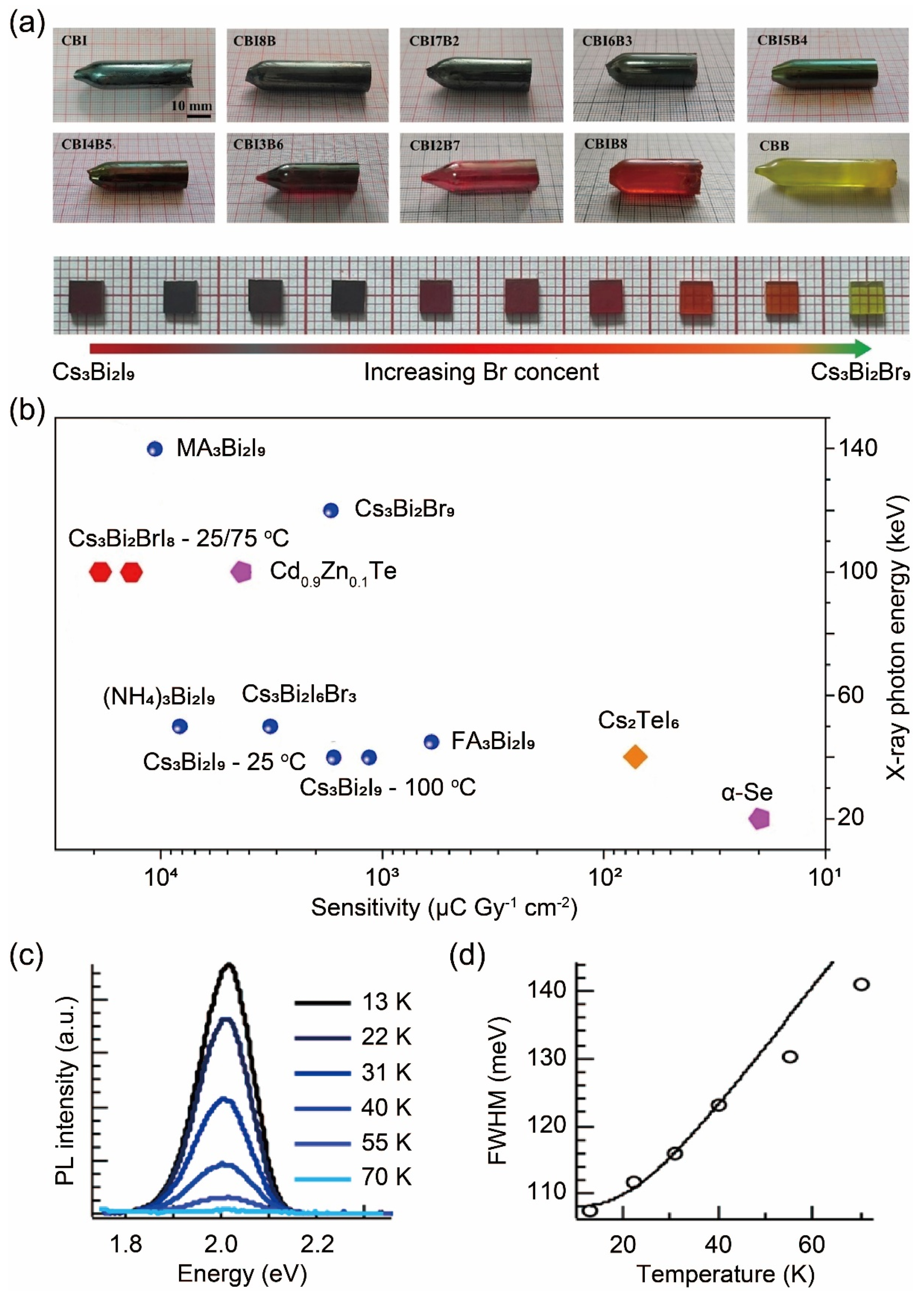
5. Bridgman Method for Growing Novel Metal Halide Single Crystals

5.1. Cs3Cu2I5 Single Crystals

Low-dimensional Cu(I) metal halides, known for their efficient exciton emissions, have recently gained attention as promising scintillation materials for X-ray and gamma-ray detection [131,132,133]. A recent study demonstrated the potential of 0D Cs3Cu2I5 as a sensitive thermal neutron detector with effective neutron–gamma discrimination achieved through lithium doping [134,135]. Single crystals of Cs3Cu2I5 doped with 95% enriched 6Li were successfully grown using the Bridgman method, as illustrated in Figure 10a. As shown in Figure 10b, Cs3Cu2I5:6Li exhibits impressive performance metrics, including an energy resolution of 4.8% for 662 keV 137Cs gamma rays, a high light yield of 30,000 photons/MeV for gamma rays, and 96,000 photons/neutron for thermal neutrons. Additionally, it achieves a robust neutron–gamma pulse shape discrimination figure of merit of 2.27 using Power Spectral Density (PSD) waveforms. This breakthrough discovery of 0D metal halide single crystals, specifically Cs3Cu2I5:6Li, represents a significant advancement in the development of stable, high-performance scintillators for neutron–gamma detection applications [136,137].
In another study, Tl cations were successfully incorporated into the Cs3Cu2I5 host using the Bridgman method, leading to the development of an ultrabright and highly efficient scintillator for X-ray and γ-ray detection, as shown in Figure 10c [138]. The Tl-doped Cs3Cu2I5 single crystals achieved an impressive photoluminescence quantum efficiency of 79.2%. Under X-ray excitation, the radioluminescence emission of Cs3Cu2I5:Tl crystals featured a self-trapped exciton emission at 440 nm and a Tl-related emission at 510 nm at room temperature. Optimized Tl doping resulted in a nearly fivefold enhancement of the steady-state scintillation yield, reaching up to 150,000 photons/MeV, alongside a significant improvement in X-ray detection sensitivity, which decreased from 103.6 to 66.3 nGy s−1. Additionally, the material exhibited an exceptionally low afterglow of just 0.17% at 10 ms after X-ray cutoff. The Cs3Cu2I5:Tl scintillator demonstrated outstanding performance, including an energy resolution of 3.4% at 662 keV and an ultrahigh light yield of 87,000 photons/MeV under 137Cs γ-ray radiation, rivaling the capabilities of commercial scintillators, as illustrated in Figure 10d [140,141].
Based on the aforementioned studies, it can be concluded that doping-modified Cs3Cu2I5 single crystals exhibit significant potential as X-ray detection materials, primarily due to their efficient exciton emissions arising from strongly localized charge carriers [142,143,144,145,146,147]. However, many of these materials still display scintillation yields well below their theoretical maxima [148]. A recent study demonstrated that the charge carrier harvesting efficiency could be significantly enhanced by introducing a small amount of indium (In) doping into these highly localized structures [139]. Bright 0D Cs3Cu2I5:In single crystals were synthesized via the Bridgman method, exhibiting efficient and tunable dual emissions. All samples were transparent and free of inclusions, as shown in Figure 10e. Under X-ray excitation, the radioluminescence emission of Cs3Cu2I5:In crystals featured a self-trapped exciton emission at 460 nm and an In⁺-related emission at 620 nm at room temperature. In doping significantly enhanced the photoluminescence quantum efficiency of Cs3Cu2I5from 68.1% to 88.4%. To assess the impact of In doping on X-ray imaging performance, undoped and 0.2% In-doped Cs3Cu2I5 single crystals were utilized as scintillation screens in an X-ray imaging system. As depicted in Figure 10f, the In-doped Cs3Cu2I5 crystals achieved an exceptional spatial resolution of 18 lp mm−1, surpassing commercial CsI:Tl-based flat-panel X-ray detectors, all-inorganic perovskite nanocrystal scintillators, and thermally activated delayed fluorescence (TADF) organic scintillator-based X-ray imaging detectors (≈6 lp mm−1) [52,149]. This remarkable spatial resolution is attributed to the superior transparency, reduced light scattering, and enhanced scintillation yield of Cs3Cu2I5 single crystals compared to commercial polycrystalline thick films or fluorescent powders. These advancements position Cs3Cu2I5:In as a highly promising candidate for next-generation X-ray imaging applications.

5.2. Tl-Containing Single Crystals

Materials containing thallium (Tl) often exhibit strong fluorescence, making Tl-doped crystals highly suitable as scintillators for high-energy radiation detection [150,151,152,153]. In fact, such scintillators are widely utilized today. For instance, Tl-doped sodium antimonite (NaSb:Tl) crystals are known for their high scintillation efficiency and excellent radiation response, making them a common choice for particle detectors [150]. Additionally, Tl-doped magnesium aluminate (MgAl2O4:Tl) is recognized for its exceptional thermal stability and high light output, while Tl-doped cesium chloride (CsCl:Tl) is frequently employed for neutron detection, as Tl significantly enhances the material’s sensitivity to neutrons [154,155,156,157]. Similarly, Tl-doped cesium fluoride (CsF:Tl) scintillators exhibit a high light yield, making them ideal for radiation detection and particle physics experiments. As a result, Tl-containing scintillators are extensively applied across diverse fields, including nuclear physics, radiation monitoring, medical imaging, and particle detection, underscoring their importance in advancing high-energy detection technologies [158].
In a recent study, centimeter-sized TlPbI3 single crystals were successfully grown using the Bridgman method, as illustrated in Figure 11a [159]. TlPbI3 exhibits a unique crystal structure within the halides, distinguishing itself from conventional perovskites by belonging to the broader class of perovskite-like compounds. It crystallizes in the orthorhombic space group Cmcm and adopts the CaIrO3 structure type, as shown in Figure 11b [160]. The structure consists of alternating layers of [PbI3] units interspersed with Tl⁺ ions. Within the 2D layers, the axially compressed [PbI6/2] octahedra expand anisotropically in the perovskite plane. These octahedra are connected via edge-sharing (PbI4/2 connectivity) along the shorter a-axis and corner-sharing (PbI2/2 connectivity) along the longer c-axis. The Tl atoms adopt a trigonal prismatic coordination geometry [161]. The bandgap structure of TlPbI3 is mainly determined by Pb 6s and Tl 6s states deriving from the lone pair electrons in Pb2+ and Tl+ [159]. As we all know, metal elements often result in quite different electronic structures and properties in halide compounds [162,163]. The 5s electron pair of Pb2+ results in high tolerance against defects, therefore better stability of TlPbI3 is often obtained than their counterparts such as CsPbI3 [164]. Another study indicates that stronger bonding between Tl and I is the main cause of better stability of TlPbI3 than CsPbI3, owing to the lower total energy [165]. Furthermore, due to their different configurations of perovskite structure in CsPbI3 and perovskite-like structure in TlPbI3, they possess significantly disparate properties. For example, stronger bonding interactions in TlPbI3 lead to more dispersive band edges, which increases the bandwidth and reduces the bandgap [166]. Moreover, the enhanced dispersion of band edges makes less effective carrier masses and anisotropic transport features.
TlPbI3 demonstrates high electrical resistivity of approximately 1012 Ω·cm. Detectors fabricated from these single crystals show robust photoresponsiveness to Ag Kα X-rays (22.4 keV) and are capable of detecting 122 keV γ-rays from a 57Co radiation source. The electron mobility-lifetime product was measured at 1.8 × 10⁻⁵ cm2·V−1. Furthermore, TlPbI3 exhibits a high relative static dielectric constant of 35.0, indicating its strong capability to screen carrier scattering and suppress the effects of charged defects. These characteristics position TlPbI3 as a promising material for high-energy radiation detection applications [164,166,167].
Figure 11. (a) Image of a pristine TlPbI3 single crystal. (b) The crystal structure of TlPbI3 with the left panel providing an overview of the structure. The right panels focus on the connectivity along the [PbI3] layers and the coordination environment around the Tl⁺ ions, respectively. Reprinted with permission from Ref. [159]. Copyright 2021, Wiley-VCH GmBH. (c) Image of the TlSn2I5 single crystal. (d) The antiperovskite structure of TlSn2I5. Reprinted with permission from Ref. [168]. Copyright 2017, American Chemical Society.
Inorganics 13 00053 g011
In addition to TlPbI3, the semiconductor TlSn2I5, which features a two-dimensional crystal structure and an antiperovskite topology, has emerged as a promising novel material for radiation detection applications [169]. TlSn2I5 incorporates elements with high atomic numbers (Tl: 81, Sn: 50, I: 53) and a relatively high density (6.05 g·cm−3), ensuring a superior absorption coefficient compared to both halide perovskites and CdZnTe in response to hard radiation. In a recent study, centimeter-sized TlSn2I5 single crystals were successfully grown using the Bridgman method, as shown in Figure 11c [168]. As illustrated in Figure 11d, when viewed without considering chemical bonding constraints, the lattice formed by I, Tl, and Sn adopts an antiperovskite structure. In this arrangement, iodine is positioned at the center of an axially elongated octahedron, with its equatorial plane occupied by four Sn ions and its polar positions filled by two Tl ions. This results in the formation of a cationic [ISn2Tl]4+ framework. This framework exhibits a distorted perovskite structure, with the octahedra tilting out-of-phase in a manner similar to that observed in the hybrid perovskite CH3NH3PbI3, which crystallizes in the non-centrosymmetric I4/mcm space group due to the asymmetric CH3NH3 +cation. However, compared to CH3NH3PbI3, TlSn2I5 demonstrates superior long-term stability, enhanced photon stopping power, higher resistivity (~1010 Ω·cm), and robust mechanical properties. Additionally, TlSn2I5 can be utilized to fabricate detector devices capable of detecting Ag Kα X-rays (22 keV), 57Co γ-rays (122 keV), and 241Am α-particles (5.5 MeV). The mobility-lifetime product and electron mobility were estimated to be 1.1 × 10⁻³ cm2·V−1 and 94 ± 16 cm2·V−1·s−1, respectively. Notably, unlike other halide perovskites, TlSn2I5 exhibits no evidence of ionic polarization under prolonged high-voltage bias, further highlighting its suitability for long-term, stable operation in radiation detection applications.

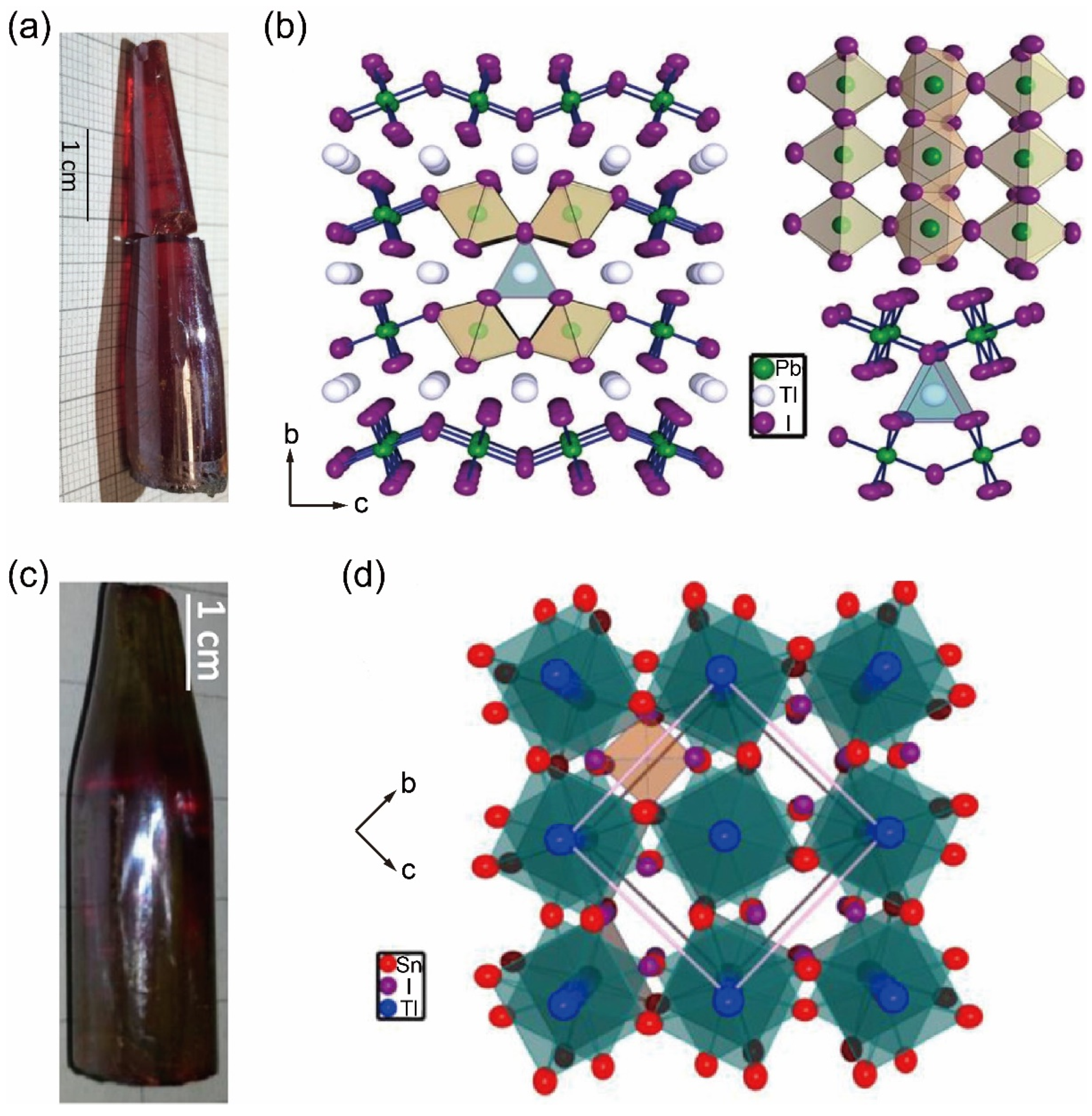
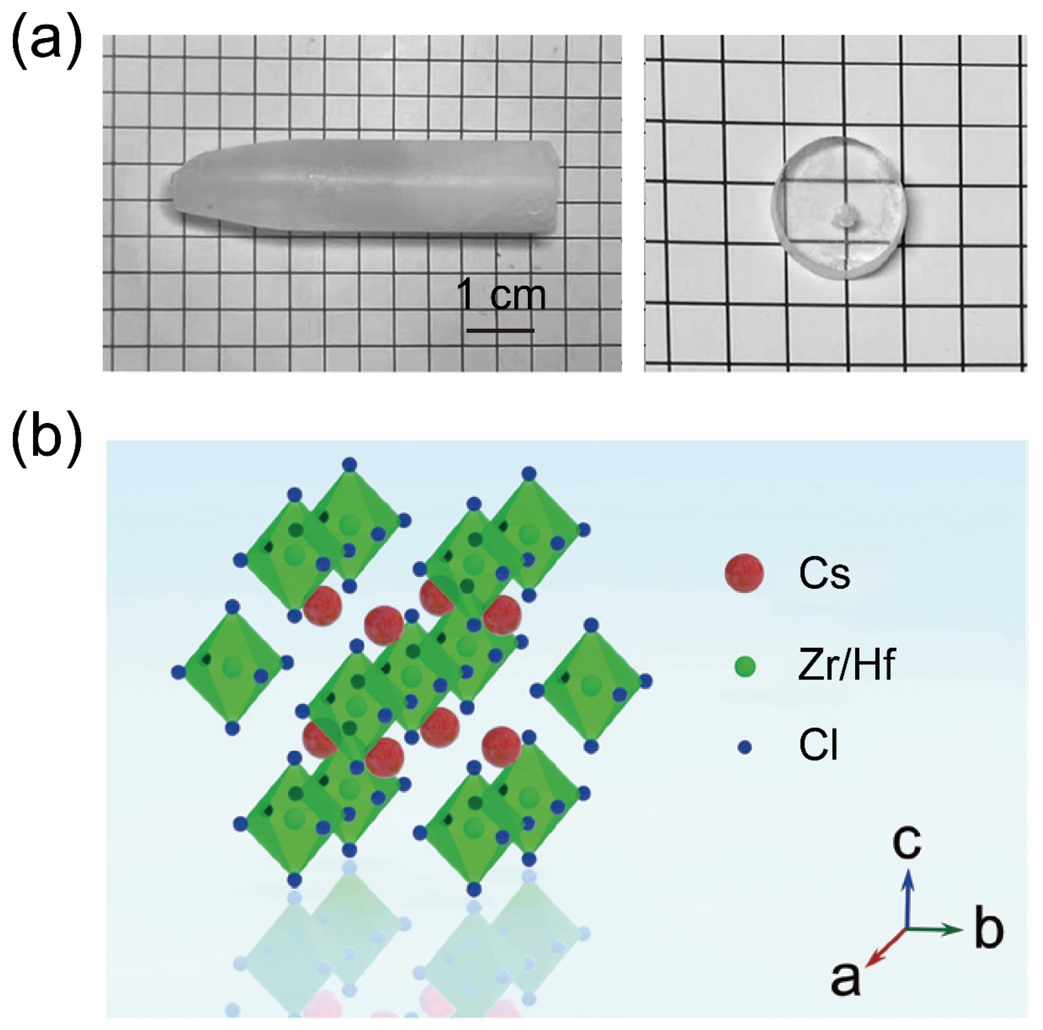
5.3. Zero-Dimensional A2BX6 Perovskite Single Crystals

Zero-dimensional halide perovskites with the A2BX₆ (A = Cs, Rb; B = Hf, Zr, Te, Ti; X = Cl, Br, I) structure represent a distinct class of materials, exhibiting unique physicochemical properties [170,171,172,173,174,175,176,177,178]. These A2BX6 halide perovskites are notable for their lack of extension into higher-dimensional crystal networks. Instead, they exist as isolated molecules or clusters. This structural characteristic leads to highly localized electronic states, which in turn result in exceptional optoelectronic properties, including efficient light absorption and emission. Additionally, in contrast to higher-dimensional metal halide perovskites, A2BX6 perovskites demonstrate superior chemical stability under certain conditions, owing to their more localized structure.
In a recent study, large-scale Cs2ZrCl6:Ce,Li single crystals with exceptional energy resolution were successfully synthesized by optimizing the temperature gradient and growth rate using the Bridgman method, as shown in Figure 12a [179]. Single-crystal diffraction analyses confirm the formation of 0D perovskite structures. Specifically, Zr4+ cations are coordinated with Cl ions to form discrete octahedra, which are isolated by Cs⁺ ions, as depicted in Figure 12b [53]. Further investigations reveal that this effective dual-ion co-substitution strategy makes the Cs2ZrCl6 single crystal an environmentally friendly material, with promising applications in solar-blind ultraviolet optoelectronics and X-ray detection [180,181,182].

6. Conclusions and Perspectives

As a traditional single-crystal growth technique, the Bridgman method has been extensively employed in the preparation of single crystals for a wide range of materials. In the field of metal halide crystal research, the Bridgman method has played a crucial role, significantly advancing both the fundamental understanding and practical applications of halide materials. Based on the metal halide compositions discussed in this review, we summarize the growth parameters of different metal halide single crystals using the Bridgman method, as shown in Table 1.
Up to now, metal halide single crystals grown by the Bridgman method have been widely used in various fields. For example, high-quality CsPbBr3, CsPbCl3, and TlPbI3 single crystals demonstrate high resolution X-ray detection feature [80,94,159]. 6Li-doped Cs3CuI5 single crystals show great potential as scintillator for neutron discrimination [134]. In addition, Er-doped CsCdBr3 single crystals possess unique up conversion capability that can convert low-energy photon to high-energy light, which shows great potential in solar cells [77].
While the Bridgman method offers numerous advantages, it also presents several drawbacks and limitations. One primary disadvantage is the slow cooling process typically employed, which leads to a relatively slow crystal growth rate. As a result, the growth of large single crystals can be time-consuming, potentially increasing production costs. Additionally, although the method allows for precise temperature gradient control, maintaining a stable gradient remains challenging due to factors such as heat conduction, convection, and other operational variables. Furthermore, the Bridgman method may not be suitable for materials with a high thermal expansion coefficient or those prone to volatility. Notably, for materials that require extremely fine structural control, the Bridgman method may lack the necessary precision.
In summary, the Bridgman method for single crystal growth is poised to facilitate the advancement of larger, higher-quality, and higher-performance halide single crystals in future research. This progress will offer substantial support for the application of novel optoelectronic materials, semiconductor materials, and other functional materials. As the process continues to be refined, the Bridgman method will play an increasingly pivotal role in fields such as materials science, energy, and electronic devices.

Funding

This research was funded by Shandong Provincial Natural Science Foundation, grant number ZR2024QE319.

Data Availability Statement

No new data were created or analyzed in this study. Data sharing is not applicable to this article.

Acknowledgments

We would like to express our sincere gratitude to Zhiyan Zhou from the School of Stomatology, Shandong University, for her invaluable assistance with language polishing.

Conflicts of Interest

The authors declare no conflicts of interest.

References

  1. Bisson, P.; Groenzin, H.; Barnett, I.L.; Shultz, M.J. High Yield, Single Crystal Ice via the Bridgman Method. Rev. Sci. Instrum. 2016, 87, 034103. [Google Scholar] [CrossRef] [PubMed]
  2. Derby, J.J.; Yeckel, A. Heat Transfer Analysis and Design for Bulk Crystal Growth: Perspectives on the Bridgman Method. In Handbook of Crystal Growth; Elsevier: Amsterdam, The Netherlands, 2015; pp. 793–843. ISBN 978-0-444-63303-3. [Google Scholar]
  3. Rudolph, P.; Kiessling, F. The Horizontal Bridgman Method. Cryst. Res. Technol. 1988, 23, 1207–1224. [Google Scholar] [CrossRef]
  4. Gaxandet, J.P.; Alboussire, T. Bridgman Growth: Modelling and Experiments. Prog. Cryst. Growth Charact. Mater. 1999, 38, 133–159. [Google Scholar] [CrossRef]
  5. Murugesan, M.; Sidden, C.; Paulraj, R. Growth, Optical and Thermal Properties of Triphenylamine Single Crystal Grown by Modified Vertical Bridgman Method for Optical Application. Solid. State Sci. 2022, 132, 106991. [Google Scholar] [CrossRef]
  6. Fedyushkin, A.I.; Burago, N.G.; Puntus, A.A. Convective Heat and Mass Transfer Modeling under Crystal Growth by Vertical Bridgman Method. J. Phys. Conf. Ser. 2020, 1479, 012029. [Google Scholar] [CrossRef]
  7. Yu, P.; Jiang, B.; Chen, Y.; Zheng, J.; Luan, L. Study on In-Doped CdMgTe Crystals Grown by a Modified Vertical Bridgman Method Using the ACRT Technique. Materials 2019, 12, 4236. [Google Scholar] [CrossRef] [PubMed]
  8. Zhang, P.; Hua, Y.; Li, X.; Zhang, L.; Liu, L.; Li, R.; Zhang, G.; Tao, X. Filter-Free Color Image Sensor Based on CsPbBr3−3n X3n (X = Cl, I) Single Crystals. J. Mater. Chem. C 2021, 9, 2840–2847. [Google Scholar] [CrossRef]
  9. Gille, P.; Mühlberg, M.; Parthier, L.; Rudolph, P. Crystal Growth of PbTe and (Pb, Sn)Te by the Bridgman Method and by THM. Cryst. Res. Technol. 1984, 19, 881–891. [Google Scholar] [CrossRef]
  10. Zhang, G.; Tao, X.; Wang, S.; Shi, Q.; Ruan, H.; Chen, L. Growth Improvement and Quality Evaluation of ZnGeP2 Single Crystals Using Vertical Bridgman Method. J. Cryst. Growth 2012, 352, 67–71. [Google Scholar] [CrossRef]
  11. Wang, C.; Xia, H.; Feng, Z.; Zhang, Z.; Jiang, D.; Gu, X.; Zhang, Y.; Chen, B.; Jiang, H. Infrared Luminescent Properties of Na5Lu9F32 Single Crystals Co-Doped Er3+/Yb3+ Grown by Bridgman Method. J. Alloys Compd. 2016, 686, 816–822. [Google Scholar] [CrossRef]
  12. Mooney, R.P.; McFadden, S.; Gabalcová, Z.; Lapin, J. An Experimental–Numerical Method for Estimating Heat Transfer in a Bridgman Furnace. Appl. Therm. Eng. 2014, 67, 61–71. [Google Scholar] [CrossRef]
  13. He, X.; Li, L.; He, X.; Xie, C. Multi-Physical Field Simulation of Cracking during Crystal Growth by Bridgman Method. Materials 2023, 16, 3260. [Google Scholar] [CrossRef] [PubMed]
  14. Du, Y.; Jie, W.; Wang, T.; Zheng, X.; Xu, Y.; Luan, L. Solution Growth of In-Doped CdMnTe Crystals by the Vertical Bridgman Method with the ACRT Technique. J. Cryst. Growth 2012, 355, 33–37. [Google Scholar] [CrossRef]
  15. Sheng, M.; Wang, S.; Zhu, H.; Liu, Z.; Zhou, G. Computational Applications for the Discovery of Novel Antiperovskites and Chalcogenide Perovskites: A Review. Front. Chem. 2024, 12, 1468434. [Google Scholar] [CrossRef] [PubMed]
  16. Sheng, M.; Zhu, H.; Wang, S.; Liu, Z.; Zhou, G. Accelerated Discovery of Halide Perovskite Materials via Computational Methods: A Review. Nanomaterials 2024, 14, 1167. [Google Scholar] [CrossRef] [PubMed]
  17. Wojakowska, A.; Krzy, E. Phase Diagram for the RbBr–CuBr System. J. Therm. Anal. Calorim. 2011, 65, 491–495. [Google Scholar] [CrossRef]
  18. Kanno, R.; Takeda, Y.; Masuyama, Y.; Yamamoto, O. Phase Diagram and High Copper Ion Conductivity of the Copper(l) Chloride-Rubidium Chloride System. Solid State Ion. 1983, 11, 221–226. [Google Scholar] [CrossRef]
  19. Takahashi, T. Solid-State Ionics—The CuCI-CuI-RbCl System. Solid State Ion. 1981, 3, 283–287. [Google Scholar] [CrossRef]
  20. Malakhovskaya-Rosokha, T.A.; Barchii, I.E.; Pogodin, A.I.; Kokhan, A.P.; Stercho, I.P.; Peresh, E.Y. Interaction of Components in the RbI-CsI-CuI Quasi-Ternary System. Russ. J. Inorg. Chem. 2013, 58, 577–580. [Google Scholar] [CrossRef]
  21. Matsui, T.; Wagner, J.B. Investigations on a High Conductivity Solid Electrolyte System, RbCl + CuCl. J. Electrochem. Soc. 1977, 124, 941–944. [Google Scholar] [CrossRef]
  22. Gut, R.; Iberson, E.; Gruen, D.M. Compounds in the Binary Phase Diagrams of the Monovalent Chlorides with the Multivalent Chlorides; Report number ANL-6803; OSTI ID: 4117130; Argonne National Laboratory: Lemont, IL, USA, 1963. [Google Scholar]
  23. Zhang, P.; Zhang, G.; Liu, L.; Ju, D.; Zhang, L.; Cheng, K.; Tao, X. Anisotropic Optoelectronic Properties of Melt-Grown Bulk CsPbBr3 Single Crystal. J. Phys. Chem. Lett. 2018, 9, 5040–5046. [Google Scholar] [CrossRef] [PubMed]
  24. Yu, X.; Huang, C.; Ni, Y.; Wang, Z.; Wu, H.; Hu, Q.; Liu, G.; Zhou, Q.; Wei, L. Optical Property and Judd-Ofelt Analysis of Dy3+, Na+:PbGa2S4 Crystal Grown by Bridgman Method. J. Lumin. 2023, 262, 119951. [Google Scholar] [CrossRef]
  25. Wang, L.-H.; Chang, L.-S. Thermoelectric Properties of P-Type Ba8Ga16Ge30 Type-I Clathrate Compounds Prepared by the Vertical Bridgman Method. J. Alloys Compd. 2017, 722, 644–650. [Google Scholar] [CrossRef]
  26. Zayachuk, D.M.; Ilyina, O.S.; Pashuk, A.V.; Mikityuk, V.I.; Shlemkevych, V.V.; Csik, A.; Kaczorowski, D. Segregation of the Eu Impurity as Function of Its Concentration in the Melt for Growing of the Lead Telluride Doped Crystals by the Bridgman Method. J. Cryst. Growth 2013, 376, 28–34. [Google Scholar] [CrossRef]
  27. Lai, J.; Zhang, J.; Wang, L.; Min, J.; Wu, W.; Shen, M.; Liang, W. Comparison of Cadmium Manganese Telluride Crystals Grown by Traveling Heater Method and Vertical Bridgman Method. Cryst. Res. Technol. 2015, 50, 817–822. [Google Scholar] [CrossRef]
  28. Xiong, W.; Chen, L.; Huang, L.; Guo, F.; Zhou, Y.; Yuan, H. Bridgman Growth and Characterization of Birefringent Crystal NaNO3. Cryst. Res. Technol. 2015, 50, 250–254. [Google Scholar] [CrossRef]
  29. Jin, M.; Shen, H.; Fan, S.; He, Q.; Xu, J. Industrial Growth and Characterization of Si-doped GaAs Crystal by a Novel Multi-crucible Bridgman Method. Cryst. Res. Technol. 2017, 52, 1700052. [Google Scholar] [CrossRef]
  30. Yang, C.; Wen, Y.; Xiong, J.; Zhou, H.; Pan, S.; Chen, H.; Pan, J. Crystal Growth and Photoelectric Performance of γ-CuCl by the Vertical Bridgman Method. J. Cryst. Growth 2022, 579, 126463. [Google Scholar] [CrossRef]
  31. Gul, R.; Roy, U.N.; Camarda, G.S.; Hossain, A.; Yang, G.; Vanier, P.; Lordi, V.; Varley, J.; James, R.B. A Comparison of Point Defects in Cd1−xZnxTe1−ySey Crystals Grown by Bridgman and Traveling Heater Methods. J. Appl. Phys. 2017, 121, 125705. [Google Scholar] [CrossRef]
  32. Roy, U.N.; Bolotnikov, A.E.; Camarda, G.S.; Cui, Y.; Hossain, A.; Lee, K.; Lee, W.; Tappero, R.; Yang, G.; Gul, R.; et al. High Compositional Homogeneity of CdTexSe1−x Crystals Grown by the Bridgman Method. APL Mater. 2015, 3, 026102. [Google Scholar] [CrossRef]
  33. Colombier, E.; Braithwaite, D. Simple Adaptation of the Bridgman High Pressure Technique for Use with Liquid Media. Rev. Sci. Instrum. 2007, 78, 093903. [Google Scholar] [CrossRef] [PubMed]
  34. Li, L.; Zhang, P.; Li, Z.; Chen, Z. Thermal Field Simulation and Optimization of PbF2 Single Crystal Growth by the Bridgman Method. Crystals 2024, 14, 473. [Google Scholar] [CrossRef]
  35. Zhou, H.; Chen, X.; Zhao, T.; Chen, C.; Han, J.; Pan, S.; Pan, J. Growth and Luminescence Properties of γ-CuBr Single Crystals by the Bridgman Method. CrystEngComm 2023, 25, 1669–1674. [Google Scholar] [CrossRef]
  36. Zayachuk, D.M.; Mikityuk, V.I.; Shlemkevych, V.V.; Kaczorowski, D. Complex Formation and Background Impurity of Oxygen in the PbTe: Eu Doped Crystals Grown from Melt by the Bridgman Method. J. Cryst. Growth 2012, 338, 35–41. [Google Scholar] [CrossRef]
  37. Toufanian, R.; Swain, S.; Becla, P.; Motakef, S.; Datta, A. Cesium Lead Bromide Semiconductor Radiation Detectors: Crystal Growth, Detector Performance and Polarization. J. Mater. Chem. C 2022, 10, 12708–12714. [Google Scholar] [CrossRef]
  38. Dahlen, A.; Fattah, A.; Hanke, G.; Karthaus, E. Bridgman and Czochralski Growth of Ge Si Alloy Crystals. Cryst. Res. Technol. 1994, 29, 187–198. [Google Scholar] [CrossRef]
  39. Kliemt, K.; Krellner, C. Crystal Growth by Bridgman and Czochralski Method of the Ferromagnetic Quantum Critical Material YbNi4P2. J. Cryst. Growth 2016, 449, 129–133. [Google Scholar] [CrossRef]
  40. Hurle, D.T.J. A Mechanism for Twin Formation during Czochralski and Encapsulated Vertical Bridgman Growth of III–V Compound Semiconductors. J. Cryst. Growth 1995, 147, 239–250. [Google Scholar] [CrossRef]
  41. Tonn, J.; Danilewsky, A.N.; Cröll, A.; Matuchova, M.; Maixner, J. Czochralski Growth of Lead Iodide Single Crystals: Investigations and Comparison with the Bridgman Method. J. Cryst. Growth 2011, 318, 558–562. [Google Scholar] [CrossRef]
  42. Akasaka, M.; Iida, T.; Matsumoto, A.; Yamanaka, K.; Takanashi, Y.; Imai, T.; Hamada, N. The Thermoelectric Properties of Bulk Crystalline N- and p-Type Mg2Si Prepared by the Vertical Bridgman Method. J. Appl. Phys. 2008, 104, 013703. [Google Scholar] [CrossRef]
  43. Lyubimova, T.P.; Croell, A.; Dold, P.; Khlybov, O.A.; Fayzrakhmanova, I.S. Time-Dependent Magnetic Field Influence on GaAs Crystal Growth by Vertical Bridgman Method. J. Cryst. Growth 2004, 266, 404–410. [Google Scholar] [CrossRef]
  44. Shimizu, A.; Nishizawa, J.; Oyama, Y.; Suto, K. InP Single Crystal Growth by the Horizontal Bridgman Method under Controlled Phosphorus Vapor Pressure. J. Cryst. Growth 2001, 229, 119–123. [Google Scholar] [CrossRef]
  45. Li, F.; Cabral, M.J.; Xu, B.; Cheng, Z.; Dickey, E.C.; LeBeau, J.M.; Wang, J.; Luo, J.; Taylor, S.; Hackenberger, W.; et al. Giant Piezoelectricity of Sm-Doped Pb(Mg1/3Nb2/3)O3-PbTiO3 Single Crystals. Science 2019, 364, 264–268. [Google Scholar] [CrossRef]
  46. Li, F.; Lin, D.; Chen, Z.; Cheng, Z.; Wang, J.; Li, C.; Xu, Z.; Huang, Q.; Liao, X.; Chen, L.-Q.; et al. Ultrahigh Piezoelectricity in Ferroelectric Ceramics by Design. Nat. Mater. 2018, 17, 349–354. [Google Scholar] [CrossRef]
  47. Qiu, C.; Wang, B.; Zhang, N.; Zhang, S.; Liu, J.; Walker, D.; Wang, Y.; Tian, H.; Shrout, T.R.; Xu, Z.; et al. Transparent Ferroelectric Crystals with Ultrahigh Piezoelectricity. Nature 2020, 577, 350–354. [Google Scholar] [CrossRef] [PubMed]
  48. Chen, H.; Liang, Z.; Luo, L.; Ke, Y.; Shen, Q.; Xia, Z.; Jiang, C.; Pan, J. Bridgman Growth, Crystallographic Characterization and Electrical Properties of Relaxor-Based Ferroelectric Single Crystal PIMNT. J. Alloys Compd. 2012, 518, 63–67. [Google Scholar] [CrossRef]
  49. Liao, F.; Zhao, Y.; Chen, Z.; Zheng, Y.; Chen, H. Bridgman Growth and Photoelectronic Property of Relaxor-Based Ferroelectric Single Crystal Pb(Sm1/2Nb1/2)O3-Pb(Mg1/3Nb2/3)O3-PbTiO3. Crystals 2021, 11, 402. [Google Scholar] [CrossRef]
  50. Liu, Z.; Qin, X.; Liu, X. Luminescence Enrichment in Perovskite-Lanthanide Composites: Complexity and Complementarity. In Handbook on the Physics and Chemistry of Rare Earths; Elsevier: Amsterdam, The Netherlands, 2022; Volume 61, pp. 1–29. ISBN 978-0-323-98594-9. [Google Scholar]
  51. Liu, Z.; Qin, X.; Chen, Q.; Jiang, T.; Chen, Q.; Liu, X. Metal–Halide Perovskite Nanocrystal Superlattice: Self-Assembly and Optical Fingerprints. Adv. Mater. 2023, 35, 2209279. [Google Scholar] [CrossRef] [PubMed]
  52. Chen, Q.; Wu, J.; Ou, X.; Huang, B.; Almutlaq, J.; Zhumekenov, A.A.; Guan, X.; Han, S.; Liang, L.; Yi, Z.; et al. All-Inorganic Perovskite Nanocrystal Scintillators. Nature 2018, 561, 88–93. [Google Scholar] [CrossRef] [PubMed]
  53. Liu, Z.; Qin, X.; Chen, Q.; Chen, Q.; Jing, Y.; Zhou, Z.; Zhao, Y.S.; Chen, J.; Liu, X. Highly Stable Lead-Free Perovskite Single Crystals with NIR Emission Beyond 1100 Nm. Adv. Opt. Mater. 2022, 10, 2201254. [Google Scholar] [CrossRef]
  54. Ma, W.; Qian, Q.; Qaid, S.M.H.; Zhao, S.; Liang, D.; Cai, W.; Zang, Z. Water-Molecule-Induced Reversible Fluorescence in a One-Dimensional Mn-Based Hybrid Halide for Anticounterfeiting and Digital Encryption–Decryption. Nano Lett. 2023, 23, 8932–8939. [Google Scholar] [CrossRef]
  55. Han, T.; Tan, S.; Xue, J.; Meng, L.; Lee, J.; Yang, Y. Interface and Defect Engineering for Metal Halide Perovskite Optoelectronic Devices. Adv. Mater. 2019, 31, 1803515. [Google Scholar] [CrossRef]
  56. Motti, S.G.; Meggiolaro, D.; Martani, S.; Sorrentino, R.; Barker, A.J.; De Angelis, F.; Petrozza, A. Defect Activity in Lead Halide Perovskites. Adv. Mater. 2019, 31, 1901183. [Google Scholar] [CrossRef]
  57. Ono, L.K.; Liu, S.; Qi, Y. Reducing Detrimental Defects for High-Performance Metal Halide Perovskite Solar Cells. Angew. Chem. Int. Ed. 2020, 59, 6676–6698. [Google Scholar] [CrossRef] [PubMed]
  58. Huang, H.; Bodnarchuk, M.I.; Kershaw, S.V.; Kovalenko, M.V.; Rogach, A.L. Lead Halide Perovskite Nanocrystals in the Research Spotlight: Stability and Defect Tolerance. ACS Energy Lett. 2017, 2, 2071–2083. [Google Scholar] [CrossRef]
  59. Yang, F.; Jie, W.; Wang, M.; Sun, X.; Jia, N.; Yin, L.; Zhou, B.; Wang, T. Growth of Single-Crystal Cd0.9Zn0.1Te Ingots Using Pressure Controlled Bridgman Method. Crystals 2020, 10, 261. [Google Scholar] [CrossRef]
  60. Macpherson, S.; Doherty, T.A.S.; Winchester, A.J.; Kosar, S.; Johnstone, D.N.; Chiang, Y.-H.; Galkowski, K.; Anaya, M.; Frohna, K.; Iqbal, A.N.; et al. Local Nanoscale Phase Impurities Are Degradation Sites in Halide Perovskites. Nature 2022, 607, 294–300. [Google Scholar] [CrossRef] [PubMed]
  61. Valueva, A.D.; Novikov, S.A.; Bledsoe, J.; Cai, Y.; Maksimova, A.A.; Locklin, J.; Zhao, Y.; Klepov, V.V. Cubic Halide Perovskites in the Cs(Pb1−xSnx)(Br3−yCly) Solid Solutions for Crack-Free Bridgman Grown Single Crystals. MRS Commun. 2024, 14, 942–948. [Google Scholar] [CrossRef]
  62. Shi, Y.; Zhou, Y.; Ma, Z.; Xiao, G.; Wang, K.; Zou, B. Structural Regulation and Optical Behavior of Three-Dimensional Metal Halide Perovskites under Pressure. J. Mater. Chem. C 2020, 8, 12755–12767. [Google Scholar] [CrossRef]
  63. Wong, W.P.D.; Yin, J.; Chaudhary, B.; Chin, X.Y.; Cortecchia, D.; Lo, S.-Z.A.; Grimsdale, A.C.; Mohammed, O.F.; Lanzani, G.; Soci, C. Large Polaron Self-Trapped States in Three-Dimensional Metal-Halide Perovskites. ACS Mater. Lett. 2020, 2, 20–27. [Google Scholar] [CrossRef]
  64. Huang, X.; Guo, Q.; Kang, S.; Ouyang, T.; Chen, Q.; Liu, X.; Xia, Z.; Yang, Z.; Zhang, Q.; Qiu, J.; et al. Three-Dimensional Laser-Assisted Patterning of Blue-Emissive Metal Halide Perovskite Nanocrystals inside a Glass with Switchable Photoluminescence. ACS Nano 2020, 14, 3150–3158. [Google Scholar] [CrossRef] [PubMed]
  65. Giappa, R.M.; Selivanov, N.I.; Samsonova, A.Y.; Pantousas, A.; Remediakis, I.N.; Kapitonov, Y.V.; Emeline, A.V.; Kopidakis, G.; Stoumpos, C.C. (3-CF3pyH)2(3-CF3Py)Pb3I8: A Three-Dimensional Metal Halide Inorganic Framework with Distinctive Kagomé Bands. Chem. Mater. 2024, 36, 11804–11813. [Google Scholar] [CrossRef]
  66. Krawczyk, R.P.; Hammerl, A.; Schwerdtfeger, P. Coinage Metal Halide Clusters: From Two-Dimensional Ring to Three-Dimensional Solid-State-Like Structures. ChemPhysChem 2006, 7, 2286–2289. [Google Scholar] [CrossRef]
  67. Zhang, W.; Eperon, G.E.; Snaith, H.J. Metal Halide Perovskites for Energy Applications. Nat Energy 2016, 1, 16048. [Google Scholar] [CrossRef]
  68. Lei, L.; Dong, Q.; Gundogdu, K.; So, F. Metal Halide Perovskites for Laser Applications. Adv Funct Mater. 2021, 31, 2010144. [Google Scholar] [CrossRef]
  69. Fu, Y.; Zhu, H.; Chen, J.; Hautzinger, M.P.; Zhu, X.-Y.; Jin, S. Metal Halide Perovskite Nanostructures for Optoelectronic Applications and the Study of Physical Properties. Nat. Rev. Mater. 2019, 4, 169–188. [Google Scholar] [CrossRef]
  70. Stranks, S.D.; Snaith, H.J. Metal-Halide Perovskites for Photovoltaic and Light-Emitting Devices. Nat. Nanotechnol. 2015, 10, 391–402. [Google Scholar] [CrossRef] [PubMed]
  71. Lin, Y.; Pattanasattayavong, P.; Anthopoulos, T.D. Metal-Halide Perovskite Transistors for Printed Electronics: Challenges and Opportunities. Adv. Mater. 2017, 29, 1702838. [Google Scholar] [CrossRef]
  72. Sun, J.; Wu, J.; Tong, X.; Lin, F.; Wang, Y.; Wang, Z.M. Organic/Inorganic Metal Halide Perovskite Optoelectronic Devices beyond Solar Cells. Adv. Sci. 2018, 5, 1700780. [Google Scholar] [CrossRef] [PubMed]
  73. Liu, X.-K.; Xu, W.; Bai, S.; Jin, Y.; Wang, J.; Friend, R.H.; Gao, F. Metal Halide Perovskites for Light-Emitting Diodes. Nat. Mater. 2021, 20, 10–21. [Google Scholar] [CrossRef] [PubMed]
  74. Xiang, W.; Liu, S.; Tress, W. A Review on the Stability of Inorganic Metal Halide Perovskites: Challenges and Opportunities for Stable Solar Cells. Energy Environ. Sci. 2021, 14, 2090–2113. [Google Scholar] [CrossRef]
  75. Cho, H.; Kim, Y.; Wolf, C.; Lee, H.; Lee, T. Improving the Stability of Metal Halide Perovskite Materials and Light-Emitting Diodes. Adv. Mater. 2018, 30, 1704587. [Google Scholar] [CrossRef]
  76. Chen, X.; Wang, Y.; Song, J.; Li, X.; Xu, J.; Zeng, H.; Sun, H. Temperature Dependent Reflectance and Ellipsometry Studies on a CsPbBr3 Single Crystal. J. Phys. Chem. C 2019, 123, 10564–10570. [Google Scholar] [CrossRef]
  77. Cockroft, N.J.; Jones, G.D.; Nguyen, D.C. Dynamics and Spectroscopy of Infrared-to-Visible Upconversion in Erbium-Doped Cesium Cadmium Bromide (CsCdBr3:Er3+). Phys. Rev. B 1992, 45, 5187–5198. [Google Scholar] [CrossRef] [PubMed]
  78. Pilla, O.; Cazzanelli, E.; Blanzat, B.; Andraud, C.; Pelle, F. Comparative Raman Study of Phonon Linewidths in Pure and Lead-Doped CsCdBr3. Phys. Status Solidi (B) 1987, 144, 845–851. [Google Scholar] [CrossRef]
  79. Stoumpos, C.C.; Malliakas, C.D.; Peters, J.A.; Liu, Z.; Sebastian, M.; Im, J.; Chasapis, T.C.; Wibowo, A.C.; Chung, D.Y.; Freeman, A.J.; et al. Crystal Growth of the Perovskite Semiconductor CsPbBr3: A New Material for High-Energy Radiation Detection. Cryst. Growth Des. 2013, 13, 2722–2727. [Google Scholar] [CrossRef]
  80. He, Y.; Matei, L.; Jung, H.J.; McCall, K.M.; Chen, M.; Stoumpos, C.C.; Liu, Z.; Peters, J.A.; Chung, D.Y.; Wessels, B.W.; et al. High Spectral Resolution of Gamma-Rays at Room Temperature by Perovskite CsPbBr3 Single Crystals. Nat. Commun. 2018, 9, 1609. [Google Scholar] [CrossRef] [PubMed]
  81. Dirin, D.N.; Cherniukh, I.; Yakunin, S.; Shynkarenko, Y.; Kovalenko, M.V. Solution-Grown CsPbBr3 Perovskite Single Crystals for Photon Detection. Chem. Mater. 2016, 28, 8470–8474. [Google Scholar] [CrossRef] [PubMed]
  82. Liu, D.; Hu, Z.; Hu, W.; Wangyang, P.; Yu, K.; Wen, M.; Zu, Z.; Liu, J.; Wang, M.; Chen, W.; et al. Two-Step Method for Preparing All-Inorganic CsPbBr3 Perovskite Film and Its Photoelectric Detection Application. Mater. Lett. 2017, 186, 243–246. [Google Scholar] [CrossRef]
  83. Tang, X.; Zu, Z.; Zang, Z.; Hu, Z.; Hu, W.; Yao, Z.; Chen, W.; Li, S.; Han, S.; Zhou, M. CsPbBr3/Reduced Graphene Oxide Nanocomposites and Their Enhanced Photoelectric Detection Application. Sens. Actuators B Chem. 2017, 245, 435–440. [Google Scholar] [CrossRef]
  84. Adinolfi, V.; Yuan, M.; Comin, R.; Thibau, E.S.; Shi, D.; Saidaminov, M.I.; Kanjanaboos, P.; Kopilovic, D.; Hoogland, S.; Lu, Z.; et al. The In-Gap Electronic State Spectrum of Methylammonium Lead Iodide Single-Crystal Perovskites. Adv. Mater. 2016, 28, 3406–3410. [Google Scholar] [CrossRef] [PubMed]
  85. Kang, J.; Wang, L.-W. High Defect Tolerance in Lead Halide Perovskite CsPbBr3. J. Phys. Chem. Lett. 2017, 8, 489–493. [Google Scholar] [CrossRef] [PubMed]
  86. Chen, C.; Fu, Q.; Guo, P.; Chen, H.; Wang, M.; Luo, W.; Zheng, Z. Ionic Transport Characteristics of Large-Size CsPbBr3 Single Crystals. Mater. Res. Express 2019, 6, 115808. [Google Scholar] [CrossRef]
  87. Li, J.; Du, X.; Niu, G.; Xie, H.; Chen, Y.; Yuan, Y.; Gao, Y.; Xiao, H.; Tang, J.; Pan, A.; et al. Rubidium Doping to Enhance Carrier Transport in CsPbBr3 Single Crystals for High-Performance X-Ray Detection. ACS Appl. Mater. Interfaces 2020, 12, 989–996. [Google Scholar] [CrossRef]
  88. Lee, I.Y.; Deleplanque, M.A.; Vetter, K. Developments in Large Gamma-Ray Detector Arrays. Rep. Prog. Phys. 2003, 66, 1095–1144. [Google Scholar] [CrossRef]
  89. Liu, H.; Omura, T.; Watanabe, M.; Yamashita, T. Development of a Depth of Interaction Detector for γ-Rays. Nucl. Instrum. Methods Phys. Res. Sect. A Accel. Spectrometers Detect. Assoc. Equip. 2001, 459, 182–190. [Google Scholar] [CrossRef]
  90. Funk, S. Indirect Detection of Dark Matter with γ Rays. Proc. Natl. Acad. Sci. USA 2015, 112, 12264–12271. [Google Scholar] [CrossRef] [PubMed]
  91. Xu, J.; Maxwell, A.; Wei, M.; Wang, Z.; Chen, B.; Zhu, T.; Sargent, E.H. Defect Tolerance of Mixed B-Site Organic–Inorganic Halide Perovskites. ACS Energy Lett. 2021, 6, 4220–4227. [Google Scholar] [CrossRef]
  92. Smart, T.J.; Takenaka, H.; Pham, T.A.; Tan, L.Z.; Zhang, J.Z.; Ogitsu, T.; Ping, Y. Enhancing Defect Tolerance with Ligands at the Surface of Lead Halide Perovskites. J. Phys. Chem. Lett. 2021, 12, 6299–6304. [Google Scholar] [CrossRef] [PubMed]
  93. Kim, G.; Petrozza, A. Defect Tolerance and Intolerance in Metal-Halide Perovskites. Adv. Energy Mater. 2020, 10, 2001959. [Google Scholar] [CrossRef]
  94. He, Y.; Stoumpos, C.C.; Hadar, I.; Luo, Z.; McCall, K.M.; Liu, Z.; Chung, D.Y.; Wessels, B.W.; Kanatzidis, M.G. Demonstration of Energy-Resolved γ-Ray Detection at Room Temperature by the CsPbCl3 Perovskite Semiconductor. J. Am. Chem. Soc. 2021, 143, 2068–2077. [Google Scholar] [CrossRef] [PubMed]
  95. Cohen, M.I.; Young, K.F.; Chang, T.-T.; Brower, W.S. Phase Transitions in CsPbCl3. J. Appl. Phys. 1971, 42, 5267–5272. [Google Scholar] [CrossRef]
  96. Kobayashi, M.; Omata, K.; Sugimoto, S.; Tamagawa, Y.; Kuroiwa, T.; Asada, H.; Takeuchi, H.; Kondo, S. Scintillation Characteristics of CsPbCl3 Single Crystals. Nucl. Instrum. Methods Phys. Res. Sect. A Accel. Spectrometers Detect. Assoc. Equip. 2008, 592, 369–373. [Google Scholar] [CrossRef]
  97. Balvanz, A.; Bayikadi, K.S.; Liu, Z.; Ie, T.S.; Peters, J.A.; Kanatzidis, M.G. Unveiling the Monoclinic Phase in CsPbBr3−xClx Perovskite Crystals, Phase Transition Suppression and High Energy Resolution γ-Ray Detection. J. Am. Chem. Soc. 2024, 146, 31836–31848. [Google Scholar] [CrossRef] [PubMed]
  98. Liu, F.; Wu, R.; Wei, J.; Nie, W.; Mohite, A.D.; Brovelli, S.; Manna, L.; Li, H. Recent Progress in Halide Perovskite Radiation Detectors for Gamma-Ray Spectroscopy. ACS Energy Lett. 2022, 7, 1066–1085. [Google Scholar] [CrossRef]
  99. Yoon, S.J.; Stamplecoskie, K.G.; Kamat, P.V. How Lead Halide Complex Chemistry Dictates the Composition of Mixed Halide Perovskites. J. Phys. Chem. Lett. 2016, 7, 1368–1373. [Google Scholar] [CrossRef] [PubMed]
  100. Xiao, Z.; Zhao, L.; Tran, N.L.; Lin, Y.L.; Silver, S.H.; Kerner, R.A.; Yao, N.; Kahn, A.; Scholes, G.D.; Rand, B.P. Mixed-Halide Perovskites with Stabilized Bandgaps. Nano Lett. 2017, 17, 6863–6869. [Google Scholar] [CrossRef]
  101. Knight, A.J.; Borchert, J.; Oliver, R.D.J.; Patel, J.B.; Radaelli, P.G.; Snaith, H.J.; Johnston, M.B.; Herz, L.M. Halide Segregation in Mixed-Halide Perovskites: Influence of A-Site Cations. ACS Energy Lett. 2021, 6, 799–808. [Google Scholar] [CrossRef]
  102. Zarick, H.F.; Soetan, N.; Erwin, W.R.; Bardhan, R. Mixed Halide Hybrid Perovskites: A Paradigm Shift in Photovoltaics. J. Mater. Chem. A 2018, 6, 5507–5537. [Google Scholar] [CrossRef]
  103. Nedelcu, G.; Protesescu, L.; Yakunin, S.; Bodnarchuk, M.I.; Grotevent, M.J.; Kovalenko, M.V. Fast Anion-Exchange in Highly Luminescent Nanocrystals of Cesium Lead Halide Perovskites (CsPbX3, X = Cl, Br, I). Nano Lett. 2015, 15, 5635–5640. [Google Scholar] [CrossRef] [PubMed]
  104. Yu, Y.; Zhang, D.; Yang, P. Ruddlesden–Popper Phase in Two-Dimensional Inorganic Halide Perovskites: A Plausible Model and the Supporting Observations. Nano Lett. 2017, 17, 5489–5494. [Google Scholar] [CrossRef]
  105. Pan, D.; Fu, Y.; Spitha, N.; Zhao, Y.; Roy, C.R.; Morrow, D.J.; Kohler, D.D.; Wright, J.C.; Jin, S. Deterministic Fabrication of Arbitrary Vertical Heterostructures of Two-Dimensional Ruddlesden–Popper Halide Perovskites. Nat. Nanotechnol. 2021, 16, 159–165. [Google Scholar] [CrossRef] [PubMed]
  106. Chen, Z.; Guo, Y.; Wertz, E.; Shi, J. Merits and Challenges of Ruddlesden–Popper Soft Halide Perovskites in Electro-Optics and Optoelectronics. Adv. Mater. 2019, 31, 1803514. [Google Scholar] [CrossRef] [PubMed]
  107. Gong, J.; Hao, M.; Zhang, Y.; Liu, M.; Zhou, Y. Layered 2D Halide Perovskites beyond the Ruddlesden–Popper Phase: Tailored Interlayer Chemistries for High-Performance Solar Cells. Angew. Chem. 2022, 134, e202112022. [Google Scholar] [CrossRef]
  108. Chen, Y.; Sun, Y.; Peng, J.; Tang, J.; Zheng, K.; Liang, Z. 2D Ruddlesden–Popper Perovskites for Optoelectronics. Adv. Mater. 2018, 30, 1703487. [Google Scholar] [CrossRef]
  109. Li, J.; Yu, Q.; He, Y.; Stoumpos, C.C.; Niu, G.; Trimarchi, G.G.; Guo, H.; Dong, G.; Wang, D.; Wang, L.; et al. Cs2PbI2Cl2, All-Inorganic Two-Dimensional Ruddlesden–Popper Mixed Halide Perovskite with Optoelectronic Response. J. Am. Chem. Soc. 2018, 140, 11085–11090. [Google Scholar] [CrossRef] [PubMed]
  110. Ruddlesden, S.N.; Popper, P. New Compounds of the K2NIF4 Type. Acta Cryst 1957, 10, 538–539. [Google Scholar] [CrossRef]
  111. Kresse, G.; Furthmüller, J. Efficiency of Ab-Initio Total Energy Calculations for Metals and Semiconductors Using a Plane-Wave Basis Set. Comput. Mater. Sci. 1996, 6, 15–50. [Google Scholar] [CrossRef]
  112. Kresse, G.; Furthmüller, J. Efficient Iterative Schemes for Ab Initio Total-Energy Calculations Using a Plane-Wave Basis Set. Phys. Rev. B 1996, 54, 11169–11186. [Google Scholar] [CrossRef]
  113. Acharyya, P.; Ghosh, T.; Pal, K.; Kundu, K.; Singh Rana, K.; Pandey, J.; Soni, A.; Waghmare, U.V.; Biswas, K. Intrinsically Ultralow Thermal Conductivity in Ruddlesden–Popper 2D Perovskite Cs2PbI2Cl2: Localized Anharmonic Vibrations and Dynamic Octahedral Distortions. J. Am. Chem. Soc. 2020, 142, 15595–15603. [Google Scholar] [CrossRef] [PubMed]
  114. Delaire, O.; Ma, J.; Marty, K.; May, A.F.; McGuire, M.A.; Du, M.-H.; Singh, D.J.; Podlesnyak, A.; Ehlers, G.; Lumsden, M.D.; et al. Giant Anharmonic Phonon Scattering in PbTe. Nat. Mater. 2011, 10, 614–619. [Google Scholar] [CrossRef] [PubMed]
  115. Dissanayake, P.D.; Yeom, K.M.; Sarkar, B.; Alessi, D.S.; Hou, D.; Rinklebe, J.; Noh, J.H.; Ok, Y.S. Environmental Impact of Metal Halide Perovskite Solar Cells and Potential Mitigation Strategies: A Critical Review. Environ. Res. 2023, 219, 115066. [Google Scholar] [CrossRef]
  116. Lyu, M.; Yun, J.; Chen, P.; Hao, M.; Wang, L. Addressing Toxicity of Lead: Progress and Applications of Low-Toxic Metal Halide Perovskites and Their Derivatives. Adv. Energy Mater. 2017, 7, 1602512. [Google Scholar] [CrossRef]
  117. Xiao, Z.; Song, Z.; Yan, Y. From Lead Halide Perovskites to Lead-Free Metal Halide Perovskites and Perovskite Derivatives. Adv. Mater. 2019, 31, 1803792. [Google Scholar] [CrossRef]
  118. Hu, H.; Dong, B.; Zhang, W. Low-Toxic Metal Halide Perovskites: Opportunities and Future Challenges. J. Mater. Chem. A 2017, 5, 11436–11449. [Google Scholar] [CrossRef]
  119. De Souza Carvalho, T.A.; Magalhaes, L.F.; Do Livramento Santos, C.I.; De Freitas, T.A.Z.; Carvalho Vale, B.R.; Vale Da Fonseca, A.F.; Schiavon, M.A. Lead-Free Metal Halide Perovskite Nanocrystals: From Fundamentals to Applications. Chem. Eur. J. 2023, 29, e202202518. [Google Scholar] [CrossRef] [PubMed]
  120. Zhang, L.; Wang, K.; Zou, B. Bismuth Halide Perovskite-Like Materials: Current Opportunities and Challenges. ChemSusChem 2019, 12, 1612–1630. [Google Scholar] [CrossRef]
  121. Ayscue, R.L.; Vallet, V.; Bertke, J.A.; Réal, F.; Knope, K.E. Structure–Property Relationships in Photoluminescent Bismuth Halide Organic Hybrid Materials. Inorg. Chem. 2021, 60, 9727–9744. [Google Scholar] [CrossRef] [PubMed]
  122. Creutz, S.E.; Liu, H.; Kaiser, M.E.; Li, X.; Gamelin, D.R. Structural Diversity in Cesium Bismuth Halide Nanocrystals. Chem. Mater. 2019, 31, 4685–4697. [Google Scholar] [CrossRef]
  123. Li, X.; Du, X.; Zhang, P.; Hua, Y.; Liu, L.; Niu, G.; Zhang, G.; Tang, J.; Tao, X. Lead-Free Halide Perovskite Cs3Bi2Br9 Single Crystals for High-Performance X-Ray Detection. Sci. China Mater. 2021, 64, 1427–1436. [Google Scholar] [CrossRef]
  124. Leng, M.; Yang, Y.; Zeng, K.; Chen, Z.; Tan, Z.; Li, S.; Li, J.; Xu, B.; Li, D.; Hautzinger, M.P.; et al. All-Inorganic Bismuth-Based Perovskite Quantum Dots with Bright Blue Photoluminescence and Excellent Stability. Adv. Funct. Mater. 2018, 28, 1704446. [Google Scholar] [CrossRef]
  125. Bass, K.K.; Estergreen, L.; Savory, C.N.; Buckeridge, J.; Scanlon, D.O.; Djurovich, P.I.; Bradforth, S.E.; Thompson, M.E.; Melot, B.C. Vibronic Structure in Room Temperature Photoluminescence of the Halide Perovskite Cs3Bi2Br9. Inorg. Chem. 2017, 56, 42–45. [Google Scholar] [CrossRef]
  126. Li, X.; Zhang, G.; Hua, Y.; Cui, F.; Sun, X.; Liu, J.; Liu, H.; Bi, Y.; Yue, Z.; Zhai, Z.; et al. Dimensional and Optoelectronic Tuning of Lead-free Perovskite Cs3Bi2I9−nBrn Single Crystals for Enhanced Hard X-ray Detection. Angew. Chem. Int. Ed. 2023, 62, e202315817. [Google Scholar] [CrossRef] [PubMed]
  127. Zhou, Y.; Fei, C.; Uddin, M.A.; Zhao, L.; Ni, Z.; Huang, J. Self-Powered Perovskite Photon-Counting Detectors. Nature 2023, 616, 712–718. [Google Scholar] [CrossRef] [PubMed]
  128. Zhang, X.; Zhu, T.; Ji, C.; Yao, Y.; Luo, J. In Situ Epitaxial Growth of Centimeter-Sized Lead-Free (BA)2CsAgBiBr7/Cs2 AgBiBr6 Heterocrystals for Self-Driven X-Ray Detection. J. Am. Chem. Soc. 2021, 143, 20802–20810. [Google Scholar] [CrossRef]
  129. McCall, K.M.; Stoumpos, C.C.; Kostina, S.S.; Kanatzidis, M.G.; Wessels, B.W. Strong Electron–Phonon Coupling and Self-Trapped Excitons in the Defect Halide Perovskites A3M2I9 (A = Cs, Rb; M = Bi, Sb). Chem. Mater. 2017, 29, 4129–4145. [Google Scholar] [CrossRef]
  130. McCall, K.M.; Liu, Z.; Trimarchi, G.; Stoumpos, C.C.; Lin, W.; He, Y.; Hadar, I.; Kanatzidis, M.G.; Wessels, B.W. α-Particle Detection and Charge Transport Characteristics in the A3M2I9 Defect Perovskites (A = Cs, Rb; M = Bi, Sb). ACS Photonics 2018, 5, 3748–3762. [Google Scholar] [CrossRef]
  131. Lei, X.-W.; Yue, C.-Y.; Zhao, J.-Q.; Han, Y.-F.; Yang, J.-T.; Meng, R.-R.; Gao, C.-S.; Ding, H.; Wang, C.-Y.; Chen, W.-D. Low-Dimensional Hybrid Cuprous Halides Directed by Transition Metal Complex: Syntheses, Crystal Structures, and Photocatalytic Properties. Cryst. Growth Des. 2015, 15, 5416–5426. [Google Scholar] [CrossRef]
  132. Cheng, P.; Sun, L.; Feng, L.; Yang, S.; Yang, Y.; Zheng, D.; Zhao, Y.; Sang, Y.; Zhang, R.; Wei, D.; et al. Colloidal Synthesis and Optical Properties of All-Inorganic Low-Dimensional Cesium Copper Halide Nanocrystals. Angew. Chem. 2019, 131, 16233–16237. [Google Scholar] [CrossRef]
  133. Zhang, P.; Yan, Z.; Li, C.; Du, Y.; Ma, L.; Wang, Z.; Lin, T.; Zhao, L.; Xiao, J. Low-Dimensional Hybrid Copper(I) Halides Single Crystals: Synthesis, Structures, and Tunable Photoluminescence. Chem. Eng. J. 2024, 496, 154106. [Google Scholar] [CrossRef]
  134. Wang, Q.; Wang, C.; Wang, Z.; Sun, X.; Nikl, M.; OuYang, X.; Wu, Y. Achieving Efficient Neutron and Gamma Discrimination in a Highly Stable6 Li-Loaded Cs3Cu2I5 Perovskite Scintillator. J. Phys. Chem. Lett. 2022, 13, 9066–9071. [Google Scholar] [CrossRef] [PubMed]
  135. Liu, D.; Wei, Q.; Tong, Y.; Xiang, P.; Cai, P.; Tang, G.; Shi, H.; Qin, L. A Novel Li+-Doped CsCu2I3 Single Crystal for Dual Gamma–Neutron Detection. CrystEngComm 2023, 25, 58–63. [Google Scholar] [CrossRef]
  136. Combes, C.M.; Dorenbos, P.; Van Eijk, C.W.E.; Krämer, K.W.; Güdel, H.U. Optical and Scintillation Properties of Pure and Ce3+-Doped Cs2LiYCl6 and Li3YCl6:Ce3+ Crystals. J. Lumin. 1999, 82, 299–305. [Google Scholar] [CrossRef]
  137. Glodo, J.; Hawrami, R.; Shah, K.S. Development of Cs2LiYCl6 Scintillator. J. Cryst. Growth 2013, 379, 73–78. [Google Scholar] [CrossRef]
  138. Cheng, S.; Nikl, M.; Beitlerova, A.; Kucerkova, R.; Du, X.; Niu, G.; Jia, Y.; Tang, J.; Ren, G.; Wu, Y. Ultrabright and Highly Efficient All-Inorganic Zero-Dimensional Perovskite Scintillators. Adv. Opt. Mater. 2021, 9, 2100460. [Google Scholar] [CrossRef]
  139. Wang, Q.; Zhou, Q.; Nikl, M.; Xiao, J.; Kucerkova, R.; Beitlerova, A.; Babin, V.; Prusa, P.; Linhart, V.; Wang, J.; et al. Highly Resolved X-Ray Imaging Enabled by In(I) Doped Perovskite-Like Cs3Cu2I5 Single Crystal Scintillator. Adv. Opt. Mater. 2022, 10, 2200304. [Google Scholar] [CrossRef]
  140. Belousov, M.P.; Gromyko, M.V.; Ignatyev, O.V. Scintillation γ Spectrometers for Use at Nuclear Power Plants (Review). Instrum. Exp. Tech. 2017, 60, 1–19. [Google Scholar] [CrossRef]
  141. Dorenbos, P. (INVITED) The Quest for High Resolution γ-Ray Scintillators. Opt. Mater. X 2019, 1, 100021. [Google Scholar] [CrossRef]
  142. Yuan, D. Air-Stable Bulk Halide Single-Crystal Scintillator Cs3Cu2I5 by Melt Growth: Intrinsic and Tl Doped with High Light Yield. ACS Appl. Mater. Interfaces 2020, 12, 38333–38340. [Google Scholar] [CrossRef]
  143. Tsuji, M.; Sasase, M.; Iimura, S.; Kim, J.; Hosono, H. Room-Temperature Solid-State Synthesis of Cs3Cu2I5 Thin Films and Formation Mechanism for Its Unique Local Structure. J. Am. Chem. Soc. 2023, 145, 11650–11658. [Google Scholar] [CrossRef]
  144. Wang, Z.; Wang, L.; Xie, J.; Yang, Y.; Song, Y.; Xiao, G.; Fu, Y.; Zhang, L.; Fang, Y.; Yang, D.; et al. HCOO Doping-Induced Multiexciton Emissions in Cs3Cu2I5 Crystals for Efficient X-Ray Scintillation. Small 2024, 20, 2309922. [Google Scholar] [CrossRef]
  145. Chen, H.; Pina, J.M.; Yuan, F.; Johnston, A.; Ma, D.; Chen, B.; Li, Z.; Dumont, A.; Li, X.; Liu, Y.; et al. Multiple Self-Trapped Emissions in the Lead-Free Halide Cs3 Cu2 I5. J. Phys. Chem. Lett. 2020, 11, 4326–4330. [Google Scholar] [CrossRef] [PubMed]
  146. Lian, L.; Zheng, M.; Zhang, W.; Yin, L.; Du, X.; Zhang, P.; Zhang, X.; Gao, J.; Zhang, D.; Gao, L.; et al. Efficient and Reabsorption-Free Radioluminescence in Cs3Cu2I5 Nanocrystals with Self-Trapped Excitons. Adv. Sci. 2020, 7, 2000195. [Google Scholar] [CrossRef] [PubMed]
  147. Jun, T.; Sim, K.; Iimura, S.; Sasase, M.; Kamioka, H.; Kim, J.; Hosono, H. Lead-Free Highly Efficient Blue-Emitting Cs3Cu2I5 with 0D Electronic Structure. Adv. Mater. 2018, 30, 1804547. [Google Scholar] [CrossRef]
  148. Li, X.; Chen, J.; Yang, D.; Chen, X.; Geng, D.; Jiang, L.; Wu, Y.; Meng, C.; Zeng, H. Mn2+ Induced Significant Improvement and Robust Stability of Radioluminescence in Cs3Cu2I5 for High-Performance Nuclear Battery. Nat. Commun. 2021, 12, 3879. [Google Scholar] [CrossRef] [PubMed]
  149. Heo, J.H.; Shin, D.H.; Park, J.K.; Kim, D.H.; Lee, S.J.; Im, S.H. High-Performance Next-Generation Perovskite Nanocrystal Scintillator for Nondestructive X-Ray Imaging. Adv. Mater. 2018, 30, 1801743. [Google Scholar] [CrossRef]
  150. Van Loef, E.V.; Ciampi, G.; Shirwadkar, U.; Soundara Pandian, L.; Shah, K.S. Crystal Growth and Scintillation Properties of Thallium-Based Halide Scintillators. J. Cryst. Growth 2020, 532, 125438. [Google Scholar] [CrossRef]
  151. Shirwadkar, U.; Loyd, M.; Du, M.-H.; Van Loef, E.; Ciampi, G.; Soundara Pandian, L.; Stand, L.; Koschan, M.; Zhuravleva, M.; Melcher, C.; et al. Thallium-Based Scintillators for High-Resolution Gamma-Ray Spectroscopy: Ce3+-Doped Tl2LaCl5 and Tl2LaBr5. Nucl. Instrum. Methods Phys. Res. Sect. A Accel. Spectrometers Detect. Assoc. Equip. 2020, 962, 163684. [Google Scholar] [CrossRef]
  152. Hawrami, R.; Ariesanti, E.; Buliga, V.; Burger, A. Thallium Strontium Iodide: A High Efficiency Scintillator for Gamma-Ray Detection. Opt. Mater. 2020, 100, 109624. [Google Scholar] [CrossRef]
  153. Kim, H.; Khan, A.; Daniel, J.; Rooh, G.; Vuong, P.Q. Thallium-Based Heavy Inorganic Scintillators: Recent Developments and Future Perspectives. CrystEngComm 2022, 24, 450–464. [Google Scholar] [CrossRef]
  154. Pan, L.; Sholom, S.; McKeever, S.W.S.; Jacobsohn, L.G. Magnesium Aluminate Spinel for Optically Stimulated Luminescence Dosimetry. J. Alloys Compd. 2021, 880, 160503. [Google Scholar] [CrossRef]
  155. Sakai, T.; Koshimizu, M.; Fujimoto, Y.; Nakauchi, D.; Yanagida, T.; Asai, K. Luminescence and Scintillation Properties of Tl- and In-Doped CsCl Crystals. Jpn. J. Appl. Phys. 2017, 56, 062601. [Google Scholar] [CrossRef]
  156. Zazubovich, S.; Voloshinovskii, A.; Stryganyuk, G. Luminescence of CsCl: Tl Crystal under Synchrotron Excitation. Phys. Status Solidi (B) 2002, 233, 238–249. [Google Scholar] [CrossRef]
  157. Nagirnyi, V.; Zazubovich, S.; Jaanson, N. Luminescence of CsCl: Tl Single Crystals. Phys. Status Solidi (B) 1993, 175, 155–164. [Google Scholar] [CrossRef]
  158. Shiran, N.V.; Gektin, A.V.; Boyarintseva, Y.; Vasyukov, S.; Boyarintsev, A.; Pedash, V.; Tkachenko, S.; Zelenskaya, O.; Kosinov, N.; Kisil, O.; et al. Eu Doped and Eu, Tl Co-Doped NaI Scintillators. IEEE Trans. Nucl. Sci. 2010, 57, 1233–1235. [Google Scholar] [CrossRef]
  159. Lin, W.; He, J.; McCall, K.M.; Stoumpos, C.C.; Liu, Z.; Hadar, I.; Das, S.; Wang, H.; Wang, B.; Chung, D.Y.; et al. Inorganic Halide Perovskitoid TlPbI3 for Ionizing Radiation Detection. Adv. Funct. Mater. 2021, 31, 2006635. [Google Scholar] [CrossRef]
  160. Rodi, F.; Babel, D. Ternäre Oxide der Übergangsmetalle. IV. Erdalkaliiridium(IV)-oxide: Kristallstruktur von CalrO3. Z. Anorg Allge Chem. 1965, 336, 17–23. [Google Scholar] [CrossRef]
  161. Li, X.; He, Y.; Kepenekian, M.; Guo, P.; Ke, W.; Even, J.; Katan, C.; Stoumpos, C.C.; Schaller, R.D.; Kanatzidis, M.G. Three-Dimensional Lead Iodide Perovskitoid Hybrids with High X-Ray Photoresponse. J. Am. Chem. Soc. 2020, 142, 6625–6637. [Google Scholar] [CrossRef]
  162. Vtyurina, D.N.; Kaurova, I.A.; Kuz’micheva, G.M.; Rybakov, V.B.; Chernyshov, D.Y.; Khramov, E.V.; Firstov, S.V.; Korchak, V.N. Structural Peculiarities, Point Defects and Luminescence in Bi-Doped CsCdX3 (X = Cl, Br) Single Crystals. J. Alloys Compd. 2019, 803, 912–921. [Google Scholar] [CrossRef]
  163. Vtyurina, D.N.; Eistrikh-Geller, P.A.; Kuz’micheva, G.M.; Rybakov, V.B.; Khramov, E.V.; Kaurova, I.A.; Chernyshov, D.Y.; Korchak, V.N. Influence of Monovalent Bi+ Doping on Real Composition, Point Defects, and Photoluminescence in TlCdCl3 and TlCdI3 Single Crystals. Sci. China Mater. 2017, 60, 1253–1263. [Google Scholar] [CrossRef]
  164. Yang, G.; Phan, Q.V.; Liu, M.; Hawari, A.; Kim, H. Material Defect Study of Thallium Lead Iodide (TlPbI3) Crystals for Radiation Detector Applications. Nucl. Instrum. Methods Phys. Res. Sect. A Accel. Spectrometers Detect. Assoc. Equip. 2020, 954, 161516. [Google Scholar] [CrossRef]
  165. Liu, Z.; Zhang, T.; Wang, Y.; Wang, C.; Zhang, P.; Sarvari, H.; Chen, Z.; Li, S. Electronic Properties of a New All-Inorganic Perovskite TlPbI3 Simulated by the First Principles. Nanoscale Res. Lett. 2017, 12, 232. [Google Scholar] [CrossRef]
  166. Yan, Y.; Liu, F.; Wu, J.; Zhang, Z.; Wu, Z.; Cong, W.-Y.; Guan, C.; Lu, Y.-B. Evaluation of the Electronic Properties of Layered TlPbI3 Perovskites. Phys. B Condens. Matter 2023, 667, 415190. [Google Scholar] [CrossRef]
  167. Khyzhun, O.Y.; Fochuk, P.M.; Kityk, I.V.; Piasecki, M.; Levkovets, S.I.; Fedorchuk, A.O.; Parasyuk, O.V. Single Crystal Growth and Electronic Structure of TlPbI3. Mater. Chem. Phys. 2016, 172, 165–172. [Google Scholar] [CrossRef]
  168. Lin, W.; Stoumpos, C.C.; Liu, Z.; Das, S.; Kontsevoi, O.Y.; He, Y.; Malliakas, C.D.; Chen, H.; Wessels, B.W.; Kanatzidis, M.G. TlSn2I5, a Robust Halide Antiperovskite Semiconductor for γ-Ray Detection at Room Temperature. ACS Photonics 2017, 4, 1805–1813. [Google Scholar] [CrossRef]
  169. Li, W.; Li, M.; He, Y.; Song, J.; Guo, K.; Pan, W.; Wei, H. Arising 2D Perovskites for Ionizing Radiation Detection. Adv. Mater. 2024, 36, 2309588. [Google Scholar] [CrossRef] [PubMed]
  170. Ni, Z.; Zhao, J.; Zhang, G.; Chen, Y.; Lian, H.; Lin, J. Synthesis of Pb-free Double-Perovskite Heterojunction (Cs2SnCl6-Bi3+&Te4+/Cs2GeF6-Mn4+) with White Emission for LED Application. Adv. Opt. Mater. 2023, 11, 2203029. [Google Scholar] [CrossRef]
  171. Zhou, J.; Luo, J.; Rong, X.; Wei, P.; Molokeev, M.S.; Huang, Y.; Zhao, J.; Liu, Q.; Zhang, X.; Tang, J.; et al. Lead-Free Perovskite Derivative Cs2 SnCl6−xBrxSingle Crystals for Narrowband Photodetectors. Adv. Opt. Mater. 2019, 7, 1900139. [Google Scholar] [CrossRef]
  172. Sun, J.; Zheng, W.; Huang, P.; Zhang, M.; Zhang, W.; Deng, Z.; Yu, S.; Jin, M.; Chen, X. Efficient Near-Infrared Luminescence in Lanthanide-Doped Vacancy-Ordered Double Perovskite Cs2ZrCl6 Phosphors via Te4+ Sensitization. Angew. Chem. Int. Ed. 2022, 61, e202201993. [Google Scholar] [CrossRef]
  173. Wang, A.; Yan, X.; Zhang, M.; Sun, S.; Yang, M.; Shen, W.; Pan, X.; Wang, P.; Deng, Z. Controlled Synthesis of Lead-Free and Stable Perovskite Derivative Cs2SnI6 Nanocrystals via a Facile Hot-Injection Process. Chem. Mater. 2016, 28, 8132–8140. [Google Scholar] [CrossRef]
  174. Scott, S.M.; Zhu, W.; Yao, T.; Vienna, J.D.; Ewing, R.C.; Lian, J. The Thermal Stability and Consolidation of Perovskite Variant Cs2SnCl6 Using Spark Plasma Sintering. J. Am. Ceram. Soc. 2018, 101, 2060–2065. [Google Scholar] [CrossRef]
  175. Chang, T.; Wei, Q.; Zeng, R.; Cao, S.; Zhao, J.; Zou, B. Efficient Energy Transfer in Te4+-Doped Cs2ZrCl6 Vacancy-Ordered Perovskites and Ultrahigh Moisture Stability via A-Site Rb-Alloying Strategy. J. Phys. Chem. Lett. 2021, 12, 1829–1837. [Google Scholar] [CrossRef] [PubMed]
  176. Qing, X.; Wu, C.; Han, X. Efficient Near-Infrared Luminescence Based on Double Perovskite Cs2SnCl6. Molecules 2023, 28, 3593. [Google Scholar] [CrossRef] [PubMed]
  177. Jin, M.; Zheng, W.; Gong, Z.; Huang, P.; Li, R.; Xu, J.; Cheng, X.; Zhang, W.; Chen, X. Unraveling the Triplet Excited-State Dynamics of Bi3+ in Vacancy-Ordered Double Perovskite Cs2SnCl6 Nanocrystals. Nano Res. 2022, 15, 6422–6429. [Google Scholar] [CrossRef]
  178. Das Adhikari, S.; Echeverría-Arrondo, C.; Sánchez, R.S.; Chirvony, V.S.; Martínez-Pastor, J.P.; Agouram, S.; Muñoz-Sanjosé, V.; Mora-Seró, I. White Light Emission from Lead-Free Mixed-Cation Doped Cs2SnCl6 Nanocrystals. Nanoscale 2022, 14, 1468–1479. [Google Scholar] [CrossRef] [PubMed]
  179. Jia, X.; Wang, B.; Zhu, M.; Zhang, Y.; Chong, X.; Li, J.; Wang, J. Growth Process and Optical Properties of Cs2ZrCl6 Doped with Ce3+ and Li+ Crystals. Cryst. Growth Des. 2023, 23, 3589–3594. [Google Scholar] [CrossRef]
  180. Buryi, M.; Babin, V.; Ligthart, R.A.M.; Nagorny, S.S.; Mikhailik, V.B.; Vaněček, V.; Prouzová Prochazková, L.; Kandel, R.; Nahorna, V.V.; Wang, P. Correlation of Emission, Scintillation and Charge Trapping Properties in Cs2HfCl6 and Cs2ZrCl6 Single Crystals. J. Mater. Chem. C 2021, 9, 2955–2968. [Google Scholar] [CrossRef]
  181. Vanecek, V.; Kral, R.; Paterek, J.; Babin, V.; Jary, V.; Hybler, J.; Kodama, S.; Kurosawa, S.; Yokota, Y.; Yoshikawa, A.; et al. Modified Vertical Bridgman Method: Time and Cost Effective Tool for Preparation of Cs2HfCl6 Single Crystals. J. Cryst. Growth 2020, 533, 125479. [Google Scholar] [CrossRef]
  182. Jia, X.; Jiang, H.; Chong, X.; Ju, W.; Feng, T.; Zhao, Z.; Wei, H.; Li, J.; Cheng, S.; Wang, J. A Novel Co-Substitution Strategy for the Design, Growth, and Optoelectronic Performance Optimization of Cs2ZrCl6:Ce,Li Single Crystals. J. Mater. Chem. C 2025, 13, 2844–2852. [Google Scholar] [CrossRef]
  183. Song, J.; Cui, Q.; Li, J.; Xu, J.; Wang, Y.; Xu, L.; Xue, J.; Dong, Y.; Tian, T.; Sun, H.; et al. Ultralarge All-Inorganic Perovskite Bulk Single Crystal for High-Performance Visible–Infrared Dual-Modal Photodetectors. Adv. Opt. Mater. 2017, 5, 1700157. [Google Scholar] [CrossRef]
Figure 2. (a) Phase transitions in CsPbBr3, during which the PbBr6 octahedra exhibit distortion. (b) Photos of as-prepared large-sized CsPbBr3 single crystal. Bottom pictures are the single crystal wafers of different sizes. (c) HRTEM picture of 3D CsPbBr3 single crystal. (d) The corresponding SAED pattern and (e) magnified lattice image. The yellow box is drawn to compare HRTEM image. Reprinted with permission from Ref. [80]. Copyright 2018, Nature Publishing Group.
Inorganics 13 00053 g002
Figure 3. (a) Pictures of large-sized CsPbBr3 single crystals (top), cut wafer (bottom left), and cuboid CsPbBr3 single crystals (bottom right). (b) Responsivity and EQE for the three crystallographic planes. (c) Dark current–voltage features of CsPbBr3 single crystals. Reprinted with permission from Ref. [23]. Copyright 2018, American Chemical Society.
Inorganics 13 00053 g003
Figure 4. (a) Structural evolution of CsPbCl3 near ambient temperature. (b) Photograph of CsPbCl3 single crystal grown by the Bridgman method and (c) its optical transmission. Reprinted with permission from Ref. [94]. Copyright 2021, American Chemical Society.
Inorganics 13 00053 g004
Figure 5. (a) Photographs of CsPbBr3−3nX3n single crystals with mixed halogens and (b) their corresponding UV–Vis absorption spectra. Reprinted with permission from Ref. [8]. Copyright 2021, Royal Society of Chemistry.
Inorganics 13 00053 g005
Figure 6. (a) Picture of Cs2PbI2Cl2 single crystal grown using the Bridgman method. Crystal structure of Cs2PbI2Cl2, shown from (b) the side view and (c) the top-down view. Additionally, (d) depicts the elongated [PbI2Cl4]4− octahedral unit. Reprinted with permission from Ref. [109]. Copyright 2018, American Chemical Society.
Inorganics 13 00053 g006
Figure 7. (a) Picture of Cs2PbI2Cl2 single crystals prepared by the Bridgman method. (b) Crystal structure of the 2D RP metal halide Cs2PbI2Cl2. Reprinted with permission from Ref. [113]. Copyright 2020, American Chemical Society.
Inorganics 13 00053 g007
Figure 8. (a) Schematic illustration of the Bridgman method used for the synthesis of Cs3Bi2Br9 single crystals. (b) The optimized thermal profile. (c) Pictures of Cs3Bi2Br9-1 (top) and Cs3Bi2Br9-2 (bottom). (d) Transmission spectra of Cs3Bi2Br9-1 and Cs3Bi2Br9-2. Insets show the oriented (−1 2 0) planes of these two single crystals. (e) Crystal structure of Cs3Bi2Br9. Reprinted with permission from Ref. [123]. Copyright 2021, Science China Press.
Inorganics 13 00053 g008
Figure 9. (a) Photographs of as-grown Cs3Bi2I9-nBrn single crystals and their corresponding (001)-oriented plates. (b) Comparison of sensitivities between Pb-free perovskite single crystals, commercial CdZnTe single crystals, and commercial α-Se. Reprinted with permission from Ref. [126]. Copyright 2023, Wiley-VCH GmBH. (c) Temperature-dependent photoluminescence spectra of Cs3Sb2I9 at 5 mW excitation power. (d) Temperature-dependent FWHM fitted using H-S equation. Reprinted with permission from Ref. [129]. Copyright 2017, American Chemical Society.
Inorganics 13 00053 g009
Figure 10. (a) As-grown Cs3Cu2I5:6Li crystal ingot with a 7 mm diameter (top) and polished Cs3Cu2I5 (bottom left) and Cs3Cu2I5:6Li (bottom right) slabs. (b) PSD scatter plot and one-dimensional histogram of a Cs3Cu2I5:6Li single crystal upon excitation with a 252Cf source and a 137Cs source. Reprinted with permission from Ref. [134]. Copyright 2022, American Chemical Society. (c) As-grown 7 mm diameter Tl-doped Cs3Cu2I5 crystal ingot, and a 1 mm thick sample under daylight and ultraviolet light. (d) Comparison of absolute light yield between Tl-doped Cs3Cu2I5:Tl, undoped Cs3Cu2I5, and other conventional scintillators. Reprinted with permission from Ref. [138]. Copyright 2021, Wiley-VCH GmBH. (e) Cs3Cu2I5:In crystal slabs under daylight, 254 nm, and 365 nm UV light illumination. (f) X-ray 2D spatial images of the test-pattern plate using 0.2% In-doped Cs3Cu2I5 single crystals. Reprinted with permission from Ref. [139]. Copyright 2022, Wiley-VCH GmBH.
Inorganics 13 00053 g010
Figure 12. (a) As-grown Cs2ZrCl6:Ce,Li single crystal (left) and its wafer (right). Reprinted with permission from Ref. [179]. Copyright 2023, American Chemical Society. (b) Atomic structure of 0D perovskite crystal. Reprinted with permission from Ref. [53]. Copyright 2022, Wiley-VCH GmbH.
Inorganics 13 00053 g012
Table 1. Growth parameters of metal halide single crystals using the Bridgman method.
MaterialsSubstanceTemperature Gradient (°C/cm)Growth RateReferences
CsPbX3CsX, PbX210–300.2–1 mm/hour[8]
CsPbBr3CsBr, PbBr230–401 mm/hour[23]
CsPbBr3CsBr, PbBr250–700.2–0.6 mm/hour[76,183]
CsPbBr3CsBr, PbBr25–200.5–2 mm/hour[80]
CsPbCl3CsCl, PbCl25–200.1–1 mm/hour[94]
γ-CuClCuCl208 mm/day[30]
γ-CuBrCuBr56 mm/day[35]
CsPbBr3CsBr, PbBr2103–30 mm/hour[79]
PbI2PbI2220.5–1.0 mm/hour[41]
TlSn2I5Sn, I2, TlI23 [168]
Tl2HfX6TlX, HfX4/0.2–1 mm/hour[150]
Tl2LaX5TlX, LaX3/0.2–1 mm/hour[150]
A3M2I9 (A = Cs, Rb; M = Bi, Sb)Cs3Sb2I9: Sb2O3, HI, Cs2CO3;
Cs3Bi2I9: Bi2O3, HI, CsI;
Rb3Bi2I9: BiI3, RbI
/2 mm/hour[129,130]
TlPbI3TlI, PbI21220 mm/day[167]
TlPbI3Tl, Pb, I280.5 mm/hour[159]
Eu-doped TlSr2I5TlI, SrI2, EuI2/10 mm/day[152]
Bi-doped CsCdX3CsX, CdX2, BiX3/2 mm/hour[162]
Sn-doped CsPbX3CsX, PbX2, SnX2/1.4 mm/hour[61]
Bi-doped TlCdCl3TlCl, CdCl2, BiCl3/1 mm/hour[163]
Cs2PbI2Cl2CsI, PbCl2/0.7 mm/hour[109]
Cs2PbI2Cl2CsI, PbCl2/0.77 mm/hour[113]
Cs3Bi2Br9CsBr, BiBr310–200.5–3.0 mm/hour[123]
Cs3Bi2I8BrCsI, BiBr3151 mm/hour[126]
6Li-doped Cs3Cu2I5CsI, CuI, 6LiI/0.4 mm/hour[134]
Tl-doped Cs3Cu2I5CsI, CuI, TlI20–300.5–1.0 mm/hour[138]
Ce,Li-doped Cs2ZrCl6CsCl, ZrCl4, CeCl3, LiCl150.7 cm/day[179]
Disclaimer/Publisher’s Note: The statements, opinions and data contained in all publications are solely those of the individual author(s) and contributor(s) and not of MDPI and/or the editor(s). MDPI and/or the editor(s) disclaim responsibility for any injury to people or property resulting from any ideas, methods, instructions or products referred to in the content.

