Article

Design, Construction and Programming of a Low-Cost Pulsed High-Voltage Direct Current Power Supply for the Electrophoretic Deposition of Silicon Carbide Mixed with Graphite and/or Alumina for Thermoelectric Applications

by
Juan Jesús Reyes Valdez
1,
Edna Carina De la Cruz Terrazas
2 and
Eugenio Rodríguez González
1,*
1
Instituto Politécnico Nacional-Centro de Investigación en Ciencia Aplicada y Tecnología Avanzada, Unidad Altamira, Carretera Tampico-Puerto Industrial Altamira Km. 14.5, Altamira 89600, Tamaulipas, Mexico
2
Consejo Nacional de Humanidades, Ciencias y Tecnologías (CONAHCYT), Instituto Politécnico Nacional-Centro de Investigación en Ciencia Aplicada y Tecnología Avanzada, Unidad Altamira, Carretera Tampico-Puerto Industrial Altamira Km. 14.5, Altamira 89600, Tamaulipas, Mexico
*
Author to whom correspondence should be addressed.
Inventions 2024, 9(2), 40; https://doi.org/10.3390/inventions9020040
Submission received: 19 February 2024 / Revised: 4 April 2024 / Accepted: 8 April 2024 / Published: 12 April 2024
(This article belongs to the Section Inventions and Innovation in Applied Chemistry and Physics)

Abstract

:
This document describes a proprietary design, construction, programming and testing of a low-cost pulsed high-voltage direct current (HVDC) power supply with an output of 430 V and power of 25 W. The design obtained allows costs to be reduced compared to commercial ones, highlighting that the manufacturing of this HVDC is easy to replicate. To demonstrate the operation of the pulsed power supply prototype, coatings of silicon carbide (SiC) and SiC mixed with graphite (C) and/or alumina (Al2O3) were made using the electrophoretic deposition (EPD) method. After processing, samples underwent a heat treatment at 500 °C to evaluate their thermoelectric (TE) efficiency. The samples were analysed via X-ray diffraction (XRD), scanning electron microscopy (SEM), Raman spectroscopy, Seebeck coefficient, electrical conductivity and thermal conductivity. The Seebeck coefficient, electrical conductivity and thermal conductivity were measured in a temperature range of 100–500 °C in a nitrogen (N2) atmosphere. The electrical conductivity of the SiC 6C-4Al sample was 0.65 S/cm at 500 °C, while the maximum Seebeck coefficient was 2500 μV/K of the SiC 6C-4Al sample at 200 °C. The thermal conductivity of SiC 6C-4Al was in the range of 0.35–0.37 W/m·K, which was much lower than the SiC sample free of alumina and graphite in the same measured temperature range. In conclusion, the SiC 6C-4Al sample presented the highest figure of merit with a ZT ≈ 0.01.

1. Introduction

The design and construction of an HVDC power supply for high voltage generation can be performed using multiple methods, such as the Cockroft–Walton voltage multiplier [1,2], Dickson voltage multiplier [3,4], Delon charge pump circuit [5,6] half-wave and full-wave voltage doubler [7,8], as well as voltage triples and quadruples [9], and so on. Voltage multiplier circuits are essential components in various research and technology devices, including HVDC generation. These circuits utilize diodes and a capacitor to produce a direct current (DC) output voltage that is multiple times higher than the maximum peak value of the alternating current (AC) input voltage. To provide an increase in voltage, first, a voltage inversion stage is built, followed by a voltage multiplying stage, and finally a load control stage. Figure 1 shows a diagram of the HVDC generation through the inverting and voltage multiplication circuit.
In this way, the electrophoretic technique can be used to create coatings by applying high voltage between two electrodes. EPD is a useful method for processing materials, particularly coatings and nanostructures. It involves moving charged particles in a colloidal suspension through a solvent by applying an electric field and then depositing the material on an oppositely charged conductive substrate [10,11]. The advantage of EPD allows for the production of an extensive range of structures with complex geometries, and films of variable thicknesses from nanometric to a fraction of a millimetre and from porous scaffolds to greatly compact coatings with a low-cost process and simple set up [11,12]. Additionally, these commercial devices are usually quite expensive. For this reason, voltage quadruple circuits with charge control are an alternative to increasing the output voltage since they present the advantages of low cost and easy construction and can be used for coating applications by EDP. On the other hand, the increasing demand for energy, together with the drastic changes in the climate due to the use of fossil fuels for transport and energy generation, has made it necessary to boost research on newer and renewable energy that will be essential for resolving the power crisis in the future [13]. TE devices can use thermal sources, like solar energy and industrial waste heat, to directly transform heat into electrical energy [14]. Since thermoelectric materials can provide answers to the aforementioned issues, they can play an important role in the development of sustainable and renewable energy-harvesting technologies [15]. The efficiency of TE materials is determined by the material’s dimensionless figure of merit, ZT, defined by
Z T = S 2 σ κ L + κ e T
where S is the Seebeck coefficient (µV/K), σ is the electrical conductivity (S/cm), T is the absolute temperature (Kelvin, K) and κL and κe are the lattice and electronic thermal conductivities (W/m·K), respectively [14]. Reducing the total thermal conductivity and increasing the power factor (PF, described in Equation (2)) are the two general approaches for improving the efficiency of TE materials [15].
P F = S 2 σ
High temperatures have significant potential for heat recovery, making high-temperature TE materials extremely important in industrial applications [16]. Three types of commonly used high-temperature TE materials include Si-Ge alloys, half-Heusler (HH) and skutterudites [17]. The research on substitute thermoelectric materials that do not contain expensive and/or rare elements is crucial because these materials contain expensive and toxic elements [18]. Due to their high Seebeck coefficient and high temperature stability as refractory materials, carbide ceramics, such as SiC, provide an economical substitute for these materials as high-temperature TE materials [19]. Semiconductor compounds, such as Bi2Te3, PbTe and their solid solutions, have already been commercially applied to both refrigeration and power generation. However, these materials so far developed are easily oxidized, decomposed or melt above 1000 °C and consequently are not suitable for high-temperature applications [20]. Furthermore, tellurium is scarce on earth, toxic and a volatile element at high temperatures, so its use is limited [21]. Conversely, silicon carbide exhibits mechanical, chemical and thermal stability at high temperatures. Despite these advantages, the high thermal conductivity and electrical resistivity of SiC reduce its TE efficiency, requiring the use of electrically conductive materials and strict control of production conditions to improve its TE potential [22]. SiC is a promising TE material as it is composed of earth-abundant components and has a wide scope for phase optimization, although its ZT values are minimal compared to widely used TE materials [23]. As stated above, increasing the σ and reducing the total thermal conductivity ( κ T = κ L + κ E ) of SiC are crucial to improve its TE performance. In this sense, the addition of graphite can increase electrical conductivity [24], and the addition of alumina can help reduce thermal conductivity [25] to increase thermoelectric efficiency. Therefore, the objective of this work was to build our own prototype of a low-cost power supply to process coatings using the electrophoretic deposition method with economical, non-toxic materials and high-temperature resistant materials. To achieve this purpose, SiC was deposited with the addition of alumina and graphite powders in different concentrations and thermally treated at 500 °C. The structural, electrical and thermal properties that affect the thermoelectric efficiency of SiC were investigated.

2. Materials and Methods

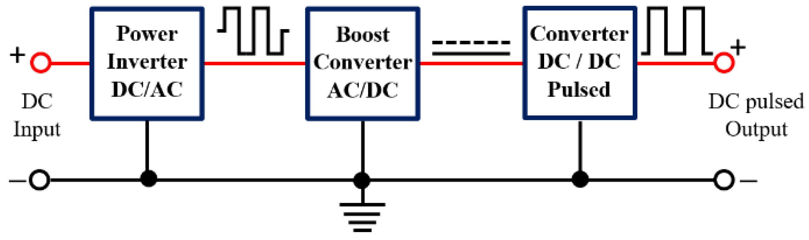
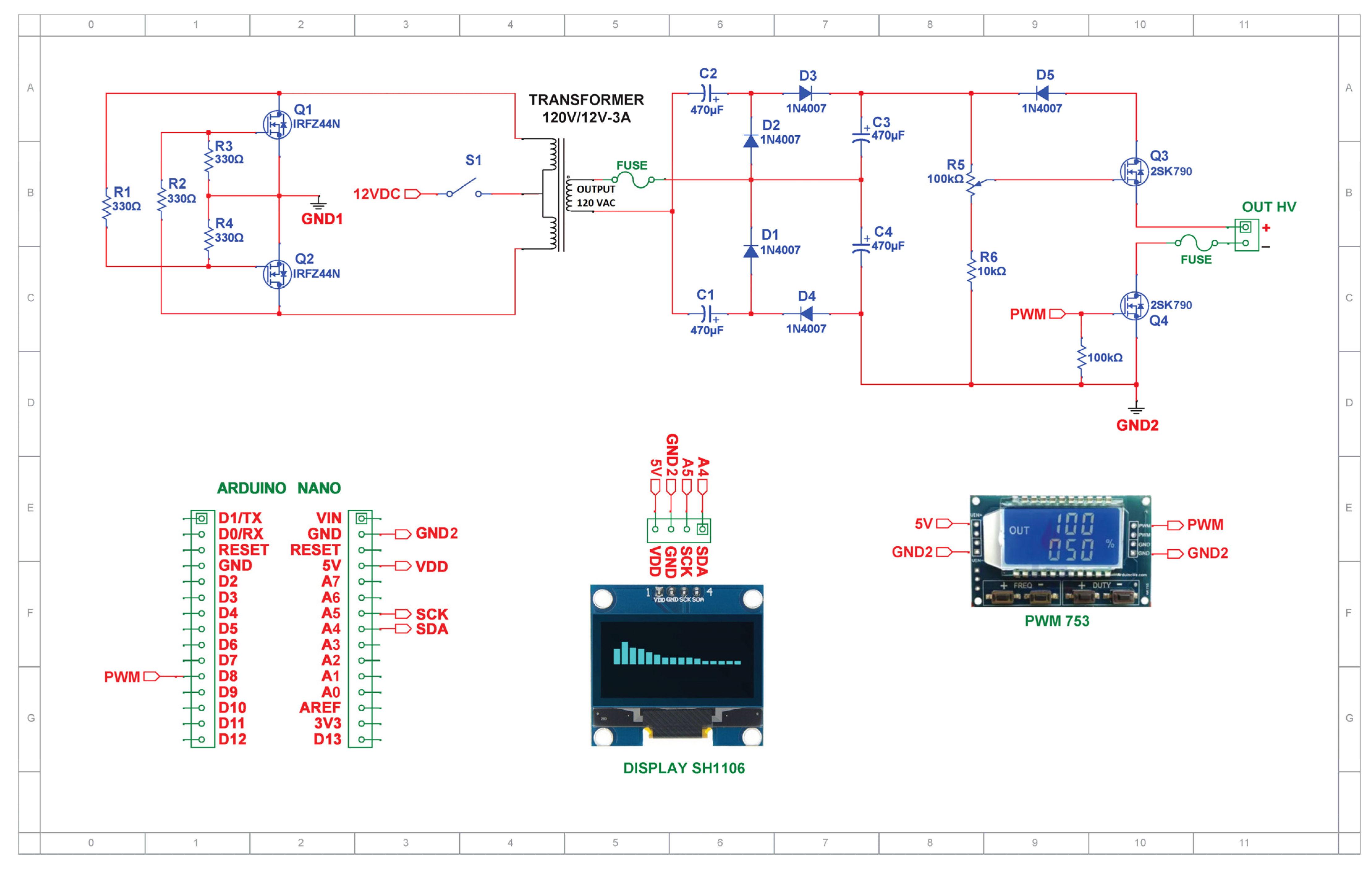
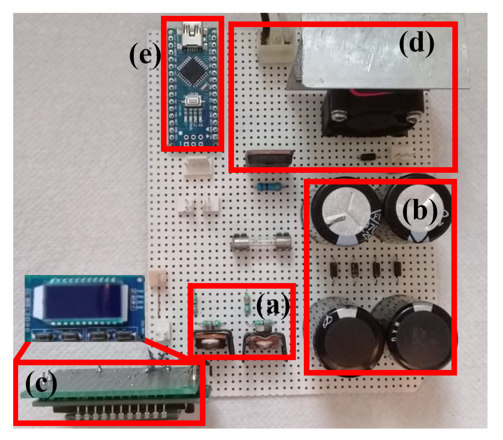
2.1. Experimental Hardware Configuration

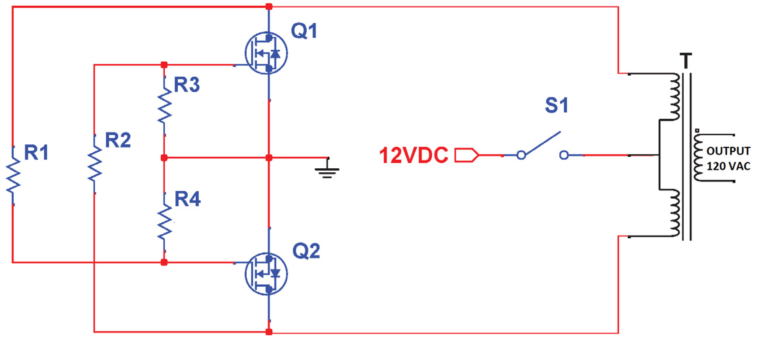
2.1.1. Voltage Inverter

A voltage inverter is a key component in the electrical power system. Adjustable speed drives [26], uninterruptible power supplies [27], electric vehicles [28] and the integration of renewable energy generation in power systems [29] are some areas where voltage inverters are deployed. There are different types of voltage inverters on the market, but these are expensive, and the circuits are complex. Hence, for the construction of an HVDC, the first stage consists of a voltage inverter that is simple to manufacture and inexpensive. Its main components are a centre-tapped transformer (T), two power MOSFETs (Q1, Q2), four resistors (R1–R4) and a DC power supply (12 V/1.25 A) as shown in Figure 2.
Although shown as a saturable core oscillator, no independent feedback windings are employed. Rather, the feedback is generated by cross-coupled connections in the manner of a multivibrator. At full load, the efficiency is close to ~75 percent. In this type of circuit, efficiency, frequency, the output voltage and starting capacity are interdependent. For this reason, the values of the resistors are the same because if the value of a resistor changes, the biasing networks of the two MOSFETs will not be in equilibrium and there will be unequal heat dissipation in the transistors, an asymmetric waveform between other malfunctions. The operation of this voltage inverter is that of a cross-coupled multivibrator; that is, each half of the primary transformer is alternately switched through the 12 V voltage input. When the switch S1 is closed and power is applied, both MOSFETs will receive bias and therefore turn on through the resistors of R1 and R2. However, due to slight differences in components, one MOSFET will turn on before the other. That is, MOSFET Q1 will turn on first. The upper half of the transformer winding will now have current flowing, which induces an opposite current flow in the lower half of the winding. As the MOSFET Q1 receives its bias from the bottom winding via R2, this is now reversed, and the MOSFET Q1 is turned off. The MOSFET Q2 now turns on because R1 is now powered from the 12 V input voltage through the upper half of the transformer winding. The R3, R4 gate resistors ensure that the MOSFETs are turned off when they should be. The frequency will depend on the characteristics of the transformer, which is normally around 50–60 Hz.

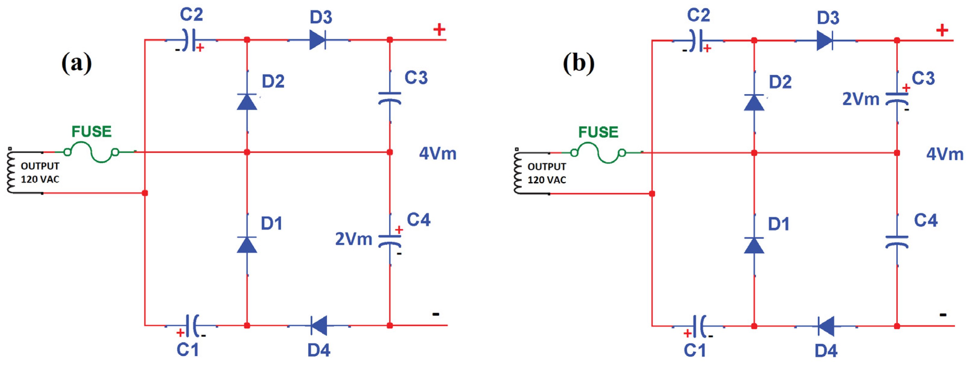
2.1.2. Voltage Quadruple

By boosting the peak voltage to two, three, four or more times the rectified peak voltage, voltage multiplier circuits can generate a relatively large peak voltage with a very low power capacity [7]. A voltage quadruple circuit, as seen in Figure 3, produces a DC output voltage that is four times the primary AC voltage peak value. During the primary transformer’s positive half-cycle, the capacitor C2 charges through diode D2 to peak voltage (Vm). Additionally, if the capacitance values of the capacitors are the same, capacitor C1 charges to Vm trough diode D4. It is worth mention that capacitor C1 charges to Vm with the opposite polarity compared to C2. Figure 3a displays the charging voltage and polarities of capacitors C1 and C2, at this half-cycle. In the negative half-cycle of the input transformer voltage, C3 charges through D3 and the voltage of C2 adds with that of the transformer, thus charging C3 to 2 Vm through D3 and discharging C2 in the process. In a quite similar way to the previous step, during this half-cycle, C4 charges through D1 and the voltage across C1 adds with that of the transformer, thus charging C4 to 2 Vm through D1 and discharging C1 in the process. The charging voltages and polarities of capacitors C3 and C4, at this half-cycle, are depicted in Figure 3b. At this point, the output voltage across C3 and C4 is 4 Vm. During the ensuing positive half-cycle, the charge on capacitors C2, C1 is replenished. The charge on C4 and C3 is replenished by the subsequent negative cycle. The voltage rating of C1 and C2 must be greater than Vm, while that of C3 and C4 must be greater than 2 Vm. Every diode needs to have a voltage rating greater than 4 Vm.

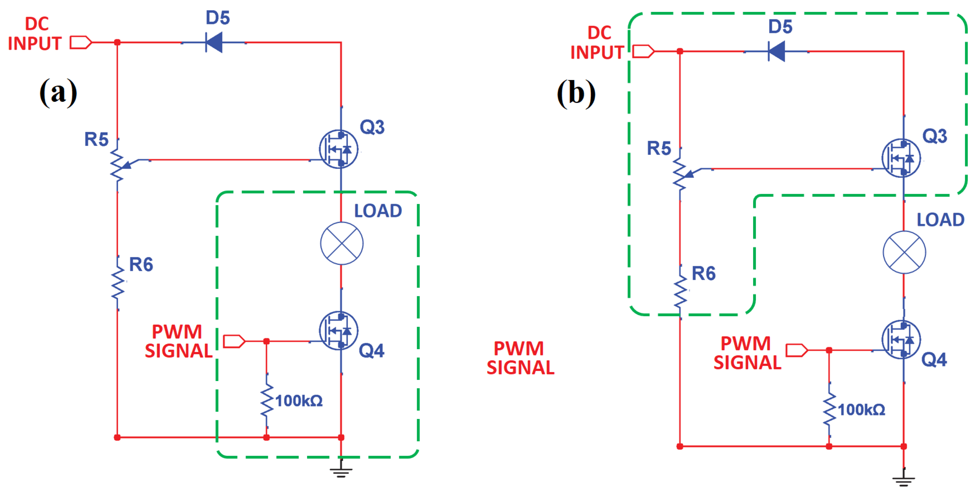
2.1.3. High-Power Drive Circuit Devices

MOSFET Gate Drive Circuit

Various drive circuit devices can be controlled with an electronic switching device, such as a MOSFET, and its “on state” and “off state” are controlled by a gate-to-source voltage signal. An N-channel MOSFET can be used to turn a high-current load on and off (such as a lamp, motor, etc.) using a low-voltage, low-current control signal of a PWM generator as shown in Figure 4a [32]. The PWM generator used in this prototype of the power supply is a PWM 753 as seen in Figure 5. MOSFETs’ gate-to-source voltage changes according to their application and power rating. Typically, a power MOSFET needs to be fully turned on at a voltage level between 10 and 20 V [33]. In this design, the low-voltage control signal from the PWM is connected to the gate of the transistor Q4 with 5 V from the Arduino nano. According to the control signal, the MOSFET switches the high voltage load on, and off. The load is connected between the source of transistor Q3 and the source of transistor Q4. The transistor Q4 has a resistor R7 to prevent static charge from building between the gate junction and ground (drain) of an n-channel MOSFET, because it can absorb energy in the device capacitances [34].

Dimmer Circuit

As seen in Figure 4b, the dimmer circuit is a drive circuit voltage controller built around a MOSFET in a source-follower design. The potentiometer R5 in series with a fixed resistor R6 connected across the power supply applies a variable positive gate-source voltage that turns on the MOSFET Q3. Consequently, when the voltage across the potentiometer wiper rises, the gate voltage rises as well. Eventually, this exceeds the MOSFET’s threshold voltage, turning on the device and transferring the voltage to the load. Because of the FET’s high input impedance, a potentiometer with a value of 100 kΩ or greater can be used, as its value is not crucial.

2.2. Software

Source Code in Arduino Sketch
The “setup ()” and “loop ()” functions make up the fundamental building blocks of the Arduino sketch. At the start of the programme, the setup function executes once. It is used to set up pins, declare constants, and declare variables. The loop function will run sequentially step by step. The loop function will automatically restart at the beginning when it reaches its end and continue to run. This runs continuously until the program is stopped. For programming, an Arduino Nano board and a model SH1106 display (Waveshare, TOP1 manufacturer) were used as seen in Figure 5. The source code for pulse time-on, frequency and duty cycle measurements are written below.
  • #include <SPI.h>
    #include <Wire.h>
    #include <Adafruit_GFX.h>
    #include <Adafruit_SH1106.h>
    #define OLED_RESET 4
    Adafruit_SH1106 display (OLED_RESET);
    #define pulse_ip 8
    float duty, freq, ontime, offtime, period;
    void setup ()
    {
    display.clearDisplay();
    pinMode(ledPIN, OUTPUT);
    pinMode(pulse_ip, INPUT);
    pinMode(hall_pin, INPUT);
    display.begin(SH1106_SWITCHCAPVCC, 0x3C);
    display.display();
    delay (3000);
    }
    void loop ()
    {
    display.clearDisplay();
    display.setTextSize(1);
    display.setCursor(0,21);
    display.setTextColor(WHITE);
    display.println(“FREQ(Hz):”);
    display.setTextSize(1);
    display.setCursor(0,38);
    display.setTextColor(WHITE);
    display.println(“DUTY (%):”);
    display.setTextSize(1);
    display.setCursor(0,55);
    display.setTextColor(WHITE);
    display.println(“T ON(ms):”);
    ontime = pulseIn (8, HIGH);
    offtime = pulseIn (8, LOW);
    period = ontime + offtime;
    freq = 1000000.0/period;
    duty = (ontime/period) * 100;
    display.setTextSize(2);
    display.setTextColor(WHITE);
    display.setCursor(56,17);
    display.println(freq);
    display.setTextSize(2);
    display.setTextColor(WHITE);
    display.setCursor(56,34);
    display.println(duty);
    display.setTextSize(2);
    display.setTextColor(WHITE);
    display.setCursor(56,51);
    display.println(ontime/1000);
    display.display();
    }

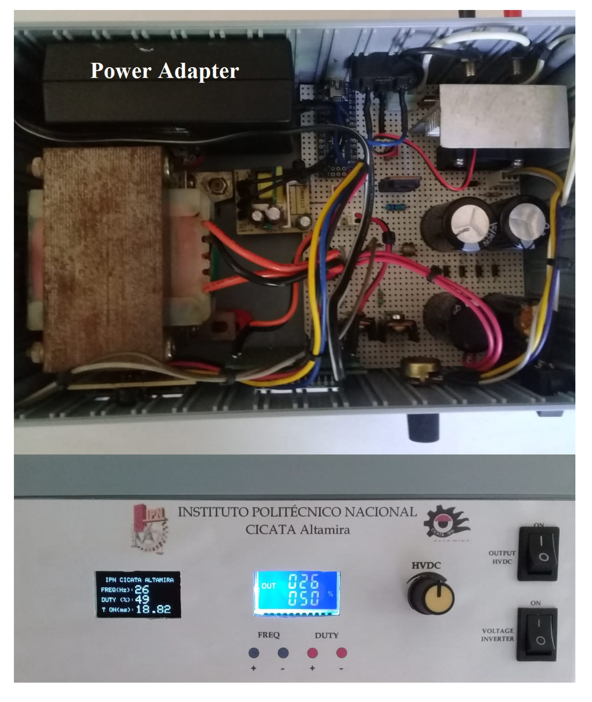
2.3. Pulsed HVDC Power Supply Circuit

For the construction of a pulsed HVDC power supply circuit, the following electronic scheme was designed, as shown in Figure 5 showing all the components used in this prototype. The circuit was designed and simulated using electronic software (Proteus 8.6, England). The prototype was mounted in a plastic casing to avoid an electric shock. As previously described, this circuit consists of a DC/AC inverter that increases from 12 VDC to 108 VAC, a voltage quadruple circuit to convert from 108 VAC to 430 VDC, a PWM generator to control the load and a circuit to adjust the output voltage. This circuit also has two protection fuses, one at the output of the transformer (108 VAC) and another connected to the source of the power transistor Q3 responsible for adjusting the output voltage. For further security and isolation, a switch was placed on the 12 VDC power supply to prevent the transformer from working all the time and another at the high voltage output to avoid electrical shocks with the terminals in case the capacitors are still charged. The frequency and duty cycle of the load are controlled by the 753 PWM generator (No/Brand), as shown in Figure 6c.

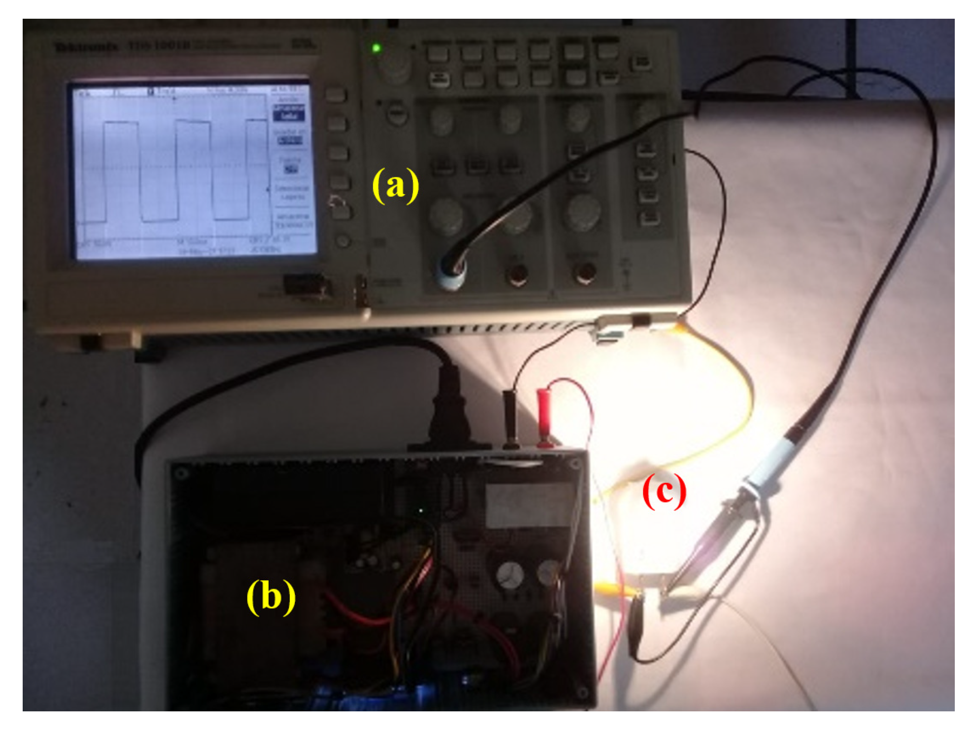
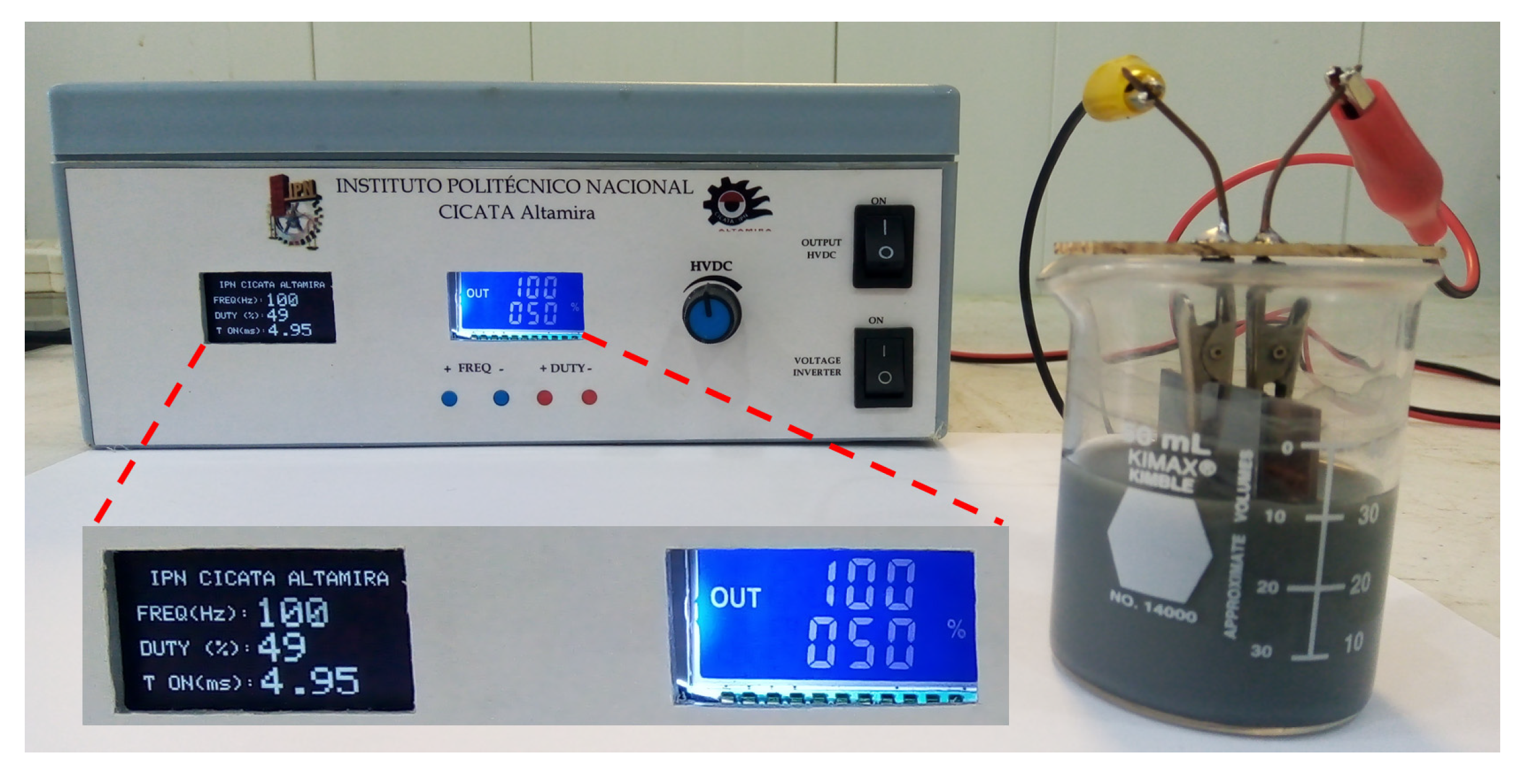
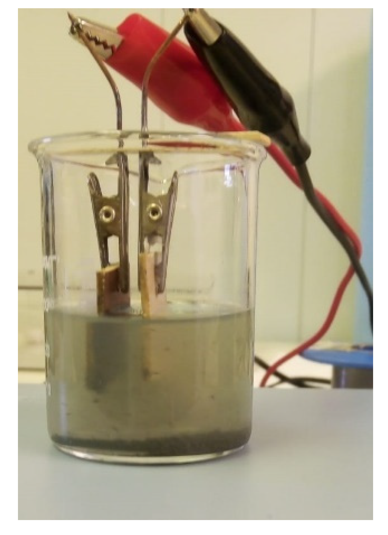
2.4. Experimental Setup

The output voltage was tested with the experimental setup shown in Figure 7. The prototype power supply performs HVDC switching according to the input pulse signal of the PWM generator, and the output voltage is stable by adjusting the potentiometer. The lamp used as a load was 5 watts, and the voltage was varied to turn it on and check that it turns on and off according to the PWM switching frequency. The switching frequency of the HVDC prototype was investigated by monitoring the voltage waveform using the Tektronix TDS 1001B oscilloscope. The duty cycle was kept constant at 50%, while the output voltage and frequency were varied.

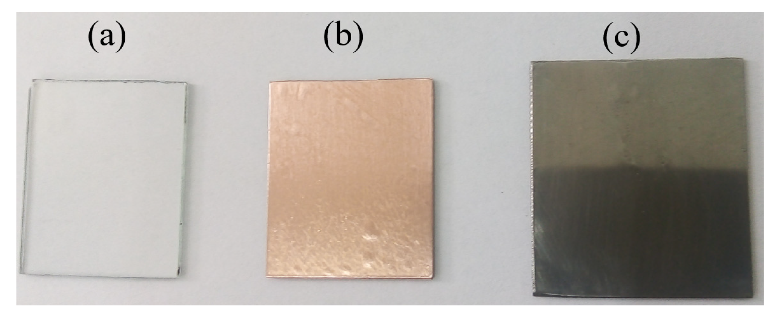
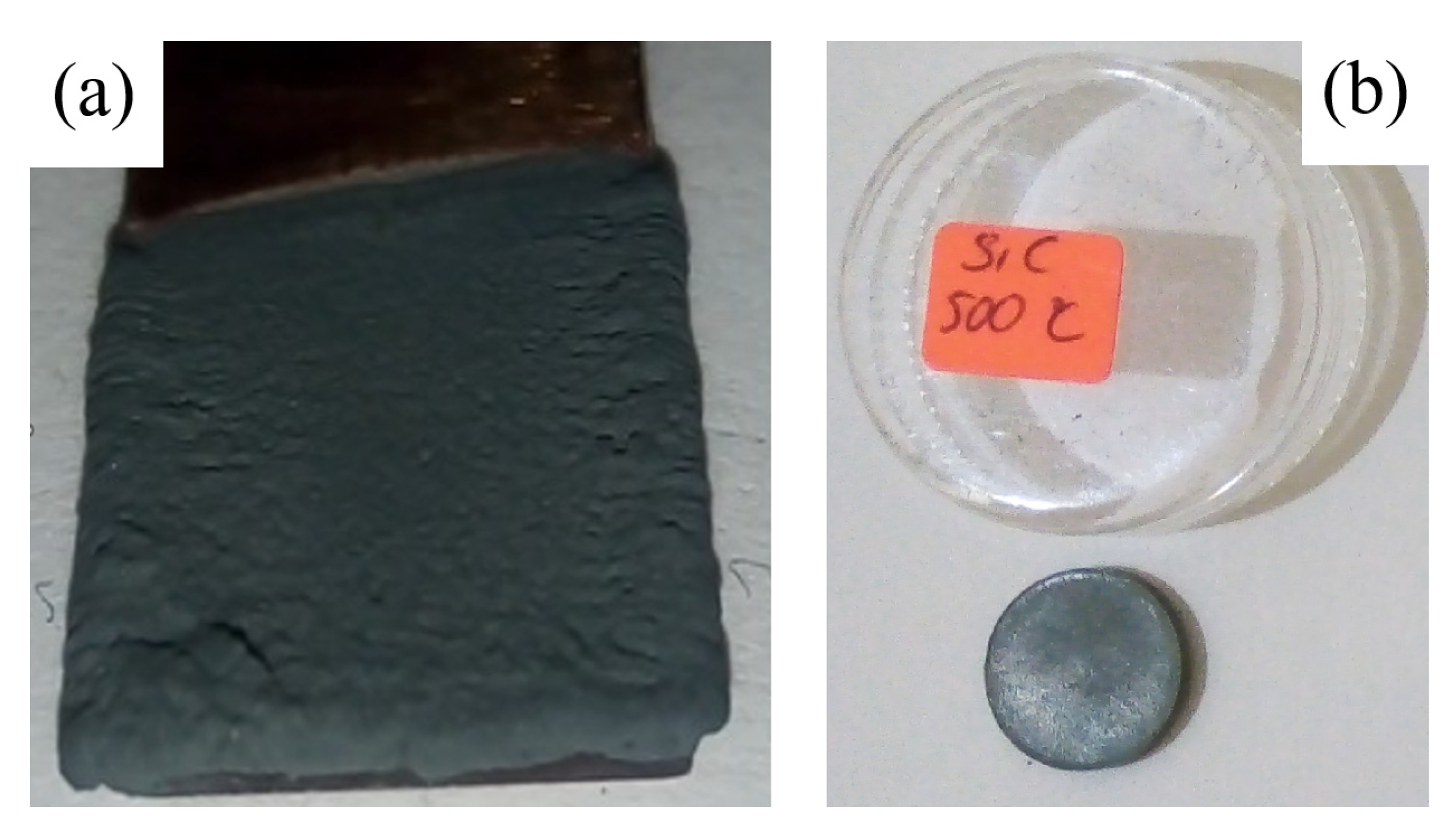
2.5. Experimental Details of SiC Coatings

Commercial β-SiC powder (Sigma Aldrich, Shanghai, China) with a particle size < 100 nm, polyvinylbutyral (PVB, Sigma Aldrich, Taiwan) as a binder and acetone (Fermont, Mexico City, Mexico) as a solvent were used. Commercial η-Al2O3 powders (Sigma Aldrich, Hamburg, Germany) with a particle size < 50 nm and commercial graphite powders (Sigma Aldrich, St. Louis, MO, USA) with a particle size < 20 µm were used as additives. The concentration of the suspension was 10 g/L of SiC and 5 g/L of PVB in 30 mL of acetone. The suspensions were prepared of only SiC and mixtures of SiC and alumina (SiC-Al), SiC and graphite (SiC-C) and SiC mixtures with graphite + aluminium (SiC C-Al), using different concentrations of alumina and graphite. Table 1 shows the nomenclature and compositions of the deposited samples at room temperature (RT). The EDP was carried out on 304 stainless steel as a cathode of 30 × 50 mm in size with an electrical conductivity of 2 × 10⁶ S/cm [35] and copper tape as an anode with an electrical conductivity of 6 × 10⁷ S/cm [35] on a glass substrate of 25 × 30 mm in size to avoid deposition on both sides of the copper electrode, as shown in Figure 8.
EDP pulsed with the square-shaped symmetric waveform, a potential difference of 100 VDC pulsed, frequency of 100 Hz, 50% cycle duty and 7 mm distance between electrodes, and the suspension was then deagglomerated using a high-energy ultrasonic bath for 5 minutes. Figure 9 shows the experimental setup for the preparation of SiC samples.
After being deposited (Figure 10a), the material was taken off the copper substrate and compacted under a pressure of 5 tons into 12.7 mm-diameter disc-shaped pellets for 5 minutes and then subjected to heat treatment at atmospheric pressure for 3 h at 500 °C (Figure 10b) in order to eliminate the remains of organic material used during the deposition process (PVB) and then carry out the characterizations. Due to the necessity of to carry out these procedures after the coatings, a study on the power supply, electrodes and solute–substrate interaction was omitted in favour of another research work.
The crystalline structure of bulk samples was determined via X-ray diffraction (XRD) using a D8 Advance diffractometer with Cu-Kα radiation, 20° to 80° in 2θ with a step size of 0.02 and a scan speed of 1 s, and to identify the crystalline phases the ICSD (Inorganic Crystal Structure Database) references were used, Raman spectra on a LabRam HR 800 Raman spectrometer, scanning electron microscopy (SEM) was used for morphology and chemical analysis was performed using energy-dispersive X-ray spectroscopy (EDXS) on a FEI brand Quanta FEG 250. The electrical conductivity and Seebeck coefficient were measured simultaneously with a Netzsch SBA 458 Nemesis in the range from 100 to 500 °C with a heating rate of 5 K/min, under a continuous nitrogen flow of 10 mL/min, and a DC current of 50 mA was applied. Thermal conductivity was calculated by using Equation (3), given below:
κ = λ ρ c p
where κ is the total thermal conductivity (W/m·K), λ is the thermal diffusivity, cp is the specific heat and ρ is the density sample. Thermal diffusivity values were measured with a Netzsch LFA 467 Hyperflash from 100 to 500 °C with a heating rate of 20 K/min, under a continuous nitrogen flow of 10 mL/min, and density and cp values were obtained from the literature [36]. Thermoelectrical properties were determined up to 500 °C due to the operating range of the infrared detector of the LFA 467, which is RT to 500 °C. Electronic and lattice contributions to the thermal conductivity were calculated based on the Wiedemann–Franz law using Equations (4) and (5) given below:
κ = κ E + κ L
and
κ E = L σ T
where κ is the total thermal conductivity (W/m·K), κE is the electronic contribution to the thermal conductivity (W/m·K), κL is the lattice contribution to the thermal conductivity (W/m·K), L is the Lorentz number (2.45 × 10⁻⁸ V2/K2 for degenerate semiconductors), σ is the electrical conductivity (S/m) and T is the absolute temperature (Kelvin, K) [37].

3. Results

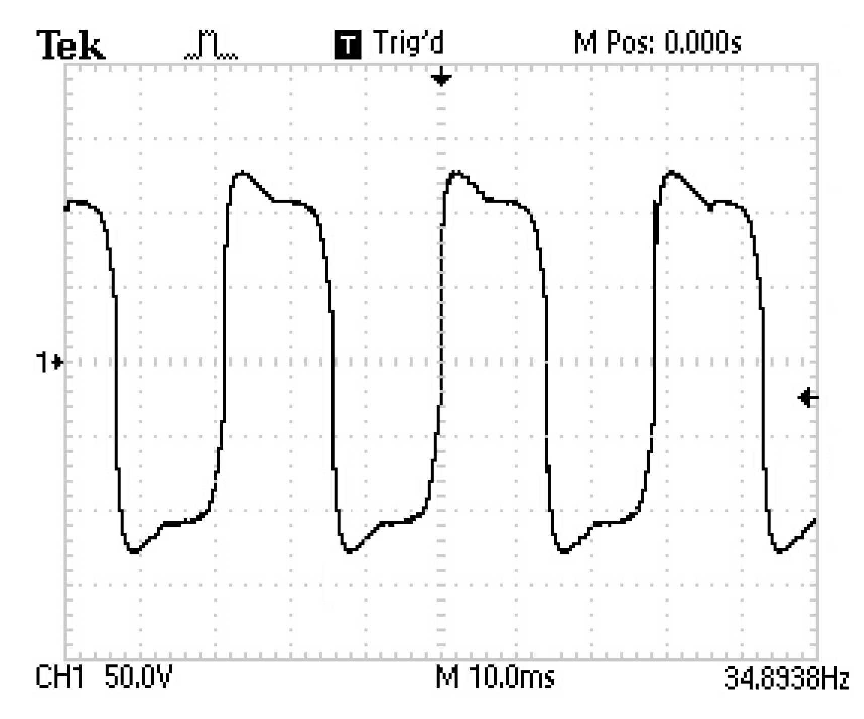
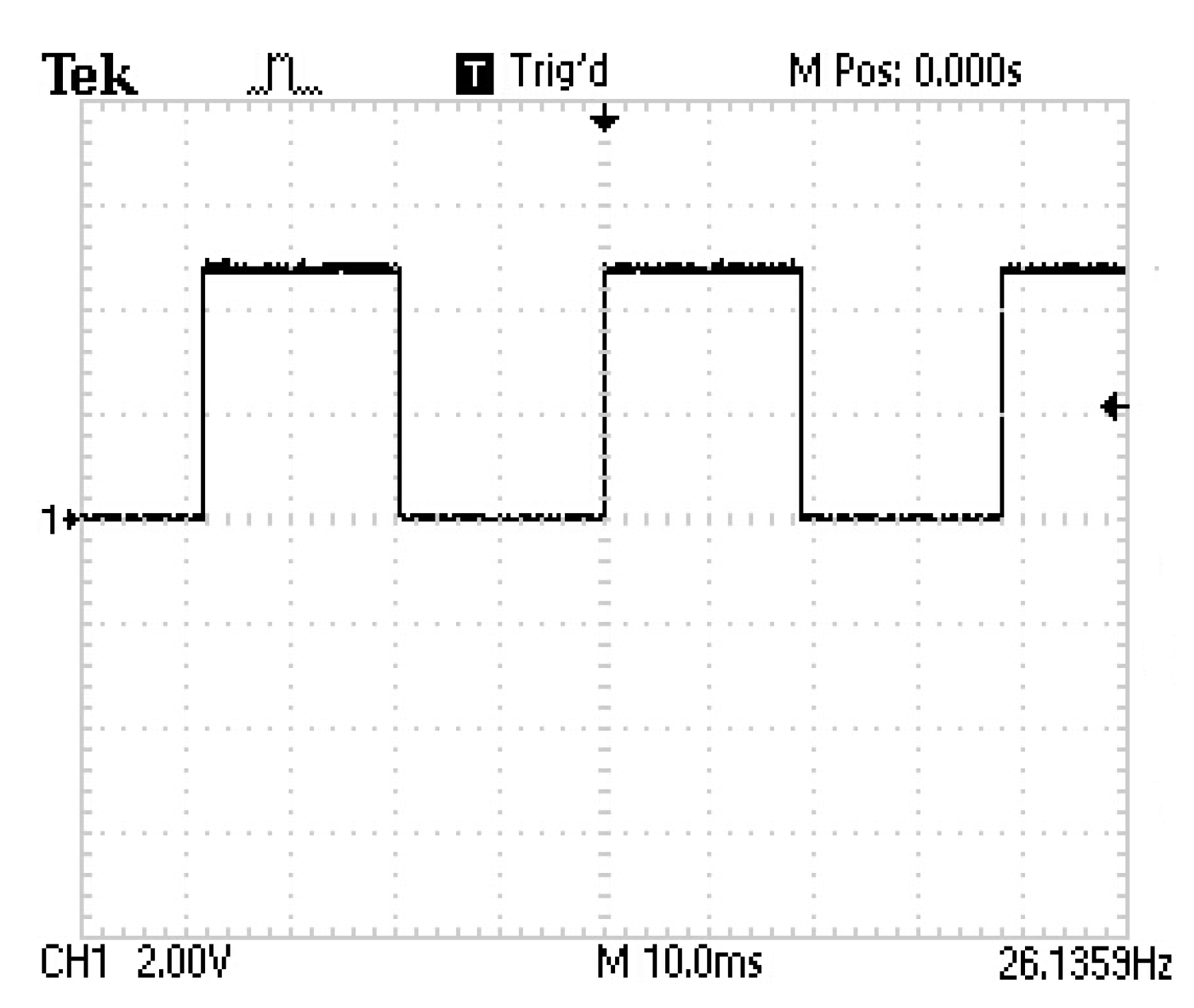
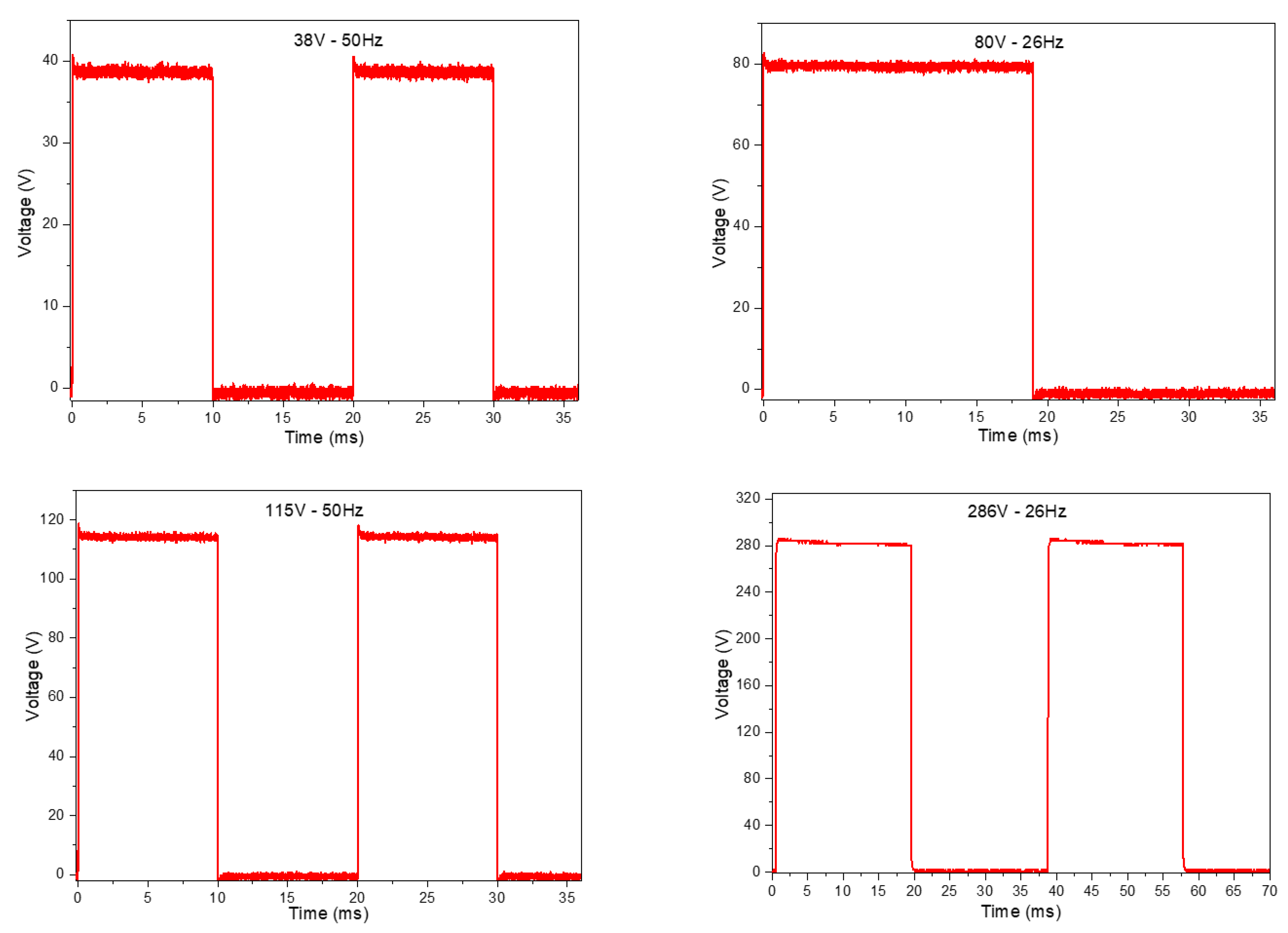
3.1. Results of the Pulsed HVDC Prototype

The specifications of the pulsed HVDC prototype are shown in Table 2. The input current was limited by the power adapter used in the prototype, as seen in Figure 11.
Both the frequency and the period of the output of the voltage inverter in the transformer (T) were measured with the oscilloscope, and the waveform is depicted in Figure 12. It was observed that the measured RMS (Root Mean Square) voltage is 108 V, with a quasi-sinusoidal wave that oscillates between the positive pole and the negative pole in a period of 28.65 ms and frequency of 34.89 Hz.
Subsequently, the signal at the output of the PWM generator was measured to observe that there are no variations in the frequency and duty cycle. To make the measurements, a frequency of 26.13 Hz and 50% duty cycle were chosen, as shown in Figure 13. The voltage of 4.8 V corresponds to the voltage supplied to the Arduino Nano board.
Finally, measurements were made at 26 Hz and 50 Hz with a 50% duty cycle, without load and varying the output voltage to observe the switching states of the MOSFET Q4. Figure 14 shows the waveforms without load obtained from the different switching states at different voltages. It can be noticed that the voltage signals are square waves, and when the time is HIGH, they show negligible distortion.

3.2. Results and Discussions of Bulk SiC Samples

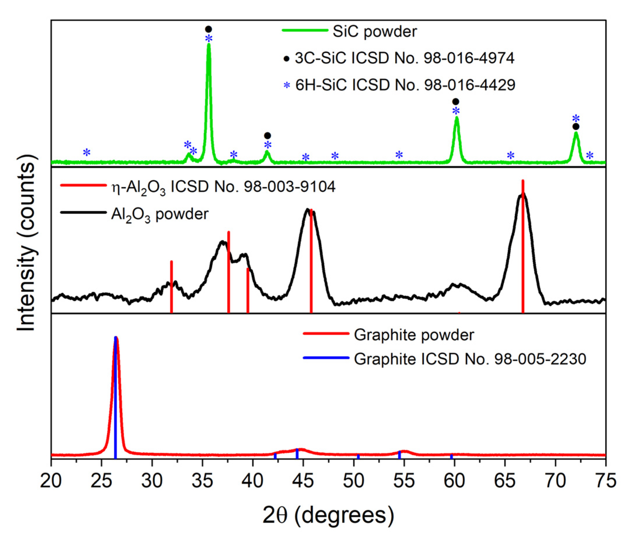
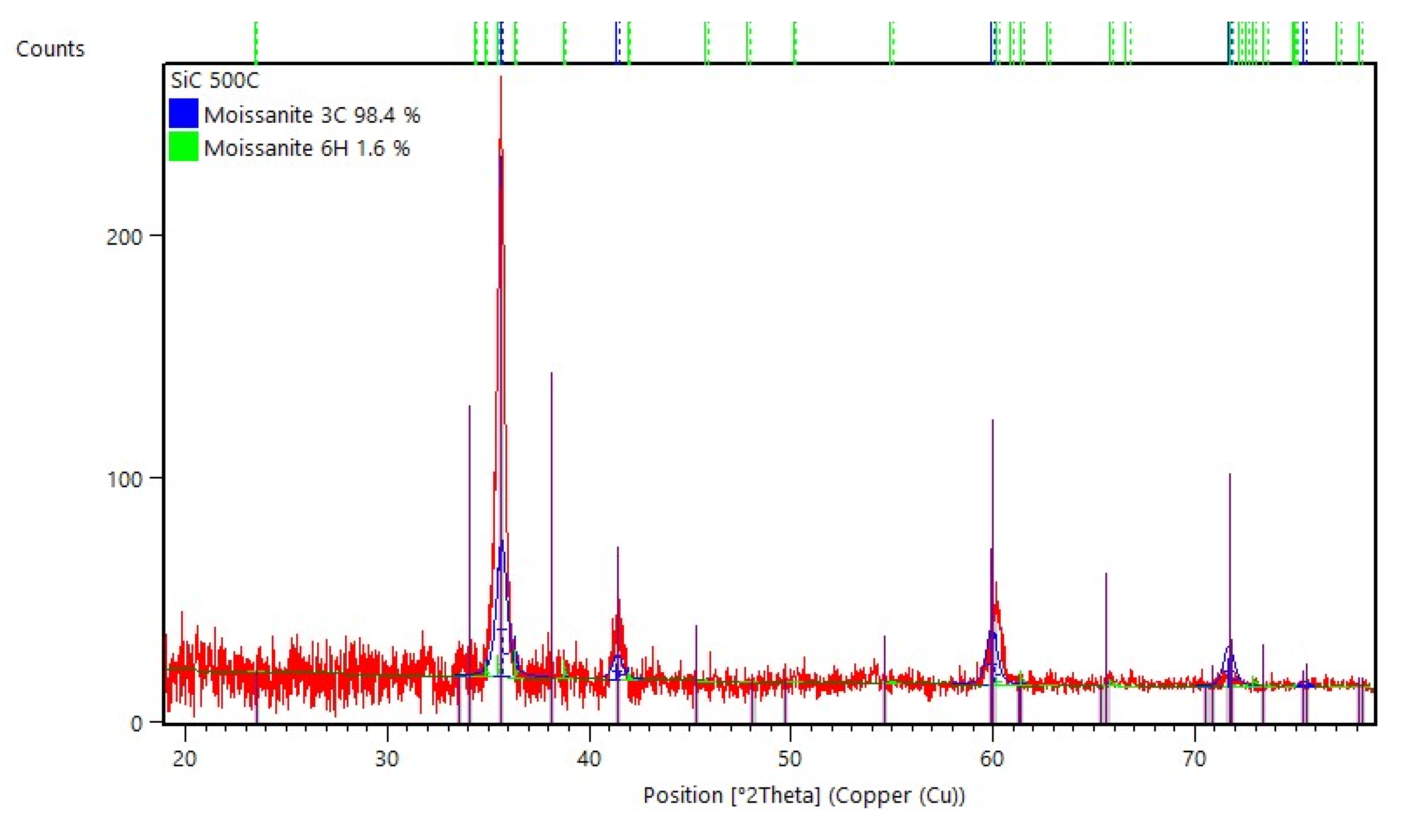
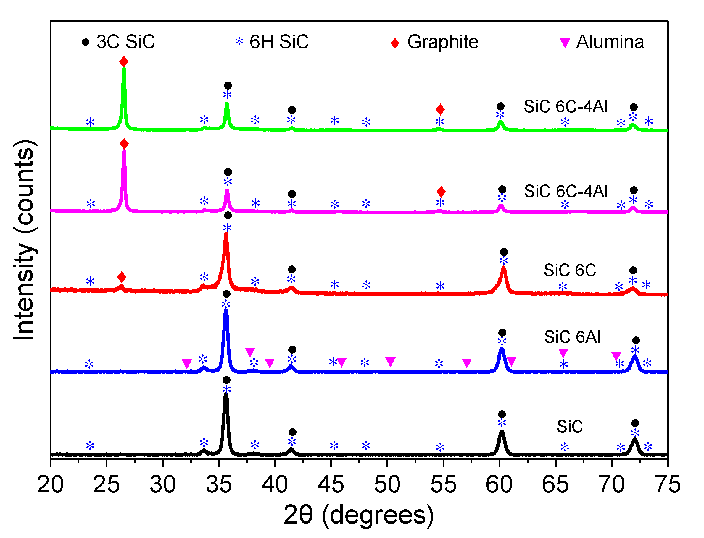
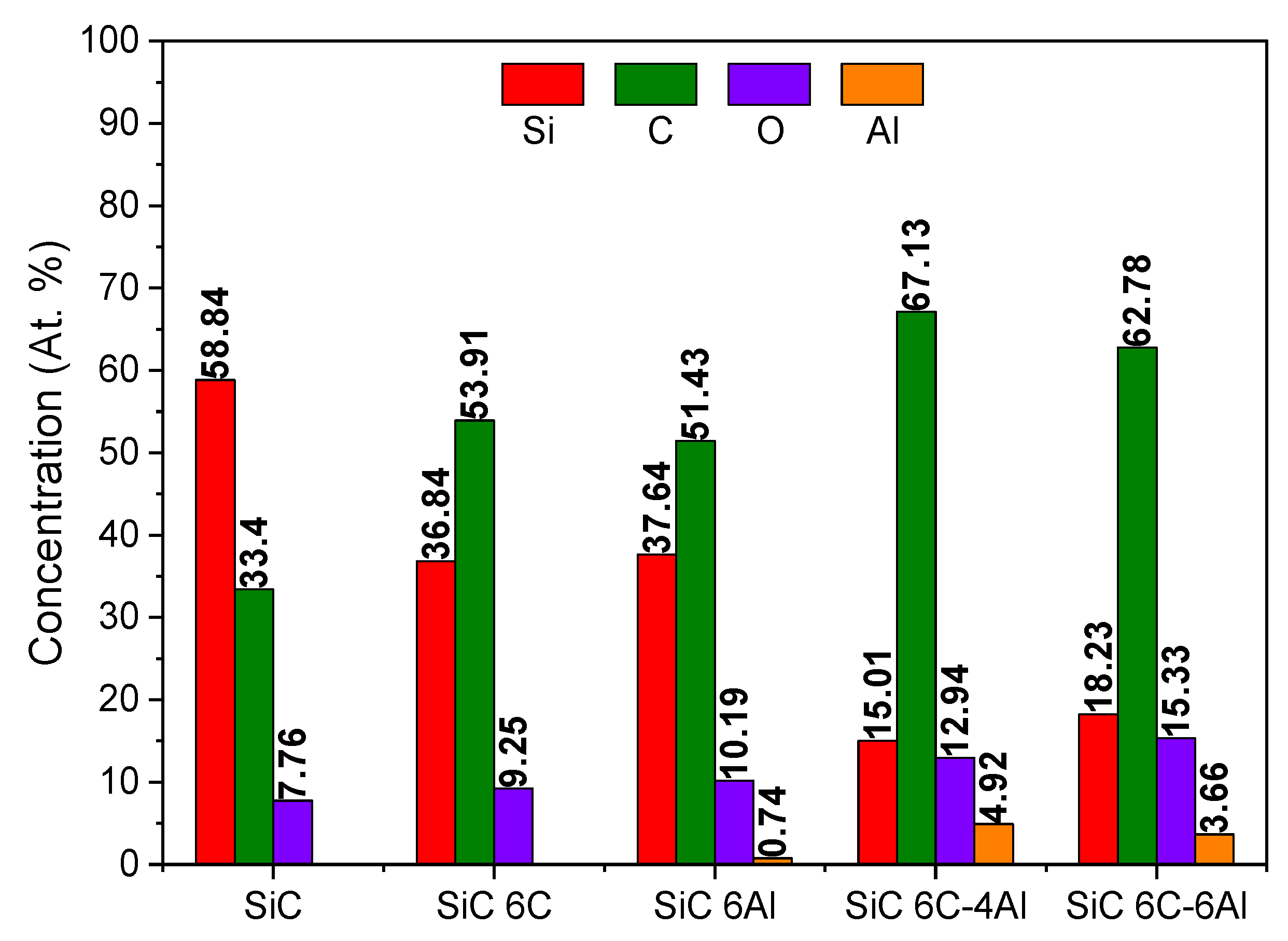
3.2.1. Structural Analysis

The X-ray diffraction patterns of SiC, alumina and graphite powders are shown in Figure 15. The SiC powder exhibits only major peaks corresponding to the 3C polytypes of an FCC cubic phase (ICSD 98-016-4974) and in lower-intensity peaks related to the 6H polytype at the angles 2θ = 33.63° and 38.11° (ICSD 98-016-4429). Due to the overlap between the Bragg reflections of the SiC polytypes, the Rietveld method was used to determine the weight percentage of the different phases present in the SiC and the PANalytical Highscore Plus 3.0 (Malvernpanalytical) software was used. The refined experimental data for SiC are seen in Figure 16 where the coloured symbols indicate the weight percentage of each phase. The quality of the refinement can be verified based on the good correspondence between the simulated and experimental pattern and by the values of the main refinement parameters, as shown in Table 3.
For the alumina powder, the pattern shows signals related to the η-Al2O3 with cubic structure FCC (ICSD 98-003-9104). In the case of graphite powder, the XRD pattern shows planes to a 2H hexagonal structure (ICSD 98-005-2230). Figure 17 shows the XRD patterns of the samples of SiC and SiC-Al and/or SiC-C. The diffractogram of the SiC-6C sample exhibits a small peak at an angle of 2θ = 26.27°, which corresponds to the crystallographic plane (002), but in the samples mixed with alumina, the presence of the additive and the characteristic peaks is not observed. Otherwise, the SiC Al+C samples present a higher intensity at the angle 2θ = 26.27° and a small peak at 2θ = 54.63° corresponding to graphite and a decrease in the intensity of SiC; furthermore, no peaks related to the alumina added to SiC are observed.

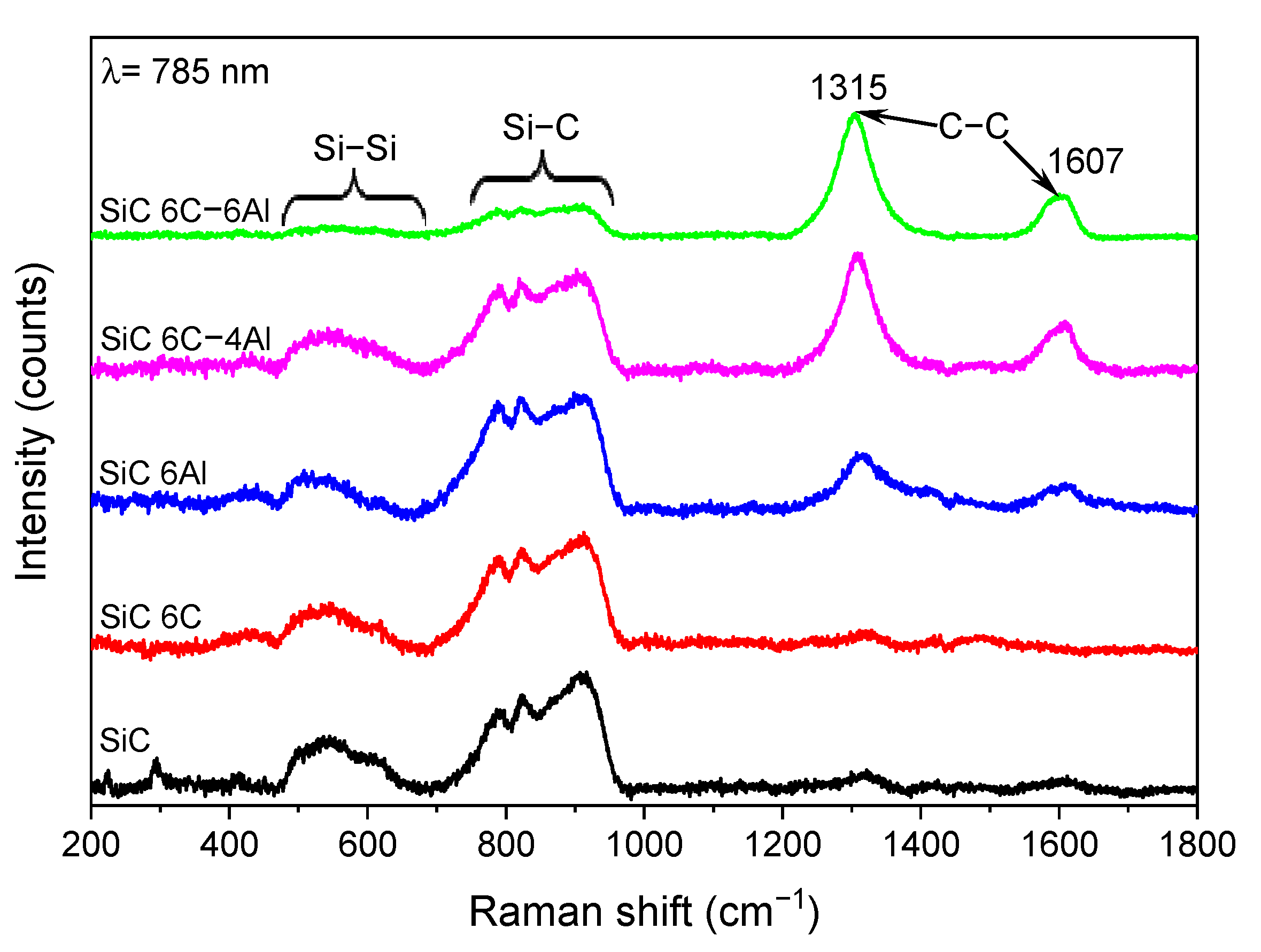
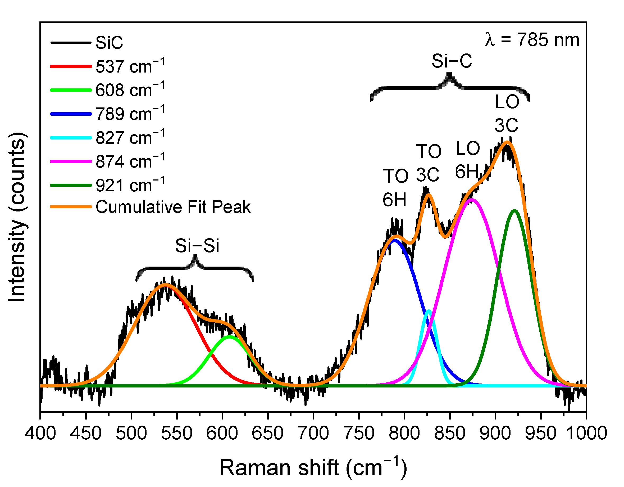
3.2.2. Raman Spectroscopy Analysis

Raman spectroscopy of SiC was carried out to analyse the structural properties of the samples. Figure 18 shows the Raman spectra of the samples calcined at 500 °C and presents three different bands in the regions of 450–700 cm−1, 700–1000 cm−1 and 1200–1700 cm−1. The 450–700 cm−1 band is attributed to the activation of Raman modes related to silicon acoustic phonons.
The peak at 608 cm−1 of the deconvoluted Raman spectrum in Figure 19 belongs to the Si-Si bond, this peak at higher wavenumber values and corresponds to a compression stress in these bonds; that is, they are shorter than they should be in unstressed Si−Si tetrahedra, which is the signal at 537 cm−1. SiC exhibits modes around 789 cm −1 and 874 cm−1 corresponding to the transverse (TO) and longitudinal (LO) optical Raman for 6H-SiC, respectively. Furthermore, modes at 827 cm−1 and 921 cm−1 were identified as the transverse and longitudinal optical phonons of 3C-SiC, respectively (Figure 19). The wide bands between 700 and 1000 cm−1 indicate the presence of high structural disorder in SiC bonds and are therefore attributed to the optical Raman modes of 6H-SiC [38]. The 1607 cm−1 signal is related to C−C vibrations in amorphous carbon [39]. Finally, the 1353 cm−1 signal is similar to the transverse optical Raman (TO) signal of diamond, indicating the presence of C−C sp3 bonds in 3C-SiC [40].
Figure 18 also shows the Raman spectra of SiC, SiC-Al and/or SiC-C. It is observed that when alumina is added to SiC, there is an increase in the intensity of the signals at 1315 cm−1 and 1607 cm−1. Therefore, the changes in the Raman spectra are caused by the addition of Al2O3. The increase in the concentration of C + Al2O3 causes a decrease in the intensity of the band in the range of 700–1000 cm−1. In addition, it is observed that the intensities of the signals at 1315 cm−1 increase with the increase in the Al2O3 content, indicating the addition of this compound [41].

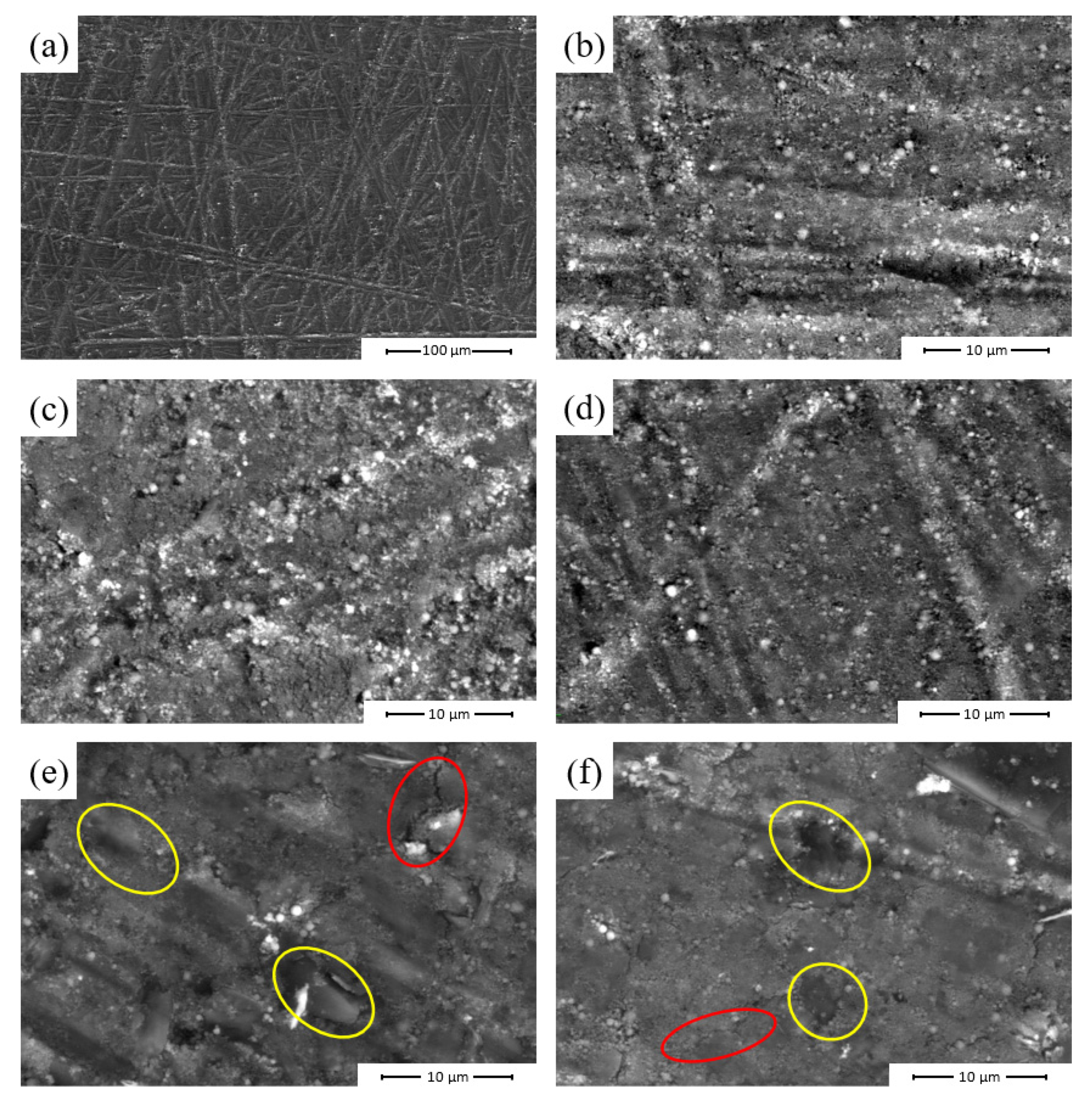
3.2.3. Scanning Electron Microscopy Analysis

Figure 20 depicts SEM micrographs of samples compacted and heat-treated at 500 °C for 3 h. Figure 20a shows a fluted caused by the plunger after compaction, and the same phenomenon was observed in all the samples. In the compacted samples (Figure 20a–e), porosity and fractures are observed, possibly due to the low treatment temperature. On the other hand, in Figure 20e,f graphite crystals with particle sizes smaller than <10 μm can be observed.
During the manufacturing process, it was observed that a small portion of the material in the suspension precipitated (Figure 21), and consequently, an elemental analysis via EDXS was performed to investigate the conservation of the stoichiometry proposed in the methodology for the coatings. Figure 22 shows the results obtained. This analysis indicated the presence of Si, C, O and Al atoms as the main chemical components present in the samples. The experimentally obtained composition of the elements Si, C, O and Al did not coincide with the values initially proposed, which indicates that the electrophoretic method does not maintain the relationship of the theoretical composition with the experimental composition, possibly due to the difference in the particle size of the additives and their interaction with the applied electric field.

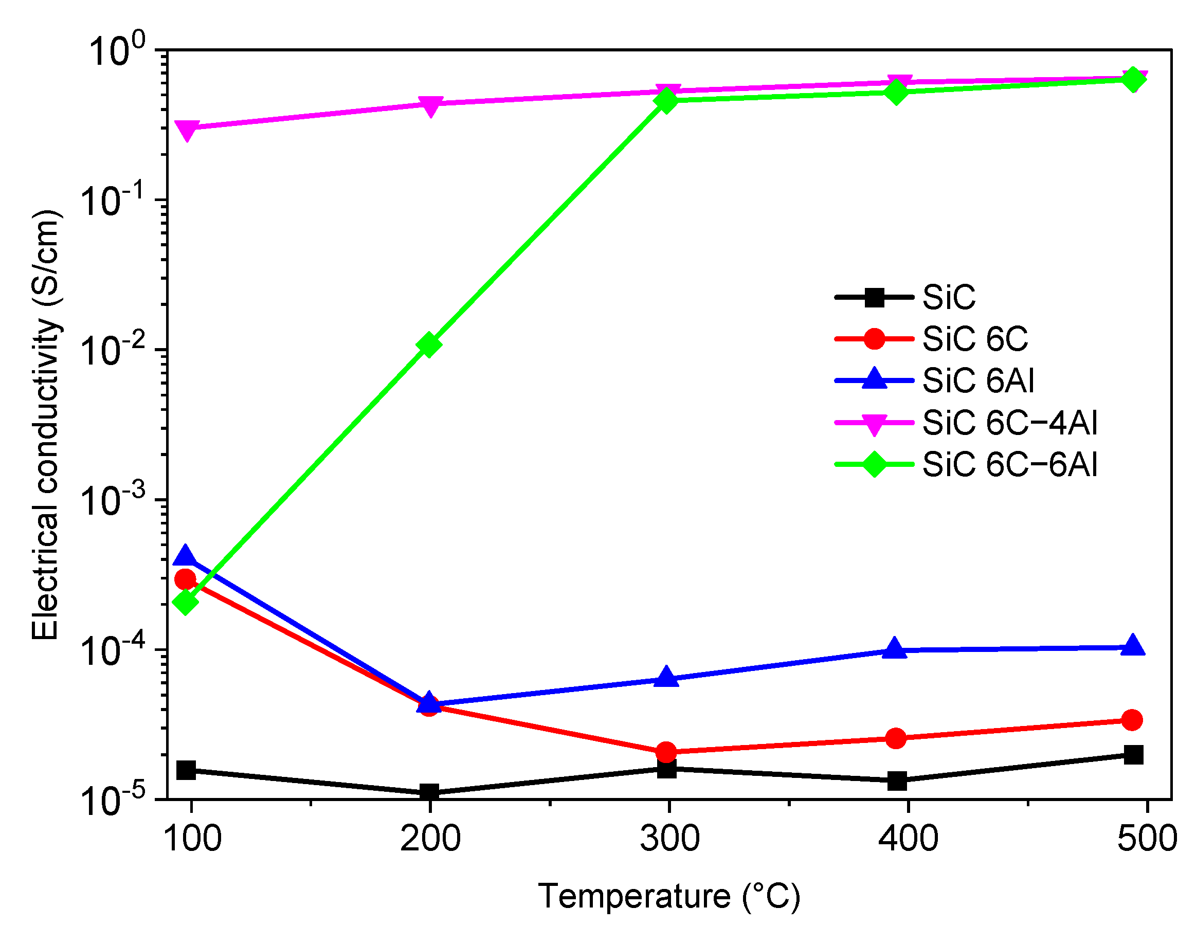
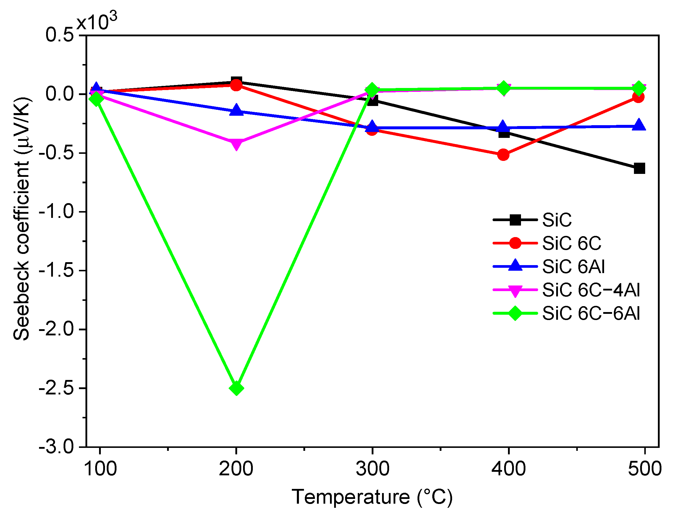
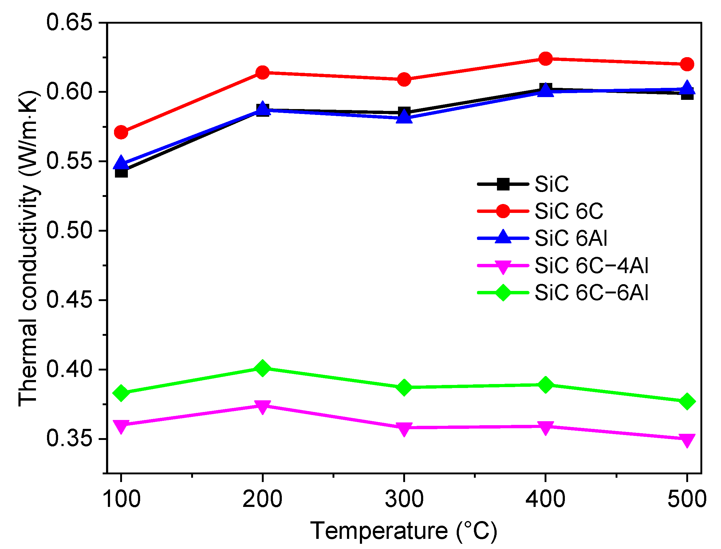
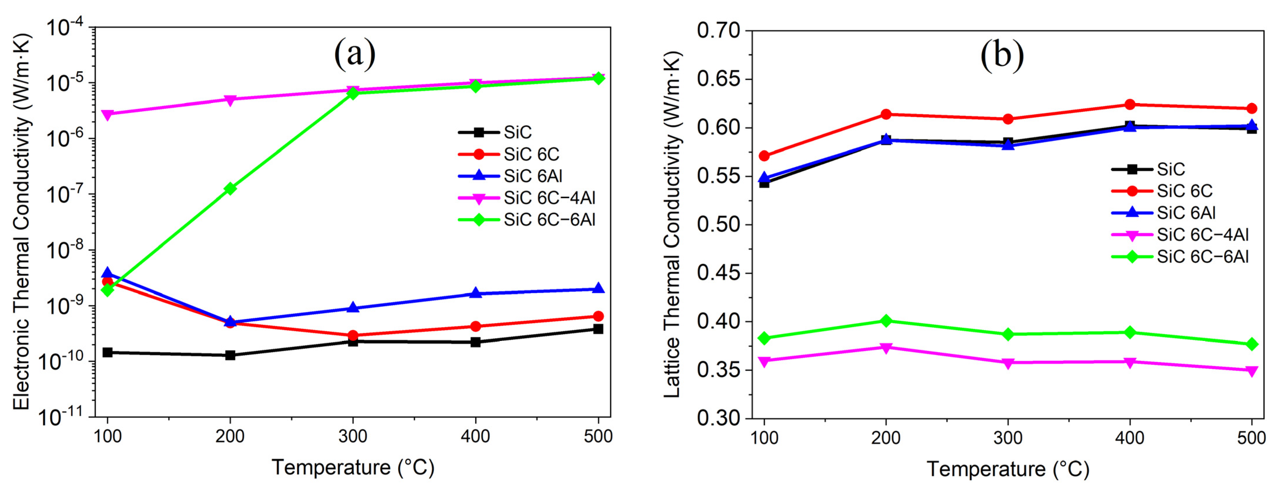
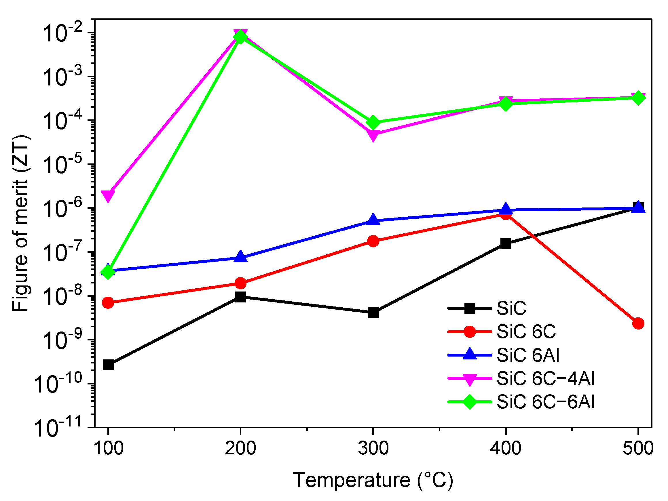
3.2.4. Thermoelectric Properties

Figure 23 shows the electrical conductivity (σ) as a function of the measured temperature of the SiC samples mixed with alumina and/or graphite and for the SiC sample heat treated at 500 °C. As seen in Figure 23, electrical conductivity of the SiC sample does not show a significant change. The SiC-6C sample decreases the electrical conductivity showing a metallic behaviour [42] from 100° to 300 °C and then increases the electrical conductivity from 300 to 500 °C showing a semiconductor behaviour [43], and a similar case occurs with the SiC 6Al sample, whereas the σ of the SiC 6C-4Al sample increases monotonically with an increasing temperature until reaching 500 °C and achieving σ = 0.65 S/cm. On the other hand, the SiC 6C-6Al sample shows a semiconducting behaviour from 100 to 300 °C obtaining a σ = 0.45 S/cm to then grows monotonically from 300 to 500 °C showing a metallic behaviour in that temperature range. For the samples without additive and mixed only with alumina or graphite, the electrical conductivity is low with respect to the samples added with C + Al2O3, which show a result of four orders of magnitude higher than the aforementioned samples in the range of 300 to 500 °C. The slight increase in electrical conductivity in the SiC 6C-4Al and SiC 6C-6Al samples may be due to the help in the sintering process provided by the alumina during heat treatment and to the conductive property of graphite.
Figure 24 shows the Seebeck coefficient (S) as a function of temperature for the samples of SiC mixed with alumina and/or graphite and for the sample additive-free. The samples showed an n-type semiconductor behaviour. The Seebeck coefficients of the samples showed distributed values in all the temperature ranges; for example, the Seebeck coefficient of the SiC additive-free increased with an increasing temperature, obtaining values of 15 to −630 μV/K. This maximum value is equal to or greater than that reported by Masuda et al. in the temperature range of 400~500 °C with a Seebeck coefficient ≈ −600 μV/K [44]. The highest Seebeck coefficient was measured for the SiC 6C-4Al sample and was observed at 200 °C to be roughly −2500 μV/K due to a strain-induced redistribution of the effect states caused by interface mismatch, as informed by Cramer et al. [45], obtaining high Seebeck coefficients for their Si/SiC multilayer thin-film systems and reported values of −2600 μV/K at 870 K.
Figure 25 shows that the thermal conductivity (κ)of the SiC, SiC 6C and SiC 6Al samples tended to increase with an increasing temperature due to the metallic behaviour of the material [42], while in the SiC 6C-4Al and SiC 6C-6Al samples, the thermal conductivity tended to decrease with an increasing temperature due to Umklapp phonon dispersion [46], obtaining values of 0.35 W/m·K and 0.377 W/m·K at 500 °C, respectively.
These results are lower than previously reported [14]. The thermal conductivity was reduced by an average of 35% to 43% with respect to the SiC, SiC 6C and SiC 6Al samples. It was observed that the reduction rate of thermal conductivity is greater at high temperatures for the samples added with C + Al2O3; the effect of porosities may explain this outcome, in addition to the Umklapp processes, as mentioned above [47,48]. Furthermore, the addition of graphite could contribute to reducing the thermal conductivity [24,49] due to the thermal resistance of the interface generated by the excess graphite [50]. As stated above, increasing σ and reducing κ of SiC are crucial to improve its TE performance. In this sense, the addition of graphite could also increase the electrical conductivity [24], and the addition of alumina could help to reduce the thermal conductivity [25] to increase the thermoelectric efficiency.
Figure 26 show the temperature-dependent electronic and lattice contributions to the thermal conductivity of the SiC and SiC added with alumina and/or graphite samples. It was observed that the electronic κE increases slightly due to the metallic nature of the material [42]. The κL also decreases despite the slight increase in κE of the SiC 6C-4Al and SiC 6C-6Al samples, which decreases the total thermal conductivity of the samples.
The ZT values of SiC samples mixed with graphite and/or alumina are shown in Figure 27, and the highest ZT results of different studies on the thermoelectric properties of SiC can be found in the literature. Okamoto et al. sintered SiC with 0.5–60 wt.% B4C under an Argon atmosphere reaching a maximum ZT value of 5 × 10⁻⁶ at 873 K with a B4C concentration of 20 wt.% [51]. Qiao et al. studied the TE properties of SiC reaction-bonded SiC with free-Si. The maximum ZT value was 4.2 × 10⁻⁴ at 723 K and was obtained with a free Si content of 20.43 wt.% [52]. Ivanova et al. produced polycrystalline 3C-SiC codoped with nitrogen and boron. The power factor was improved, but due to the high thermal conductivities of the samples, low ZT values were obtained with a maximum value of 0.018 × 10⁻³ at 1100 K [53]. Koumoto et al. produced porous SiC ceramics with ≈ 60% relative density through the hot pressing of α and β-SiC in nitrogen and argon atmospheres. A maximum ZT of approximately 3 × 10⁻⁵ was achieved using the study’s combined method of decreasing heat conductivity based on porosities and increasing electrical conductivity with nitrogen doping [54]. Cagri et al. used a TiC segregated network structure approach to improve the thermoelectric properties of SiC, reporting a maximum ZT of 5.04 × 10⁻³ at 923 K, with the TiC content at 1.5 vol% [55]. In this study, the TE properties of SiC were improved over previously reported ZT values.
A maximum ZT value of ≈0.01 was obtained with an addition of 6 wt.% C and 4 wt.% Al2O3 at 200 °C, which corresponds to an increase of ≈ 200% with respect to that reported by Cagri et al. Although the ZT values achieved in this study were smaller than typical TE materials, such as BiTe-based alloys, and even high-temperature materials, such as HH and SiGe alloys, these materials generally decompose, melt or oxidize at temperatures above 1000 °C [54]. Since the ZT values of SiC with graphite and/or increase with an increasing temperature, this material appears to have high potential for high-temperature TE applications [56].

4. Conclusions

In conclusion, SiC and SiC samples mixed with graphite and/or alumina were deposited using the electrophoretic method, with a proprietary design of a power supply with a pulsed voltage of 100 VDC, and then pelletized with the deposited material and heat treated at 500 °C to obtain compact samples and achieve better thermoelectric performance. The high phonon dispersion and porosities of the SiC samples could contribute to the improved Seebeck coefficient and thermal conductivity, although the electrical conductivity was low. A maximum value of ZT ≈ 0.01 was obtained at 200 °C with a concentration of 6 wt.% C and 4 wt.% Al2O3. These results demonstrate that an optimal concentration of additives for SiC could improve the TE properties of the material. These findings provide useful information for researchers seeking to select a rapid, simple and low-resource-consuming method to obtain coatings of diverse materials for thermoelectric applications.

Author Contributions

Conceptualization, writing—original draft, methodology, investigation and editing, J.J.R.V.; project administration, supervision, analysis and writing—review and editing, E.R.G.; and project administration, supervision and writing—review and editing, E.C.D.l.C.T. All authors have read and agreed to the published version of the manuscript.

Funding

This work was funded by a science grant from the Consejo Nacional de Humanidades, Ciencias y Tecnologías (CONAHCYT) and SIP project 2021-0304, 2022-0655 and 2023-0826 through the Instituto Politécnico Nacional (IPN) and CONAHCYT project 1905.

Data Availability Statement

Data are contained within the article.

Acknowledgments

Instituto Politécnico Nacional and Centro de Investigación en Ciencia Aplicada y Tecnología Avanzada (CICATA) Unidad Altamira; Consejo Nacional de Humanidades, Ciencias y Tecnologías.

Conflicts of Interest

The authors declare no conflicts of interest.

References

  1. Jaiwanglok, A.; Eguchi, K.; Julsereewong, A.; Pannil, P. Alternative of high voltage multipliers utilizing Cockcroft–Walton multiplier blocks for 220 V and 50 Hz input. Energy Rep. 2020, 6, 909–913. [Google Scholar] [CrossRef]
  2. Kenfack, P.; Dandoussou, A.; Nkale, E.F. Comparative study of the design and simulation of an AC to high DC voltage generation circuit. J. Electr. Syst. Inf. Technol. 2022, 9, 1–17. [Google Scholar] [CrossRef]
  3. Berkhout, M. Integrated Audio Amplifiers in BCD Technology; Springer Science and Business Media LLC: New York, NY, USA, 1997; ISBN 9781461377870. [Google Scholar]
  4. Nakashima, D.; Kino, Y.; Eguchi, K. Design of a bipolar Dickson voltage multiplier suitable for low output voltage condi-tions to provide efficient food processing. Energy Rep. 2023, 9, 207–213. [Google Scholar] [CrossRef]
  5. Song, H. VLSI Modulation Circuits—Signal Processing, Data Conversion, and Power Management; Lulu Press: Morrisville, NC, USA, 2014. [Google Scholar]
  6. Gerber, D.L.; Liou, R.; Brown, R. Energy-saving opportunities of direct-DC loads in buildings. Appl. Energy 2019, 248, 274–287. [Google Scholar] [CrossRef]
  7. Singh, B.P.; Singh, R. Electronic Devices and Integrated Circuits; Dorling Kindersley: Noida, India, 2009. [Google Scholar]
  8. Thaker, U.; Vora, S.C.; Amardas, A.; Amal, S.; Saurabh, K.; Chakraborty, A.; Christian, P.; Mankani, A.; Baruah, U. Design, analysis, fabrication and testing of 100 kV, 100 mA DC full-wave voltage multiplier (FWVM) modular unit for accelerator power supply. Fusion Eng. Des. 2023, 192, 113612. [Google Scholar] [CrossRef]
  9. Sharma, A.K. Semiconductor Electronics; New Age International: New Delhi, India, 2008. [Google Scholar]
  10. Amrollahi, P.; Krasinski, J.S.; Vaidyanathan, R.; Tayebi, L.; Vashaee, D. Electrophoretic Deposition (EPD): Fundamentals and Applications from Nano- to Microscale Structures. In Handbook of Nanoelectrochemistry; Springer International Publishing: Berlin/Heidelberg, Germany, 2016. [Google Scholar]
  11. Li, C.; Li, Y.; Chen, Q.; Sun, D.; Li, H.; Chen, W.; Yan, J.; Wu, G.; Yuan, X.; Wang, S.; et al. Ti3C2Tx@polyaniline/epoxy coating based on cathodic electrophoretic deposition with effective corrosion inhibition effect for corrosion protection on P110 steel. Prog. Org. Coat. 2024, 187, 108173. [Google Scholar] [CrossRef]
  12. Corni, I.; Ryan, M.P.; Boccaccini, A.R. Electrophoretic deposition: From traditional ceramics to nanotechnology. J. Eur. Ceram. Soc. 2008, 28, 1353–1367. [Google Scholar] [CrossRef]
  13. Twaha, S.; Zhu, J.; Yan, Y.; Li, B. A comprehensive review of thermoelectric technology materials, applications, modeling and performance improvement. Renew. Sustain. Energy Rev. 2016, 65, 698–726. [Google Scholar] [CrossRef]
  14. Gayner, C.; Kar, K.K. Recent advances in thermoelectric materials. Prog. Mater. Sci. 2016, 83, 330–382. [Google Scholar] [CrossRef]
  15. Dehkordi, A.M.; Zebarjadi, M.; He, J.; Tritt, T.M. Thermoelectric power factor: Enhancement mechanisms and strategies for higher performance thermoelectric materials. Mater. Sci. Eng. R Rep. 2015, 97, 1–22. [Google Scholar] [CrossRef]
  16. Kong, L.B.; Li, T.; Hng, H.H.; Boey, F.; Zhang, T.; Li, S. Lecture Notes in Energy. In Waste Thermal Energy Harvesting (I): Thermoelectric Effect; Springer: Berlin/Heidelberg, Germany, 2014; p. 24. [Google Scholar]
  17. Fitriani; Ovik, R.; Long, B.; Barma, M.; Riaz, M.; Sabri, M.; Said, S.; Saidur, R. A review on nanostructures of high-temperature thermoelectric materials for waste heat recovery. Renew. Sustain. Energy Rev. 2016, 64, 635–659. [Google Scholar] [CrossRef]
  18. Sussardi, A.; Tanaka, T.; Khan, A.; Schlapbach, L.; Mori, T. Enhanced thermoelectric properties of samarium boride. J. Mater. 2015, 1, 196–204. [Google Scholar] [CrossRef]
  19. Freer, R.; Ekren, D.; Ghosh, T.; Biswas, K.; Qiu, P.; Wan, S.; Chen, L.; Han, S.; Fu, C.; Zhu, T.; et al. Key properties of inorganic thermoelectric materials. J. Phys. Energy 2022, 4, 022002. [Google Scholar] [CrossRef]
  20. Pai, C.H. Thermoelectric properties of aluminum compound-doped a-SiC ceramics. J. Ceram. Soc. Jpn. 2014, 122, 870–875. [Google Scholar] [CrossRef]
  21. Kamimura, H.; Bhattacharya, P.; Fornari, R. Comprehensive Semiconductor Science and Technology: Volume 1; Elsevier: Berkeley, CA, USA, 2011. [Google Scholar]
  22. Kim, K.J.; Jang, S.H.; Kim, Y.-W.; Jang, B.-K.; Nishimura, T. Conductive SiC ceramics fabricated by spark plasma sintering. Ceram. Int. 2016, 42, 17892–17896. [Google Scholar] [CrossRef]
  23. He, J.; Tritt, T.M. Advances in thermoelectric materials research: Looking back and moving forward. Science 2017, 357, eaak9997. [Google Scholar] [CrossRef]
  24. Kim, G.-D.; Kim, Y.-W.; Song, I.-H.; Kim, K.J. Effects of carbon and silicon on electrical, thermal, and mechanical properties of porous silicon carbide ceramics. Ceram. Int. 2020, 46, 15594–15603. [Google Scholar] [CrossRef]
  25. Pędrak, P.; Drajewicz, M.; Dychtoń, K.; Nowotnik, A. Microstructure and thermal characteristics of SiC–Al2O3–Ni composite for high-temperature application. J. Therm. Anal. Calorim. 2016, 125, 1353–1356. [Google Scholar] [CrossRef]
  26. Rauber, A.; Bakker, P.D. A Comparison of Adjustable-Speed Drive Systems: Voltage Source Inverters and Load-Commutated Inverters for High-Power Applications. IEEE Ind. Appl. Mag. 2020, 26, 56–66. [Google Scholar] [CrossRef]
  27. Singh, Y.; Singh, B.; Mishra, S. An Uninterruptable PV Array-Battery Based System Operating in Different Power Modes with Enhanced Power Quality. IEEE Trans. Ind. Electron. 2021, 69, 3631–3642. [Google Scholar] [CrossRef]
  28. Bai, H.K.; Costinett, D.; Tolbert, L.M.; Qin, R.; Zhu, L.; Liang, Z.; Huang, Y. Charging Electric Vehicle Batteries: Wired and Wireless Power Transfer: Exploring EV charging technologies. IEEE Power Electron. Mag. 2022, 9, 14–29. [Google Scholar] [CrossRef]
  29. Tuckey, A.; Round, S. Grid-Forming Inverters for Grid-Connected Microgrids: Developing “good citizens” to ensure the continued flow of stable, reliable power. IEEE Electrif. Mag. 2022, 10, 39–51. [Google Scholar] [CrossRef]
  30. Gottlieb, I.M. Power Supplies, Switching Regulators, Inverters, & Converters; McGraw-Hill: New York, NY, USA, 1994. [Google Scholar]
  31. Niu, M. Advanced Electronic Circuits: Principles, Architectures and Applications on Emerging Technologies; IntechOpen: London, UK, 2018. [Google Scholar]
  32. Emadi, A. Advanced Electric Drive Vehicles; Taylor & Francis Group: Abingdon, UK, 2015. [Google Scholar]
  33. Barrett, S.F. Arduino I: Getting Started; Morgan & Claypool: San Rafael, CA, USA, 2020. [Google Scholar]
  34. Ramshaw, R.S. Power Electronics Semiconductor Switches; Chapman & Hall: London, UK, 1993. [Google Scholar]
  35. Callister, W.D.; Rethwisch, D.G. Materials Science and Engineering an Introduction; John Wiley & Son: Tokyo, Japan, 2020. [Google Scholar]
  36. Pankratz, L.B.; Stuve, J.M.; Gokcen, N.A. Thermodynamic Data for Mineral Technology; U.S. Department of the Interior: Washington, DC, USA, 1984. [Google Scholar]
  37. Kim, H.-S.; Gibbs, Z.M.; Tang, Y.; Wang, H.; Snyder, G.J. Characterization of Lorenz number with Seebeck coefficient measurement. APL Mater. 2015, 3, 041506. [Google Scholar] [CrossRef]
  38. Dey, P.P.; Khare, A. Tailoring of stoichiometry and band-tail emission in PLD a-SiC thin films by varying He deposition pressure. SN Appl. Sci. 2020, 2, 1059. [Google Scholar] [CrossRef]
  39. Stanishevsky, A.; Li, H.; Badzian, A.; Badzian, T.; Drawl, W.; Khriachtchev, L.; McDaniel, E. B–C–N coatings prepared by microwave chemical vapor deposition. Thin Solid Films 2001, 398–399, 270–274. [Google Scholar] [CrossRef]
  40. Yang, K.; Yang, Y.; Lin, Z.-M.; Li, J.-T.; Du, J.-S. Mechanical-activation-assisted combustion synthesis of SiC powders with polytetrafluoroethylene as promoter. Mater. Res. Bull. 2007, 42, 1625–1632. [Google Scholar] [CrossRef]
  41. Li, Z.; Zhou, W.; Su, X.; Luo, F.; Zhu, D.; Liu, P. Preparation and Characterization of Aluminum-Doped Silicon Carbide by Combustion Synthesis. J. Am. Ceram. Soc. 2008, 91, 2607–2610. [Google Scholar] [CrossRef]
  42. Charguia, R.; Hcini, S.; Boudard, M.; Dhahri, A. Microstructural properties, conduction mechanism, dielectric behavior, impedance and electrical modulus of La0.6Sr0.2Na0.2MnO3 manganite. J. Mater. Sci. Mater. Electron. 2019, 30, 2975–2984. [Google Scholar] [CrossRef]
  43. Li, G.; Yang, J.; Xiao, Y.; Fu, L.; Luo, Y.; Zhang, D.; Liu, M.; Li, W.; Zhang, M. Effect of TiC Nanoinclusions on Thermoelectric and Mechanical Performance of Polycrystalline In4Se2.65. J. Am. Ceram. Soc. 2015, 98, 3813–3817. [Google Scholar] [CrossRef]
  44. Masuda, H.; Mabuchi, H.; Tsuda, H.; Matsui, T.; Morii, K. Thermoelectric properties of 3C-SiC produced by silicon carbonization. Mater. Sci. Forum 2002, 389–393, 763–766. [Google Scholar] [CrossRef]
  45. Cramer, C.L.; Farnell, C.C.; Farnell, C.C.; Geiss, R.H.; Williams, J.D. Thermoelectric Properties and Morphology of Si/SiC Thin-Film Multilayers Grown by Ion Beam Sputtering. Coatings 2018, 8, 109. [Google Scholar] [CrossRef]
  46. Wan, P.; Wang, J. Highly porous nano-SiC with very low thermal conductivity and excellent high temperature behavior. J. Am. Ceram. Soc. 2018, 38, 463–467. [Google Scholar] [CrossRef]
  47. Hong, S.-N.; Yu, C.-J.; Hwang, U.-S.; Kim, C.-H.; Ri, B.-H. Effect of porosity and temperature on thermal conductivity of jennite: A molecular dynamics study. Mater. Chem. Phys. 2020, 250, 123146. [Google Scholar] [CrossRef]
  48. Kinoshita, T.; Munekawa, S. Effect of grain boundary segregation on thermal conductivity of hot-pressed silicon carbide. Acta Mater. 1997, 45, 2001–2012. [Google Scholar] [CrossRef]
  49. Taki, Y.; Kitiwan, M.; Katsui, H.; Goto, T. Electrical and thermal properties of off-stoichiometric SiC prepared by spark plasma sintering. J. Asian Ceram. Soc. 2018, 6, 95–101. [Google Scholar] [CrossRef]
  50. Cao, L.; Liu, Y.; Zhang, Y.; Cao, Y.; Li, J.; Chen, J.; Zhang, L.; Qi, Z. Thermal conductivity and bending strength of SiC composites reinforced by pitch-based carbon fibers. J. Adv. Ceram. 2022, 11, 247–262. [Google Scholar] [CrossRef]
  51. Okamoto, Y.; Aruga, A.; Kasai, H.; Morimoto, J.; Miyakawa, T.; Fujimoto, S. Temperature dependence of thermoelectric properties of SiC/B4C. AIP Conf. Proc. 1994, 316, 92–95. [Google Scholar]
  52. Qiao, G.J.; Shi, Y.; Gao, J.Q.; Wang, H.J.; Yang, J.F.; Jin, Z.H. Study on Si Dependence of RB-SiC Thermoelectric Properties. Key Eng. Mater. 2005, 280–283, 401–405. [Google Scholar]
  53. Ivanova, L.M.; Aleksandrov, P.A.; Demakov, K.D. Thermoelectric properties of vapor-grown polycrystalline cubic SiC. Inorg. Mater. 2006, 42, 1205–1209. [Google Scholar] [CrossRef]
  54. Koumoto, K.; Shimohigoshi, M.; Takeda, S.; Yanagida, H. Thermoelectric energy conversion by porous SiC ceramics. J. Mater. Sci. Lett. 1987, 6, 1453–1455. [Google Scholar] [CrossRef]
  55. Ozer, S.C.; Arslan, K.; Turan, S. Improved thermoelectric properties of SiC with TiC segregated. J. Eur. Ceram. Soc. 2024, 43, 6154–6161. [Google Scholar] [CrossRef]
  56. Mori, T. Perspectives of High-Temperature Thermoelectric Applications and p-type and n-type Aluminoborides. JOM 2016, 68, 2673–2679. [Google Scholar] [CrossRef]
Figure 1. Stages of a pulsed HVDC power supply.
Inventions 09 00040 g001
Figure 2. The circuit design of the voltage inverter stage [30].
Inventions 09 00040 g002
Figure 3. Full–Wave Greinacher voltage quadruple circuit [31]. (a) Positive half-cycle, (b) negative half-cycle.
Inventions 09 00040 g003
Figure 4. High-Power drive circuit devices. (a) N-channel enhance MOSFET, (b) dimmer Circuit.
Inventions 09 00040 g004
Figure 5. Complete electronic schematic of a pulsed HVDC power supply using a PWM generator.
Inventions 09 00040 g005
Figure 6. Pulsed HVDC power supply prototype. (a) DC/AC inverter, (b) voltage quadruple circuit, (c) PWM generator circuit, (d) MOSFETs gate drive circuit and dimmer circuit and (e) Arduino Nano Board.
Inventions 09 00040 g006
Figure 7. Experimental setup. (a) TDS1001B oscilloscope, (b) pulsed HVDC prototype and (c) 50 Watt lamp used as load for testing.
Inventions 09 00040 g007
Figure 8. (a) Glass substrate, (b) copper tape and (c) stainless steel 304.
Inventions 09 00040 g008
Figure 9. Experimental setup for the preparation of SiC coatings.
Inventions 09 00040 g009
Figure 10. (a) SiC coated on copper tape, (b) SiC compacted and thermally treated at 500 °C.
Inventions 09 00040 g010
Figure 11. Complete prototype of a pulsed HVDC power supply.
Inventions 09 00040 g011
Figure 12. Voltage signal was measured at the output of the voltage inverter without load.
Inventions 09 00040 g012
Figure 13. Voltage signal was measured at the output of the PWM generator without load.
Inventions 09 00040 g013
Figure 14. Experimental PWM gating signals without load.
Inventions 09 00040 g014
Figure 15. X-ray diffraction patterns of SiC, alumina and graphite powders.
Inventions 09 00040 g015
Figure 16. Refined XRD patterns for SiC with heat treatment at 500 °C. The blue square corresponds to 3C SiC and the green square to 6H SiC and the vertical lines are associated with the crystallographic planes of each phase.
Inventions 09 00040 g016
Figure 17. X-ray diffraction of the samples of SiC and SiC mixed with alumina and/or graphite heat treated at 500 °C.
Inventions 09 00040 g017
Figure 18. Raman spectra of the samples of SiC and SiC mixed with alumina and/or graphite.
Inventions 09 00040 g018
Figure 19. De−convoluted Raman spectra of the sample of SiC.
Inventions 09 00040 g019
Figure 20. SEM micrographs of compacted samples, (a) SiC 500×, (b) SiC, (c) SiC 6C, (d) SiC 6Al, (e) SiC 6C-4Al and (f) SiC 6C-6Al at 5000×, yellow circles are graphite and red circles are cracks.
Inventions 09 00040 g020
Figure 21. Picture at the end of the electrophoretic deposition method.
Inventions 09 00040 g021
Figure 22. Elemental composition of samples of SiC and SiC mixed with alumina and/or graphite.
Inventions 09 00040 g022
Figure 23. Temperature dependences of the electrical conductivity of SiC and SiC mixed with alumina and/or graphite.
Inventions 09 00040 g023
Figure 24. Temperature dependences of the Seebeck coefficient of SiC and SiC mixed with alumina and/or graphite.
Inventions 09 00040 g024
Figure 25. Temperature dependences of thermal conductivity of SiC and SiC mixed with alumina and/or graphite.
Inventions 09 00040 g025
Figure 26. Temperature dependences. (a) Electronic thermal conductivity and (b) lattice thermal conductivity of SiC and SiC mixed with alumina and/or graphite.
Inventions 09 00040 g026
Figure 27. Figure of merit (ZT) as a function of temperature for SiC and SiC mixed with alumina and/or graphite.
Inventions 09 00040 g027
Table 1. Nomenclature of SiC samples with graphite and alumina compositions.
Sample NomenclatureComposition (% wt.)
SiCCAl2O3
SiC100--
SiC 6C1006-
SiC 6Al100-6
SiC 6C-4Al10064
SiC 6C-6Al10066
Table 2. Specifications of the pulsed HVDC prototype.
ParameterValue
Input Voltage (VDC)12
Input Current (A)1.25
Output Voltage (VDC)0–430
Output Steady Current During Pulse (mA)0.3–60
Pulse Frequency (kHz)0–150
Cycle Duty (%)0–100
Table 3. Structural and lattice parameters of SiC with heat treatment at 500 °C obtained through Rietveld refinements of the XRD data.
Phasewt.%χ2RexpRpRwpa (Å)c (Å)Vol. (Å3)ρ (g/cm3)
3C-SiC98.41.1820.8224.3222.644.37202 83.56943.19
6H SiC1.63.0241415.23072120.63253.31
Disclaimer/Publisher’s Note: The statements, opinions and data contained in all publications are solely those of the individual author(s) and contributor(s) and not of MDPI and/or the editor(s). MDPI and/or the editor(s) disclaim responsibility for any injury to people or property resulting from any ideas, methods, instructions or products referred to in the content.

