Abstract
Two different arrangements for Wireless Battery Charging Systems (WBCSs) with a series-parallel resonant topology have been analyzed in this paper. The first arrangement charges the battery by controlling the receiver-side rectifier current and voltage without a chopper, while the second arrangement charges it with a chopper while keeping the chopper input voltage constant. The comparison of these two arrangements is made based on their performance on various figures of merit, such as the sizing factor of both the supply voltage source and receiver coil, overall system efficiency, power-transfer ratio, receiver efficiency, and cost estimation. Later, the simulated study is verified by the experimental setup designed to charge the electric vehicle.
1. Introduction
The motivation for adopting a vehicle powered by a clean source of energy is to reduce polluting emissions due to the transportation facility [1,2]. Emerging technology, such as Wireless Battery Charging (WBC), enables the transfer of power to the vehicle without a wired connection [3]. Other advantages associated with WBC systems are (i) the absence of plug, cable, and outlet, (ii) the easy charging process, (iii) the mitigation of any shock during bad weather conditions, and many more. In view of this, this technology is the emerging technology for Electrical Vehicle (EV) charging [4,5,6,7].
The block diagram of WBC systems is presented in Figure 1. As shown, the transmitter and receiver are the two major stages, consisting of power converters, a resonant circuit, and coupling coils. The coils at both stages are coupled inductively and have an air gap from 15 to 20 cm.
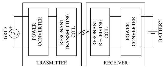
Figure 1.
WBC systems schematics.
The power converter in the transmitter stage includes a Power Factor Correction circuit (PFC) and a High-Frequency Inverter (HFI). The role of the PFC is to convert grid voltage into dc voltage while maintaining power factor unity, and HFI converts this dc voltage into ac voltage at a high frequency suitable for the WBC system, whose output voltage magnitude can be controlled by the phase shift technique. In the receiver stage, the power converter converts the ac voltage induced in the receiver coil into the dc voltage needed to charge the EV battery.
For better efficiency and smaller power supply sizing, the WBC system employs the Compensation Network (CN) along with its coupling coil [8,9]. In the simplest arrangements, the CN is a capacitor connected to the coils that resonates with the coil inductance at the supply frequency. Depending upon the different combinations of the coils, there are four fundamental topologies possible, such as series–series (SS), series–parallel (SP), parallel–series (PS), and parallel–parallel (PP) [10,11,12,13,14,15,16,17,18].
Different architectures are proposed for receiver power circuitry together with parallel compensation [19,20] proposed, where the power conversion circuitry of the receiver includes a diode rectifier to supply the load with a direct voltage and resorts to different solutions for the adjustment of the voltage amplitude; research [21,22] provide the control of the AC voltage before applying it to the diode rectifier for secondary parallel compensation; and [23,24,25] use a diode rectifier cascaded by a buck converter. The most popular technique for a WBC receiver is to charge the battery in a straightforward manner with the diode rectifier or through a chopper and control the voltage of the power source in the transmitter to adjust the power absorbed by the battery. Based on the abovementioned different charging arrangements, this paper compares two types of arrangements, referred to here as arrangements #1 and #2, respectively. Arrangement #1 charges the battery without the control rectifier current/voltage, while Arrangement #2 charges the battery with the chopper, keeping its input voltage constant. The paper performs this analysis considering the SP compensation topology and cost estimation.
The paper is organized as follows: Section 2 briefly describes the operation of a battery-charging process and finds some basic equations for SP topology. Section 3 introduces and determines FOMs (figures of merit) for the SP topology. Section 4 examines the operation of both arrangements. Section 5 discusses the effect of the amplitude of the chopper input voltage on FOMs. Section 6 include the experimental details and results. Section 7 concludes the paper.
Throughout the paper, upper-case symbols with a superimposed bar represent the phasor relevant to the sinusoidal quantities, and their rms value is represented by an upper-case symbol.
2. WBC Background
2.1. Battery Charging
Figure 2 shows the two sequential modes of EV battery charging, such as Constant Current (CC) and Constant Voltage (CV). Here, IB, VB, RB, and PB are assigned for battery current, voltage, resistance, and power, respectively. Battery resistance is defined as the ratio of battery voltage and current. Along with this, Ico and Vco are the cutoff current and voltage, and N is the point of transition from CC to CV mode. For the sake of keeping the study simple, an assumption is made that the battery voltage in CC mode is in a linear charging profile. All the parameters in Figure 2, such as current, voltage, resistance, and power, are normalized. The normalization is carried out as follows: (i) current is normalized to the CC mode current ICC; (ii) voltage is normalized to the maximum battery voltage VM; (iii) resistance is normalized to the resistance at point N, equal to the ratio of VM and ICC and is denoted by RN; and (iv) power is normalized to the power at point N, given by the product of VM and ICC and is denoted as PN. It is observed that the battery resistance in CC mode increased from Rl, which is the ratio of voltage and current at the beginning of CC mode, to RF, which is the ratio of VM and ICO through RN. Also, battery power increases from PI to PN and then decreases to PF. Resistance RB as a function of PB, in CC and CV modes, is represented as
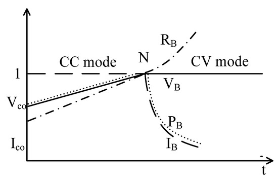
Figure 2.
Battery-charging profile: normalized voltage as in solid line, normalized current as in dashed line, normalized power as in dotted line, and normalized resistance as in dashed-dotted line.
2.2. Analysis of SP Topology
Figure 3 shows the series–parallel topology for the WBC system. The symbols in Figure 3 are assigned as follows: (i) is the power source voltage; (ii) and are the transmitter and receiver side currents; (iii) CT and CR are the transmitter and receiver resonant capacitors; (iv) and are the transmitter and receiver coils terminal voltages; (v) LT and LR are the transmitter and receiver coils inductances; (vi) rT and rR are the transmitter and receiver coils parasitic resistances; (vii) and are the voltage induced in the transmitter and receiver coils due to the effect of mutual inductance; (viii) and are the receiver-side capacitor current and load current; and (ix) RL and are the load resistance and voltage across RL. The induced voltages and are given by
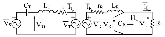
Figure 3.
SP resonant topology WBC circuit diagram.
Here, M and ω are the mutual inductance between the coils and the WBC supply angular frequency. Figure 4 shows the phasor diagram for SP resonant topology, where , are shown orthogonal to and respectively, as given in (2).
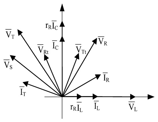
Figure 4.
Phasor diagram for SP resonant topology.
It is obvious from Figure 3 that the receiver current is the phasor sum of the load current and the current in the receiving resonant capacitor and is given as
Since and are in the same phase, then and are orthogonal to each other as is equal to . Replacing with , in Equation (3), then is represented in (4) as
By applying KVL in the Figure 3 receiving-side of the WBC circuit, we get
Equation (5) can further be simplified by using (4), which can be represented in Equation (6) as
Rearranging (2) using (6) expressions for is obtained as
Doing some manipulation in Figure 3 and using (2) and (7), the expression for is
3. FOMs and Their Calculation
3.1. FOMs Introduction
The circuit mentioned in Figure 3 is used to calculate the FOMs. They are calculated under the assumption of neglecting the circuitry losses between the battery and the receiver. Hence, the power absorbed by the battery, denoted by PB, coincides with the power entering the load resistance. Five FOMs such as overall efficiency η, Power Transfer Ratio (PTR), Receiver Efficiency (RE), Power Source Sizing Factor (PSSF), and Receiver Coil Sizing Factor (RCSF), are considered and are defined as follows:
Here, PS is the power source output power, PR is the active power transferred to the receiver, AS is the power source sizing power, and AR is the sizing power of the receiving coil. Sizing powers AS and AR are defined as
where max represents the maximum of the specified quantity in the battery-charging process. It should be noted that PSSF and RCSF are the measures of cost and volume of the WBC system as a function of nominal power absorbed by the battery. Similarly, the detail power-sizing factor of the transmitting coil is expressed in Appendix A.
3.2. FOMs Calculation
Taking into account the first three FOMs from (9) to (11), they can be expressed as
where and are the losses associated with the transmitter and receiver and . Substituting the respective current in (16)–(18) with (4) and (7) and using the relation RL = VL/IL, one can achieve
Maximum RE using (21) is obtained for
and it is given by
Expression (22) states that RL,RE max is not dependent on battery parameters and depends on coil parameters; the same happens for REmax.
PSSF and RCSF can be simplified by neglecting the significance of parasitic resistance in the coils. By simplifying (7) and (8) as
PSSF is given as
The voltage across the receiving coil terminals is
Substituting (4) and (7) into (27), it is found that
From (4) is
RCSF is expressed as
3.3. WBC Arrangements #1
The circuitry of WBC arrangement #1 is drawn in Figure 5. Due to the presence of LDC, CDC, and LF as low-pass filters, the current will be a square wave and sinusoidal. Direct current through the battery will be its peak value, and direct voltage across the battery will coincide with its average value of rectified .
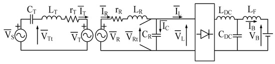
Figure 5.
WBC arrangement #1 circuitry.
It is to be noted that and are in phase, and hence the receiver considers the WBC load as the resistive load. This resistive load, as mentioned previously, is the load resistance and is given as
The load voltage and current rms values in terms of VB and IB are
Substituting (32) and (33) into (29) RL is obtained as
Due to the presence of a constant term in (34), it is clear that load resistance is proportional to the battery resistance.
3.4. WBC Arrangements #2
Figure 6 draws the circuitry for WBC arrangement #2. In this arrangement, let the voltage across CDC be at value VDC VM and kept constant in any charging condition. Then the chopper duty cycle δ is given as
During CC mode, δ varies from Vco/VDC to VM/VDC, whilst in CV mode, it remains constant and is equal to VM/VDC. Due to the duty cycle, the resistance seen by the capacitor CDC is
Substituting (35) in (36) and replacing RB in (34) with RDC,B load resistance becomes

Figure 6.
WBC arrangement #2 circuitry.
Figure 6.
WBC arrangement #2 circuitry.

4. Arrangement Comparison
4.1. Study Case
The study case for this paper is a prototype developed to charge an electric city-car in [23]. Battery and WBC data are listed in Table 1.

Table 1.
Battery and WBC system data.
4.2. PTR, RE, and Efficiency
Figure 7, Figure 8 and Figure 9 plot the PTR, RE, and efficiency with respect to the PB normalized to PN. In these plots, curves ABA*C belong to arrangement #1, and curves A*BC belong to arrangement #2. The simulation has been carried out in the MATLAB/Simulink environment. The FOMs expressions are extracted as in (19)–(21), where the value of RL has been chosen as (34) and (37) for arrangement #1 and arrangement #2, respectively.
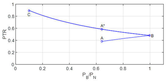
Figure 7.
PTR for WBC arrangement #1 and #2.
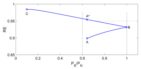
Figure 8.
RE for WBC arrangements #1 and #2.
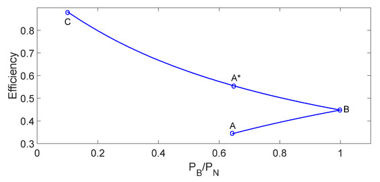
Figure 9.
Efficiency for WBC arrangements #1 and #2.
For arrangement #1, load resistance RL in (19)–(21) is expressed in terms of PB by substituting (1) into (34), while for arrangement #2, it is done by substituting (1) into (37). Analysis of arrangement #2 is carried out by setting VDC at VM.
4.3. Arrangement #1
PTR: CC mode starts at PB = 360 W, where PTR is 0.38, shown as point A in Figure 7. IT can be assumed to be maximum and constant as (24), and so the constant is the loss associated with it. IR, as given in (30), increases due to an increase in VL and so increases losses associated with it. An increase in loss associated with rR does not account for with respect to an increase in PB, and hence PTR increases to point B shown in Figure 7.
CV mode starts from PB = 560 W as point B, as shown in Figure 7. By comparing (24) and (29) and considering the data of Table 1, it is found that IT is approximately four times greater than that of IR, and hence loss associated with IT is much higher than that of IR. IT mitigates the impact of IR, which causes an increase in PTR and reaches a value of 0.89 at point C at the completion of CV mode.
RE: During CC mode, starting from point A shown in Figure 8, and having RE close to 0.9, a small increase in loss associated with rR (as discussed in the case of PTR) is compensated by the increase in PB that increases RE to 0.93 at the completion of mode, shown as point B.
In CV mode, starting from point B in Figure 8, RE increases due to the fact that PB decreases linearly to IL while losses are associated with IR with the power of two. RE reaches its maximum at PB = 60.3 W and starts mitigating onwards due to the influence of IC over IL.
Efficiency: During CC mode, as explained for PTR and RE, variation of efficiency, as shown in Figure 8, from points A to B is expected. In CV mode, losses in rT conquer the losses in rR due to the fact that IT is approximately four times that of IT, and hence the curve of efficiency follows PTR and reaches point C at the completion of CV mode through point A*.
4.4. Arrangement #2
The urge of this arrangement is to have DC link voltage constant during the whole charging process. Thus, charging during CV mode will be the same as arrangement #1 for the same value of DC-link voltage. This, in the case of PTR, RE, and efficiency, will vary from point B to C through A* as in arrangement #1.
During CC mode, PB increases from PI to PN, keeping VB constant as VM, and current IB falls to such that
and reaches ICC at the completion of CC mode. So, the CC mode for this arrangement will follow the CV mode of arrangement #1, which will move from point A* to point B for PTR, RE, and efficiency.
PTR: During CC mode, variation of PTR as a function of PB is shown in Figure 7, which starts from point A* at PB = 360 W and diminishes due to the fact that the effect of rT losses prevails on the effect of rR losses as well as an increase in PB and reaches point B at the completion of CC mode.
RE: CC mode starts from point A’ as shown in Figure 8. During CC mode, IR increases with IL with its power of two, while the increase in PB is linear with IL, so losses associated with rR overcome the increase in PB, causing a decrease in RE and reaching point B at the completion of CC mode.
Efficiency: CC mode starts from point A*, as shown in Figure 9. During CC mode, IR and IT both increase with IL with the power of two while the increase in PB is linear, so losses associated with rT and rR prevail on the increase in PB, causing a decrease in it and reaching point B at the completion of CC mode.
4.5. Efficiency Comparison
Efficiency during CC mode is higher for arrangement #2 because (1) IT is more or less constant by (24), which in practice is not so and varies slightly due to the presence of rR, but for simplicity, it can be neglected. For arrangement #1, IT is maximum, and so are the losses associated with it, but for arrangement #2, IT starts with IL, which corresponds to IB as and reaches its maximum where IB is ICC, and so, loss associated with rT is always less in this arrangement with reference to arrangement #1, which coincides with the completion of CC mode. (2) In this mode, the effect of the current IC is very small, so the IR and losses associated with rR using the above argument are always greater for arrangement #1 than arrangement #2 and coincide at the completion of CC mode.
4.6. PSSF and RCSF
From (26), it can be observed that PSSF for both arrangements will be maximum at point N on the battery-charging profile. Replacing VB and IB with VM and ICC from (32) and (33) PSSF is calculated as 9.33 and 9.54 if parasitic resistances are considered. The excess PSSF is due to the voltage drop across rT and rR.
Expression (30) clarifies that the RCSF for both arrangements will be maximum at point N on the battery-charging profile. Using (32) and (33) and replacing VB and IB with VM and ICC, RCSF is calculated as 1 and remains the same even if parasitic resistance is considered.
5. Effect on the Chopper
In order to select a convenient chopper input voltage VDC for arrangement #2, PTR, RE, and efficiency are investigated for three different values of VDC as VM, 1.2 VM, and 1.4 VM. Figure 10, Figure 11 and Figure 12 plot the PTR, RE, and efficiency with respect to the PB normalized to PN by MATLAB/Simulation.
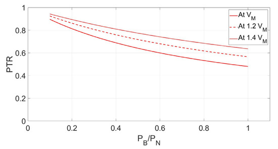
Figure 10.
PTR for WBC arrangement #2 with VDC = VM, 1.2 VM, and 1.4 VM.
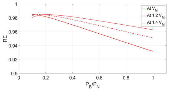
Figure 11.
RE for WBC arrangement #2 with VDC = VM, 1.2 VM, and 1.4 VM.
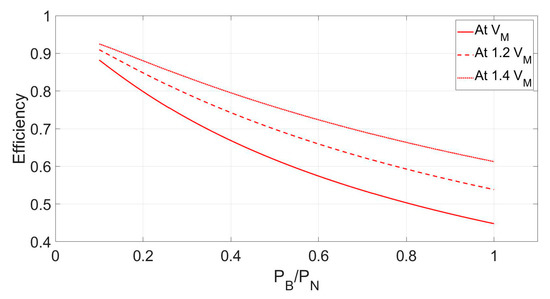
Figure 12.
Efficiency for WBC arrangement #2 with VDC = VM, 1.2 VM, and 1.4 VM.
PTR: Figure 10 shows that PTR increases with the higher value of VM, which is due to the fact that for a given value of PB, IL is less for VDC > VM, and so are the values of IT and IR. From (24) and (29), it is clear that the decrease in IT is significantly higher than IR. Due to this, losses associated with rT dominate over losses associated with rR.
RE: Figure 11 shows that for the higher value of PB, RE increases with VDC because, for a given value of PB, since VL is high current IL is low, and so losses associated with rR will be less, which results in the increase of RE. For the lower value of PB, IC predominates over IL, which is high for VDC > VM and causes a decrease in RE.
Efficiency: Figure 12 shows that efficiency increases with the increase of VDC due to the fact that, for the higher value of VDC, current IL is low, and IT and IR will also be lower. For the lower value of IT and IR, losses associated with them will be low, which results in an increase in efficiency.
PSSF and RCSF: Using (26) PSSF for VDC = VM, 1.2 VM and 1.4 VM are calculated as 9.54, 9.59, and 9.64, respectively, by considering the effect of parasitic resistances. The RCSF from (30) for the same values of VDC is 1, 1.21, and 1.41, respectively.
6. Experimental Analysis
The theoretical finding for efficiency is checked by an experiment executed on SP resonant WBC with the characteristics reported in Table 1. The experimental setup for WBC systems is shown in Figure 13. The variable resistor is used in place of the battery for both arrangements. The first set of tests is carried out by adjusting the voltage of the power source for the operation of arrangement #1. Operation of arrangement #2 has been carried out on VDC as VM, 1.2 VM, and 1.4 VM. The experimental results are plotted in Figure 14 and Figure 15, which perfectly match the theoretical findings.
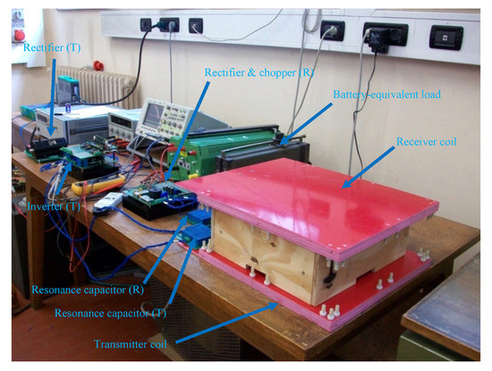
Figure 13.
WBC prototype.
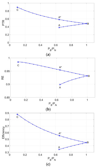
Figure 14.
Experimental results for (a) PTR, (b) RE, and (c) efficiency for WBC arrangements #1 and #2.
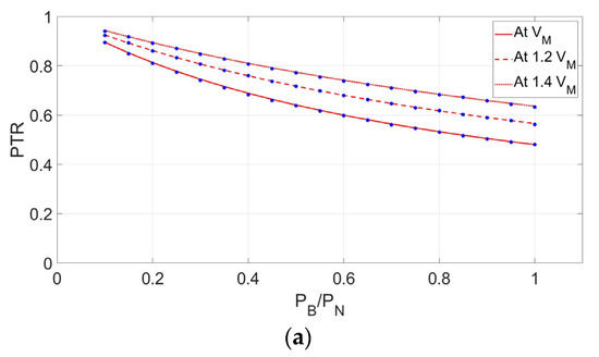
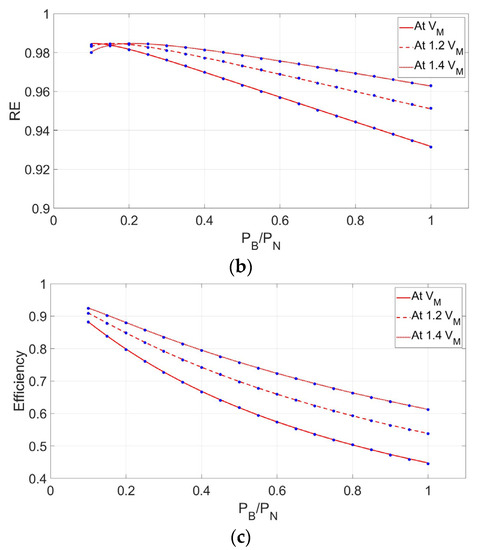
Figure 15.
Experimental results for (a) PTR, (b) RE, and (c) efficiency for WBC arrangement #2 with VDC = VM, 1.2 VM, and 1.4 VM.
Figure 14a–c are plots of the PTR, RE, and efficiency with respect to the PB normalized to PN. In these results, the blue line represents the simulated results, and the blue dot represents the experiment results, which almost overlap the simulation results. In these plots, curves ABA*C belong to arrangement #1 in both CC and CV modes, and curves A*BC belong to arrangement #2, whose charging during CV mode will be the same as arrangement #1 for the constant value of DC-link voltage during the whole charging process. This, in the case of PTR, RE, and efficiency, will vary from point B to point C through A* as in arrangement #1. While in the case of the CC mode of arrangement #2 the PTR, RE, and efficiency, will vary from point A* to point B. PB increases from PI to PN keeping VB constant as VM, current IB falls to and reaches ICC at the completion of CC mode.
Figure 15a–c are plots of the PTR, RE, and efficiency with respect to the PB normalized to PN. In these results, the red line represents the simulated results, and the blue dot represents the experiment results. Those are almost identical to simulation results. To select a convenient chopper input voltage VDC for arrangement #2 PTR, RE and efficiency are investigated for three different values of VDC as VM, 1.2 VM, and 1.4 VM. It is found that, the PTR, RE, and efficiency increase with a higher value of VM, which is due to the fact that for a given value of PB, IL is less for VDC > VM.
The components of the two different arrangements of the WBC are quite similar. These components are purchased from retailers in a very small number of samples or have been designed and manufactured on purpose; consequently, the price of the prototype is much higher than that of a mass-produced system. The total cost for the prototype in arrangement #1 was equal to EUR 5800, as mentioned in [26,27]. However, WBC arrangement #2 is a bit more expensive than WBC arrangement #1, as arrangement #2 has an extra set of DC-DC converters and a respective controller to regulate the current for battery charging.
7. Conclusions
The paper deals with two different arrangements for WBC. The first charging arrangement charges the battery without using a chopper and controls rectifier voltage/current based on the battery-charging profile, while the second charging arrangement charges the battery with the chopper. Based on their performance on five FOMs as measured by efficiency, PTR, RE, PSSF, and RCSF, the second arrangement is found to be more favorable for WBC. To select the most convenient chopper input voltage, three different voltages were considered, with a higher value of the chopper input voltage found to be most suitable for WBC, apart from a small compromise with PSSF and RCSF. However, in terms of cost estimation, arrangement #2 is costly compared to arrangement #1.
Author Contributions
Conceptualization, A.K., R.K.J. and M.B.; methodology A.K., R.K.J. and M.B.; software, A.K. and R.K.J.; validation, A.K. and R.K.J.; formal analysis, A.K. and R.K.J.; investigation, A.K. and R.K.J.; resources A.K., R.K.J., M.B., C.B.K., S.J. and G.M.; data curation, A.K., R.K.J., M.B., C.B.K., S.J., G.M. and A.S.; writing—original draft preparation, A.K., R.K.J., M.B., C.B.K., S.J., G.M. and A.S.; writing—review and editing, A.K., R.K.J., M.B., C.B.K., S.J., G.M. and A.S.; visualization, A.K., R.K.J., M.B., C.B.K., S.J., G.M. and A.S.; supervision, A.K., R.K.J. and M.B. All authors have read and agreed to the published version of the manuscript.
Funding
This research received no external funding.
Data Availability Statement
Most of the data and the results are reported in the paper. Additional data can be requested from the corresponding author.
Conflicts of Interest
The authors declare no conflict of interest.
Nomenclature
| WBCSs | Wireless Battery Charging Systems |
| PFC | Power Factor Correction |
| HFI | High-Frequency Inverter |
| CN | Compensation Network |
| EV | Electrical Vehicle |
| SS | Series–Series |
| SP | Series–Parallel |
| FOM | Figure of Merit |
| CC | Constant Current |
| CV | Constant Voltage |
| IB | Battery Current |
| VB | Battery Voltage |
| RB | Battery resistance |
| PB | Battery power |
| Ico | Cutoff current |
| Vco | Cutoff voltage |
| ICC | Normalized current in CC mode |
| VM | Normalized maximum voltage of battery |
| RN | Normalized resistance at point N |
| PN | Normalized power at point N |
| Power source voltage | |
| Transmitter-side current | |
| Receiver-side current | |
| CT | Transmitter-side resonant capacitor |
| CR | Receiver-side resonant capacitor |
| Transmitter coil terminal voltage | |
| Receiver coil terminal voltage | |
| rT | Transmitter coil parasitic resistance |
| rR | Receiver coil parasitic resistance |
| Transmitter coil induce voltage | |
| Receiver coil induce voltage | |
| Receiver-side capacitor current | |
| Load current | |
| RL | Load resistance |
| Voltage across RL | |
| M | Mutual inductance |
| ω | Supply angular frequency |
| η | Efficiency |
| PTR | Power Transfer Ratio |
| RE | Receiver Efficiency |
| PSSF | Power Source Sizing Factor |
| RCSF | Receiver Coil Sizing Factor |
| PS | Power source output power |
| PR | Power transfer to receiver |
| AS | Power source sizing power |
| AR | Receiver coil sizing power |
| Loss of transmitter coil | |
| Loss of receiver coil | |
| LDC | Low pass filter inductor |
| CDC | Low pass filter capacitor |
| VDC | Voltage across CDC in arrangement #2 |
| δ | Chopper duty cycle |
Appendix A
The power-sizing factor of the receiving coil is given by (15), where is the maximum of (28). Similarly, the power-sizing factor of the transmitting coil is expressed as
From the circuit diagram of Figure 3, the voltage across the transmitting coil terminals is
Using (2), (4), and (7) rms values of is given as
The maximum of is again achieved at point N of the charging profile, where both and get the maximum values. Using (A1), (A2), (24), and (15), (28), (29), the relationship between and can be written for point N as
Equation (A4) shows that the relationship between the sizing factors of the transmitting and receiving coils depend on the inductive parameters of the coils, receiving a stage capacitor and battery resistance at point N.
References
- Kumar, A.; Singh, A.R.; Meena, N.K.; Deng, Y.; He, X.; Kumar, P.; Bansal, R.C. Design and Evaluation of Microgrids Based on Renewable Energy Technologies with a Perspective of Sustainable Development. Bansal Handb. Renew. Energy Technol. Syst. 2021, 385–415. [Google Scholar] [CrossRef]
- Rangu, S.K.; Lolla, P.R.; Dhenuvakonda, K.R.; Singh, A.R. Recent trends in power management strategies for optimal operation of distributed energy resources in microgrids: A comprehensive review. Int. J. Energy Res. 2020, 44, 9889–9911. [Google Scholar] [CrossRef]
- Vázquez-Leal, H.; Gallardo-Del-Angel, A.; Castañeda-Sheissa, R.; González-Martínez, F.J. The phenomenon of wireless energy transfer: Experiment and philosophy. In Wireless Power Transfer—Principles and Engineering Explorations; Kim, K.Y., Ed.; IntechOpen: London, UK, 2012. [Google Scholar]
- Bertoluzzo, M.; Mude, K.N.; Buja, G. Preliminary investigation on contactless energy transfer for electric vehicle battery recharging. In Proceedings of the 2012 IEEE 7th International Conference on Industrial and Information Systems (ICIIS), Madras, India, 6–9 August 2012; pp. 1–6. [Google Scholar]
- Buja, G.; Jha, R.K.; Bertoluzzo, M.; Naik, M.K. Analysis and comparison of two wireless battery charger arrangements for electric vehicles. Chin. J. Electr. Eng. 2015, 1, 50–57. [Google Scholar]
- Tuttle, D.P.; Baldick, R. The evolution of plug-in electric vehicle grid interactions. IEEE Trans. Smart Grid 2012, 3, 500–505. [Google Scholar] [CrossRef]
- Kaneko, Y.; Abe, S. Technology trends of wireless power transfer systems for electric vehicle and plug-in hybrid electric vehicle. In Proceedings of the 2013 IEEE 10th International Conference on Power Electronics and Drive Systems (PEDS), Kitakyushu, Japan, 22–25 April 2013; pp. 1009–1014. [Google Scholar]
- Mude, K.N.; Bertoluzzo, M.; Buja, G. Design of contactless battery charger for electric vehicle. In Proceedings of the African Electrical Technology Conference, Pamplemousses, Mauritius, 12–15 May 2013; pp. 1099–1104. [Google Scholar]
- Zhou, W.; Ma, H. Design considerations of compensation topologies in ICPT system. In Proceedings of the APEC 07-Twenty-Second Annual IEEE Applied Power Electronics Conference and Exposition, Anaheim, CA, USA, 25 February–1 March 2007; pp. 985–990. [Google Scholar]
- Zhang, W.; Wong, S.-C.; Tse, C.K.; Chen, Q. Analysis and comparison of secondary series- and parallel-compensated inductive power transfer systems operating for optimal efficiency and load-independent voltage-transfer ratio. IEEE Trans. Power Electron. 2014, 29, 2979–2990. [Google Scholar] [CrossRef]
- Bertoluzzo, M.; Buja, G.; Mude, K.N. Characteristic Evaluation of Wireless Battery Chargers for Electric Vehicles. Electromotion 2013, 20, 103–108. [Google Scholar]
- Li, W.; Zhao, H.; Li, S.; Deng, J.; Kan, T.; Mi, C.C. Integrated LCC Compensation Topology for Wireless Charger in Electric and Plug-in Electric Vehicles. IEEE Trans. Ind. Electron. 2015, 62, 4215–4225. [Google Scholar] [CrossRef]
- Pantic, Z.; Bhattacharya, S.; Lukic, S. Optimal resonant tank design considerations for primary track compensation in inductive power transfer systems. In Proceedings of the IEEE Energy Conversion Congress and Exposition (ECCE), Atlanta, GA, USA, 2-16 September 2010; pp. 1602–1609. [Google Scholar]
- Bailian, N.; Chung, C.Y.; Chan, H.L. Design and comparison of parallel and series resonant topology in wireless power transfer. In Proceedings of the IEEE (ICIEA), Melbourne, Australia, 19–21 June 2013; pp. 1832–1837. [Google Scholar]
- Pantic, Z.; Lukic, S. Framework and topology for active tuning of parallel compensated receivers in wireless power transfer systems. IEEE Trans. Power Electron. 2012, 99, 1–10. [Google Scholar]
- Kumar, A.; Bertoluzzo, M.; Jha, R.K.; Sagar, A. Analysis of Losses in Two Different Control Approaches for S-S Wireless Power Transfer Systems for Electric Vehicle. Energies 2023, 16, 1795. [Google Scholar] [CrossRef]
- Keeling, N.A.; Covic, G.A.; Boys, J.T. A Unity-Power-Factor IPT Pickup for High-Power Applications. IEEE Trans. Ind. Electron. 2010, 57, 744–751. [Google Scholar] [CrossRef]
- Chao, Y.-H.; Shieh, J.-J.; Pan, C.-T.; Shen, W.-C.; Chen, M.-P. A Primary-Side Control Strategy for Series-Parallel Loosely Coupled Inductive Power Transfer Systems. In Proceedings of the IEEE Conference on Industrial Electronics and Applications (ICIEA), Harbin, China, 23–25 May 2007; pp. 2322–2327. [Google Scholar]
- Chen, J.; Maksimovic, D.; Erickson, R. Buck-boost PWM converters having two independently controlled switches. In Proceedings of the IEEE Power Electronics Specialists Conference (PESC), Vancouver, BC, Canada, 17–21 June 2001; Volume 2, pp. 736–741. [Google Scholar]
- Yao, C.; Ruan, X.; Cao, W.; Chen, P. A Two-Mode Control Scheme with Input Voltage Feed-Forward for the Two-Switch Buck-Boost DC–DC Converter. IEEE Trans. Power Electron. 2014, 29, 2037–2048. [Google Scholar] [CrossRef]
- Colak, K.; Bojarski, M.; Asa, E.; Czarkowski, D. A constant resistance analysis and control of cascaded buck and boost converter for wireless EV chargers. In Proceedings of the IEEE Applied Power Electronics Conference and Exposition (APEC), Charlotte, NC, USA, 15–19 March 2015; pp. 3157–3161. [Google Scholar]
- Wu, H.H.; Covic, G.A.; Boys, J.T.; Hu, A.P. A 1 kW inductive charging system using AC processing pickups. In Proceedings of the IEEE Industrial Electronics and Applications (ICIEA), Beijing, China, 21–23 June 2011; pp. 1999–2004. [Google Scholar]
- Sagar, A.; Kumar, A.; Bertoluzzo, M.; Jha, R.K. Analysis and Design of a Two-winding Wireless Power Transfer System with Higher System Efficiency and Maximum Load Power. In Proceedings of the IECON 2022—48th Annual Conference of the IEEE Industrial Electronics Society, Brussels, Belgium, 18–21 October 2022; pp. 1–6. [Google Scholar]
- Sagar, A.; Bertoluzzo, M.; Kumar, A. Analysis and Comprehensive Comparison of Wireless Power Transfer System Using SS and SP topology for Electric Vehicle Charging. In Proceedings of the 2023 International Conference on Computational Intelligence, Communication Technology and Networking (CICTN), Ghaziabad, India, 20–21 April 2023; pp. 235–240. [Google Scholar]
- Haller, S.; Alam, M.F.; Bertilsson, K. Reconfigurable Battery for Charging 48 V EVs in High-Voltage Infrastructure. Electronics 2022, 11, 353. [Google Scholar] [CrossRef]
- Buja, G.; Bertoluzzo, M.; Mude, K.N. Design and Experimentation of WPT Charger for Electric City-Car. IEEE Trans. Ind. Electron. 2015, 62, 7436–7447. [Google Scholar] [CrossRef]
- Bertoluzzo, M.; Giacomuzzi, S.; Kumar, A. Design of a Bidirectional Wireless Power Transfer System for Vehicle-to-Home Applications. Vehicles 2021, 3, 406–425. [Google Scholar] [CrossRef]


Disclaimer/Publisher’s Note: The statements, opinions and data contained in all publications are solely those of the individual author(s) and contributor(s) and not of MDPI and/or the editor(s). MDPI and/or the editor(s) disclaim responsibility for any injury to people or property resulting from any ideas, methods, instructions or products referred to in the content. |
© 2023 by the authors. Licensee MDPI, Basel, Switzerland. This article is an open access article distributed under the terms and conditions of the Creative Commons Attribution (CC BY) license (https://creativecommons.org/licenses/by/4.0/).