

Optically Transparent Dual-Band Metamaterial Absorber Using Ag Nanowire Screen-Printed Second-Order Cross-Fractal Structures


Abstract
1. Introduction
2. Design and Analysis
2.1. Design of the Second-Order Cross-Fractal-Structured MMA
2.2. Analysis of the Second-Order Cross-Fractal-Structured MMA
2.2.1. Reflection Coefficient, Absorptivity, and Normalized Impedance
2.2.2. Analysis of Electromagnetic Absorption Mechanism
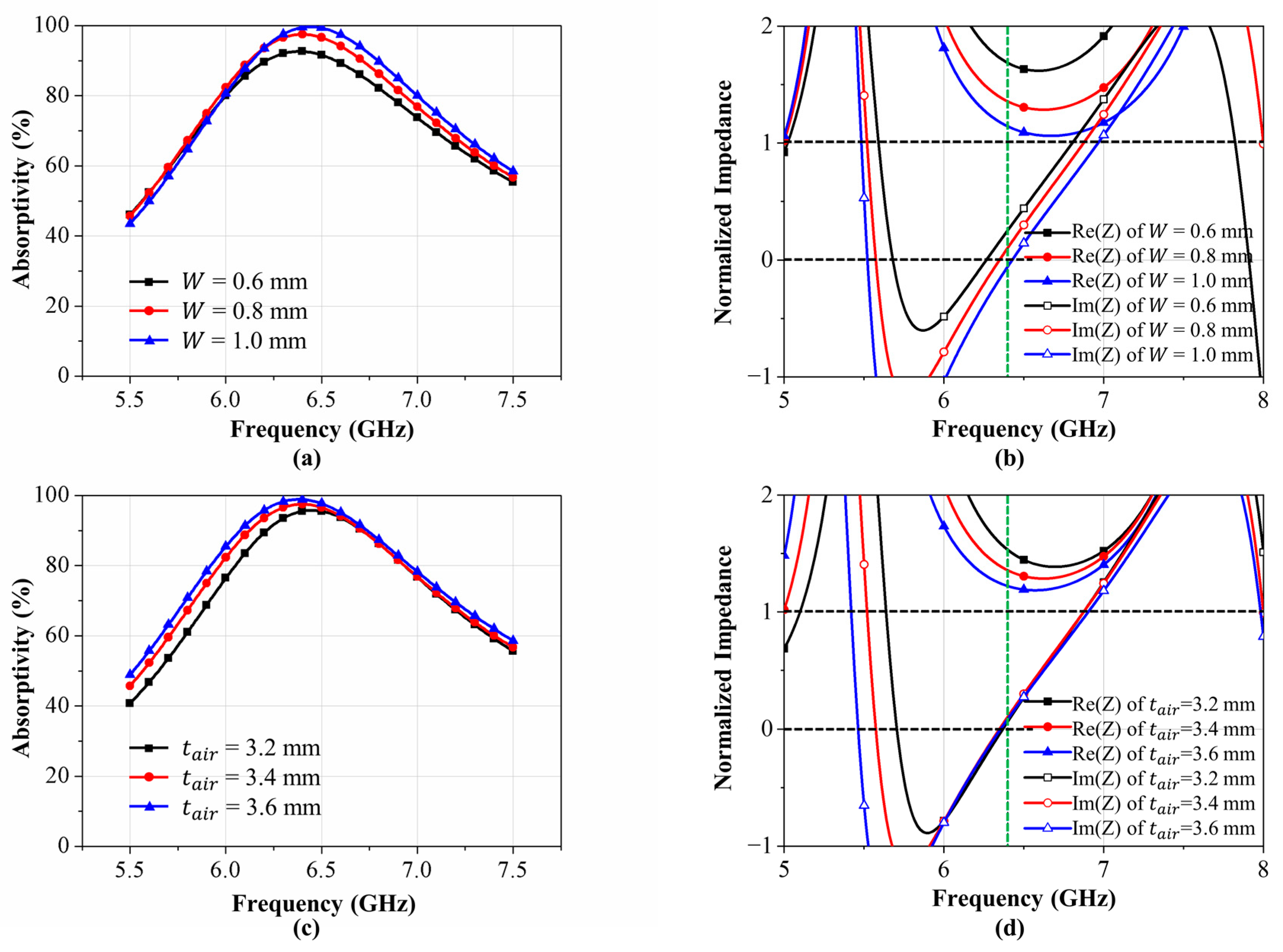
2.2.3. Parametric Study
3. Fabrication
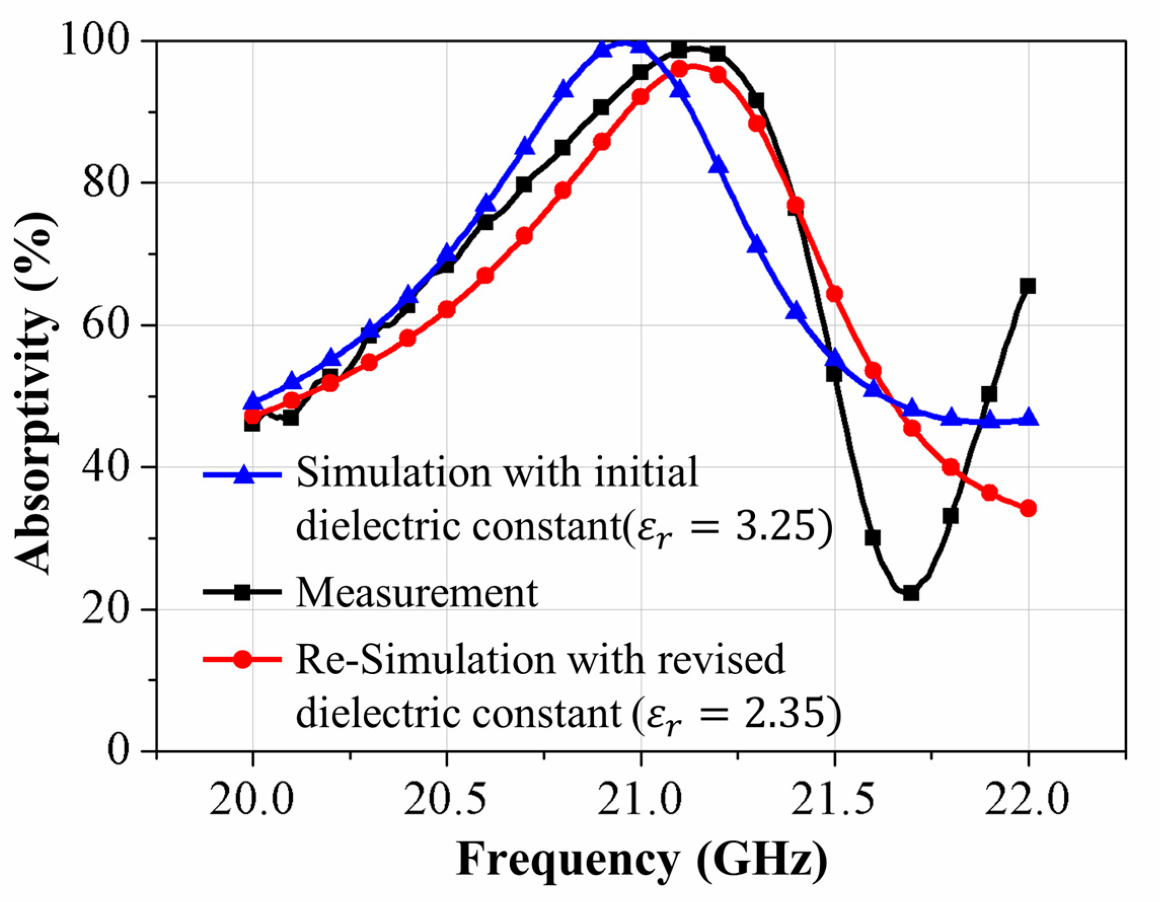
4. Results and Discussion
5. Conclusions
Author Contributions
Funding
Data Availability Statement
Conflicts of Interest
References
- Sun, H.; Gu, C.; Chen, X.; Li, Z.; Liu, L.; Xu, B.; Zhou, Z. Broadband and Broad-Angle Polarization-Independent Metasurface for Radar Cross Section Reduction. Sci. Rep. 2017, 7, 40782. [Google Scholar] [CrossRef]
- Marra, F.; Lecini, J.; Tamburrano, A.; Pisu, L.; Sarto, M.S. Electromagnetic Wave Absorption and Structural Properties of Wide-Band Absorber Made of Graphene-Printed Glass-Fibre Composite. Sci. Rep. 2018, 8, 12029. [Google Scholar] [CrossRef]
- Tong, X. Advanced Materials and Design for Electromagnetic Interference Shielding, 1st ed.; Taylor & Francis Group: Boca Raton, FL, USA, 2008. [Google Scholar]
- Mishra, R.K.; Gupta, R.D.; Datar, S. Metamaterial Microwave Absorber (MMA) for Electromagnetic Interference (EMI) Shielding in X-Band. Plasmonics 2021, 16, 2061–2071. [Google Scholar] [CrossRef]
- Fante, R.L.; Mccormack, M.T. Reflection Properties of the Salisbury Screen. IEEE Trans. Antennas Propag. 1988, 36, 1443–1454. [Google Scholar] [CrossRef]
- Du Toit, L.J. The Design of Jauman Absorbers. IEEE Antennas Propag. Mag. 1994, 36, 17–25. [Google Scholar] [CrossRef]
- Landy, N.I.; Sajuyigbe, S.; Mock, J.J.; Smith, D.R.; Padilla, W.J. Perfect Metamaterial Absorber. Phys. Rev. Lett. 2008, 100, 207402. [Google Scholar] [CrossRef] [PubMed]
- Li, K.; Lu, H.; Bi, M.; He, W.; Qi, L.; Zhou, Z.; Weng, X. Multi-Band Polarization-Insensitive Metamaterial Absorber for Microwave Based on Slotted Structure and Magnetic Rubber. Polymers 2022, 14, 1576. [Google Scholar] [CrossRef] [PubMed]
- Ma, Y.; Chen, Q.; Grant, J.; Saha, S.C.; Khalid, A.; Cumming, D.R.S. A Terahertz Polarization Insensitive Dual Band Metamaterial Absorber. Opt. Lett. 2011, 36, 945. [Google Scholar] [CrossRef] [PubMed]
- Zhang, N.; Zhou, P.; Cheng, D.; Weng, X.; Xie, J.; Deng, L. Dual-Band Absorption of Mid-Infrared Metamaterial Absorber Based on Distinct Dielectric Spacing Layers. Opt. Lett. 2013, 38, 1125. [Google Scholar] [CrossRef] [PubMed]
- Soheilifar, M.R.; Sadeghzadeh, R.A. Design, Fabrication and Characterization of Stacked Layers Planar Broadband Metamaterial Absorber at Microwave Frequency. AEU Int. J. Electron. Commun. 2015, 69, 126–132. [Google Scholar] [CrossRef]
- Wen, Q.Y.; Zhang, H.W.; Xie, Y.S.; Yang, Q.H.; Liu, Y.L. Dual Band Terahertz Metamaterial Absorber: Design, Fabrication, and Characterization. Appl. Phys. Lett. 2009, 95, 241111. [Google Scholar] [CrossRef]
- Lee, H.M.; Lee, H.S. A Method for Extending the Bandwidth of Metamaterial Absorber. Int. J. Antennas Propag. 2012, 2012, 859429. [Google Scholar] [CrossRef]
- Ajewole, B.; Kumar, P.; Afullo, T. I-Shaped Metamaterial Using SRR for Multi-Band Wireless Communication. Crystals 2022, 12, 559. [Google Scholar] [CrossRef]
- Islam, S.S.; Iqbal Faruque, M.R.; Islam, M.T. Design and Absorption Analysis of a New Multiband Split-S-Shaped Metamaterial. Sci. Eng. Compos. Mater. 2017, 24, 139–148. [Google Scholar] [CrossRef]
- Mandelbrot, B.B.; Wheeler, J.A. The Fractal Geometry of Nature. Am. J. Phys. 1983, 51, 286–287. [Google Scholar] [CrossRef]
- Anguera, J.; Andújar, A.; Jayasinghe, J.; Sameer Chakravarthy, V.V.S.S.; Chowdary, P.S.R.; Pijoan, J.L.; Ali, T.; Cattani, C. Fractal Antennas: An Historical Perspective. Fractal Fract. 2020, 4, 3. [Google Scholar] [CrossRef]
- Bisht, N.; Malik, P.K.; Das, S.; Islam, T.; Asha, S.; Alathbah, M. Design of a Modified MIMO Antenna Based on Tweaked Spherical Fractal Geometry for 5G New Radio (NR) Band N258 (24.25–27.25 GHz) Applications. Fractal Fract. 2023, 7, 718. [Google Scholar] [CrossRef]
- Shan, D.; He, L.; Deng, L.; Luo, H.; Liao, C.; Peng, Y.; Xu, Y.; Huang, S. Comptibility of Optical Transparency and Microwave Absorption in C-Band for the Metamaterial with Second-Order Cross Fractal Structure. Phys. E Low-Dimens. Syst. Nanostructures 2020, 116, 113756. [Google Scholar] [CrossRef]
- Kim, J.; Keun, J.; Yoo, T.; Lim, S. Miniaturization and Bandwidth Enhancement of Fractal-Structured Two-Arm Sinuous Antenna Using Gap Loading with Meandering. Fractal Fract. 2023, 7, 841. [Google Scholar] [CrossRef]
- Paun, M.A.; Nichita, M.V.; Paun, V.A.; Paun, V.P. Minkowski’s Loop Fractal Antenna Dedicated to Sixth Generation (6G) Communication. Fractal Fract. 2022, 6, 402. [Google Scholar] [CrossRef]
- Vallappil, A.K.; Khawaja, B.A.; Rahim, M.K.A.; Uzair, M.; Jamil, M.; Awais, Q. Minkowski–Sierpinski Fractal Structure-Inspired 2 × 2 Antenna Array for Use in Next-Generation Wireless Systems. Fractal Fract. 2023, 7, 158. [Google Scholar] [CrossRef]
- Fan, S.; Song, Y. Bandwidth-Enhanced Polarization-Insensitive Metamaterial Absorber Based on Fractal Structures. J. Appl. Phys. 2018, 123, 085110. [Google Scholar] [CrossRef]
- Munaga, P.; Ghosh, S.; Bhattacharyya, S.; Srivastava, K.V. A Fractal-Based Compact Broadband Polarization Insensitive Metamaterial Absorber Using Lumped Resistors. Microw. Opt. Technol. Lett. 2016, 58, 343–347. [Google Scholar] [CrossRef]
- Jiang, H.; Xue, Z.; Li, W.; Ren, W. Multiband Polarisation Insensitive Metamaterial Absorber Based on Circular Fractal Structure. IET Microw. Antennas Propag. 2016, 10, 1141–1145. [Google Scholar] [CrossRef]
- Fang, S.; Deng, L.; Zhang, P.; Qiu, L.; Xie, H.; Du, J.; Wang, H.; Zhao, H. Dual-Band Metamaterial Absorber with Stable Absorption Performance Based on Fractal Structure. J. Phys. D Appl. Phys. 2022, 55, 095003. [Google Scholar] [CrossRef]
- Peng, Y.; Wang, Q.; Xu, Y.; Shan, D.; He, L.; Cao, Y. Optically Transparent and Mechanically Stretchable Fractal-Structured Wave-Absorbing Metamaterial in Low Frequency Range. J. Alloys Compd. 2023, 961, 171100. [Google Scholar] [CrossRef]
- Nguyen, T.D.; Kim, S.E.; Jung, C.W. Compact, Flexible and Transparent Antenna Using MMF for Conformal Wi-Fi 7 Applications. J. Electr. Eng. Technol. 2023, 18, 4341–4352. [Google Scholar] [CrossRef]
- Nguyen, T.D.; Choi, J.H.; Jung, C.W. Optically Transparent Patch Antennas Using Saltwater for WLAN Applications. J. Electromagn. Eng. Sci. 2022, 22, 609–615. [Google Scholar] [CrossRef]
- Phan, D.T.; Jung, C.W. Transparent Liquid Multiple-Antenna Array with a High Gain and Beam Diversity for UHD TV Applications. J. Electromagn. Eng. Sci. 2022, 22, 186–194. [Google Scholar] [CrossRef]
- Zhang, C.; Cheng, Q.; Yang, J.; Zhao, J.; Cui, T.J. Broadband Metamaterial for Optical Transparency and Microwave Absorption. Appl. Phys. Lett. 2017, 110, 143511. [Google Scholar] [CrossRef]
- Kang, J.; Qu, Z.; Duan, J.; Jing, H.; Hao, J.; Song, C.; Wang, J.; Zhang, B. Multispectral Flexible Ultrawideband Metamaterial Absorbers for Radar Stealth and Visible Light Transparency. Opt. Mater. 2023, 135, 113351. [Google Scholar] [CrossRef]
- Jiang, H.; Yang, W.; Lei, S.; Hu, H.; Chen, B.; Bao, Y.; He, Z. Transparent and Ultra-Wideband Metamaterial Absorber Using Coupled Hexagonal Combined Elements. Opt. Express 2021, 29, 29439. [Google Scholar] [CrossRef]
- Nguyen, T.D.; Lee, Y.; Jung, C.W. Transparent and Flexible Patch Antenna Using MMF for Conformal WiFi-6E Applications. J. Electromagn. Eng. Sci. 2023, 23, 310–317. [Google Scholar] [CrossRef]
- Yoo, Y.; Jeong, H.; Lim, D.; Lim, S. Stretchable Screen-Printed Metasurfaces for Wireless Strain Sensing Applications. Extrem. Mech. Lett. 2020, 41, 100998. [Google Scholar] [CrossRef]
- Hollis, J.S.; Ecker, H.A. Determination of Far-Field Antenna Patterns from Near-Field Measurements. Proc. IEEE 1973, 61, 1668–1694. [Google Scholar] [CrossRef]
- Yoo, M.; Kim, H.K.; Lim, S. Angular- and Polarization-Insensitive Metamaterial Absorber Using Subwavelength Unit Cell in Multilayer Technology. IEEE Antennas Wirel. Propag. Lett. 2016, 15, 414–417. [Google Scholar] [CrossRef]
- Lee, D.; Hwang, J.G.; Lim, D.; Hara, T.; Lim, S. Incident Angle- and Polarization-Insensitive Metamaterial Absorber Using Circular Sectors. Sci. Rep. 2016, 6, 27155. [Google Scholar] [CrossRef] [PubMed]


| Parameter | Dimension (mm) | Parameter | Dimension (mm) |
|---|---|---|---|
| 16.6 | 4.5 | ||
| 0.8 | 0.25 | ||
| 14 | 3.4 |
| Structure Characteristics | Peak Absorption Frequency | Optical Transparency | Process Technology | Cost and Complexity | Ref |
|---|---|---|---|---|---|
| Circular fractal structure | 2.39 and 4.45 and 12.1 GHz | No | Lithography and Etching | high | [25] |
| Combination of fractal and circular structure | 8.7 and 9.25 and 9.93 GHz | No | Lithography and Etching | high | [23] |
| Cross-fractal structure and H-shaped fractal structure | 6.68 and 12.17 GHz | No | Lithography and Etching | high | [26] |
| Second-order cross-fractal structure | 4.42 and 7.02 GHz | Yes | ITO sputtering | high | [27] |
| Second-order cross-fractal structure | 6.45 and 21.14 GHz | Yes | Screen printing | low | This work |
Disclaimer/Publisher’s Note: The statements, opinions and data contained in all publications are solely those of the individual author(s) and contributor(s) and not of MDPI and/or the editor(s). MDPI and/or the editor(s) disclaim responsibility for any injury to people or property resulting from any ideas, methods, instructions or products referred to in the content. |
© 2024 by the authors. Licensee MDPI, Basel, Switzerland. This article is an open access article distributed under the terms and conditions of the Creative Commons Attribution (CC BY) license (https://creativecommons.org/licenses/by/4.0/).
Share and Cite
Bark, S.; Kim, J.; Lee, M.; Lim, S. Optically Transparent Dual-Band Metamaterial Absorber Using Ag Nanowire Screen-Printed Second-Order Cross-Fractal Structures. Fractal Fract. 2024, 8, 153. https://doi.org/10.3390/fractalfract8030153
Bark S, Kim J, Lee M, Lim S. Optically Transparent Dual-Band Metamaterial Absorber Using Ag Nanowire Screen-Printed Second-Order Cross-Fractal Structures. Fractal and Fractional. 2024; 8(3):153. https://doi.org/10.3390/fractalfract8030153
Chicago/Turabian StyleBark, Sumin, Junghyeon Kim, Minjae Lee, and Sungjoon Lim. 2024. "Optically Transparent Dual-Band Metamaterial Absorber Using Ag Nanowire Screen-Printed Second-Order Cross-Fractal Structures" Fractal and Fractional 8, no. 3: 153. https://doi.org/10.3390/fractalfract8030153
APA StyleBark, S., Kim, J., Lee, M., & Lim, S. (2024). Optically Transparent Dual-Band Metamaterial Absorber Using Ag Nanowire Screen-Printed Second-Order Cross-Fractal Structures. Fractal and Fractional, 8(3), 153. https://doi.org/10.3390/fractalfract8030153