Abstract
Studying the strain of materials on a small scale is very important for applications in strain sensors. Previous studies show that graphene is a promising candidate for strain sensors because of its extraordinary physical and electrical properties. However, these studies were limited to strain applied in a single direction. In this study, flexible strain sensors based on graphene were fabricated and evaluated for strain applied in two directions. For this, the CVD graphene was crumpled with the help of a pre-stretched silicone film. The preliminary results for applied strain in one direction by keeping a fixed strain in the other direction show a significant change in the resistance, up to 20 kΩ.
1. Introduction
Graphene as a single atom thickness of hexagonal sp2 hybridized carbon atoms, has been the focus of a considerable amount research in recent years because of its extraordinary properties, such as high charge carrier mobility, high mechanical strength and flexibility, and optical transparency [1]. Strain sensors have been widely studied by researchers; a material that exhibits a high sensitivity with a large change in the mechanical strength in response to a small applied strain is required to fabricate an efficient strain sensor. Its two-dimensionality as well as high flexibility, conductivity, and excellent mechanical properties make graphene a promising candidate for strain sensors and flexible electronics [2].
Strain sensors based on nanoscale materials such as graphene have attracted enormous attention, and considerable efforts have been devoted to the study of its extensive applications in the field of science and engineering in recent years. Bae et al. [3] demonstrated a graphene-based strain sensor using rosette gauges based on graphene. Wang et al. [4] showed that graphene can be used under a high strain of approximately 30% using a fully reversible structural geometry. Fu et al. [5] also demonstrated a monolayer graphene-based strain sensor with high sensitivity.
The measurement of strain in a single direction is of limited practical importance. Hence, there is a need to modify the graphene formation to overcome the strain issues and render them useful for flexible devices. In this study, we fabricated crumpled graphene and monitored its biaxial strain by stretching the crumpled graphene in the X-direction for predefined strain values like 50% and 100% and applying a continuous strain in the Y-direction.
2. Results and Discussion
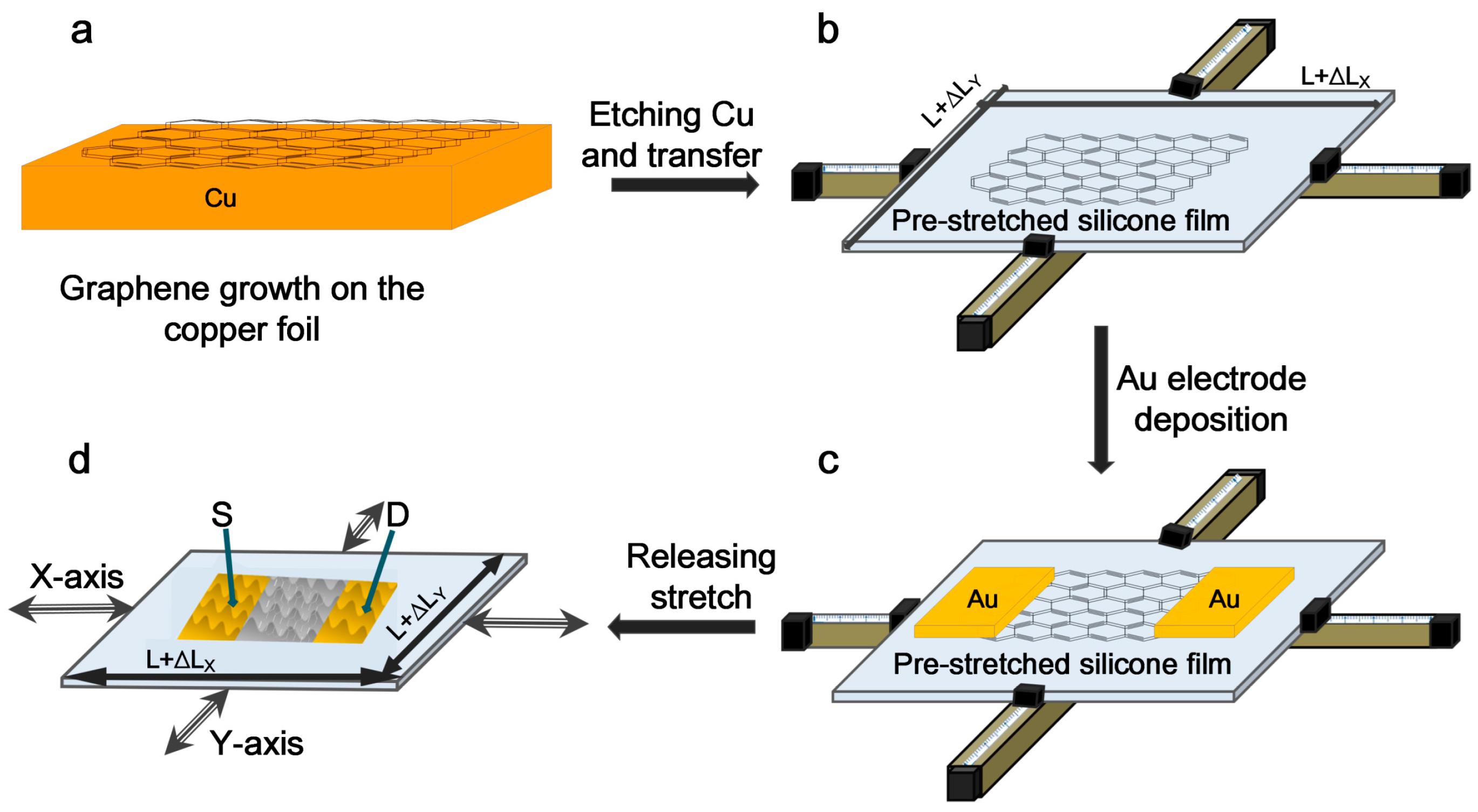
We developed a method to prepare crumpled graphene from normal graphene using a pre-stretched silicone thin film, as illustrated in Figure 1. As shown in Figure 1a, a single layer normal graphene was initially synthesized on a Cu film by chemical vapor deposition (CVD). After post processing, such as PMMA coating, etching of the Cu substrate, and cleaning, the graphene layer was transferred on to a pre-stretched silicone film. The initial size of the elastic silicone film was L·L and the pre-stretched size was L + ΔLx = L + ΔLY = 2L (Figure 1b). Subsequently, a gold electrode (50 nm) was deposited as shown in Figure 1c. After the release of the strain on the silicone film, biaxially crumpled graphene was obtained. The cross aluminum profile was used to control the size of the silicone film from L to L+ ΔLX or ΔLY (0 ≤ ΔLX or ΔLY ≤ L) and the crumpled graphene label.

Figure 1.
Schematic process of the preparation of crumpled graphene. (a) Graphene synthesized on a copper foil via thermal CVD; (b) transfer of post processed single layer graphene onto a pre-stretched silicone elastic film; (c) deposition of the Au electrode; (d) release of the silicone film to obtain crumpled graphene.
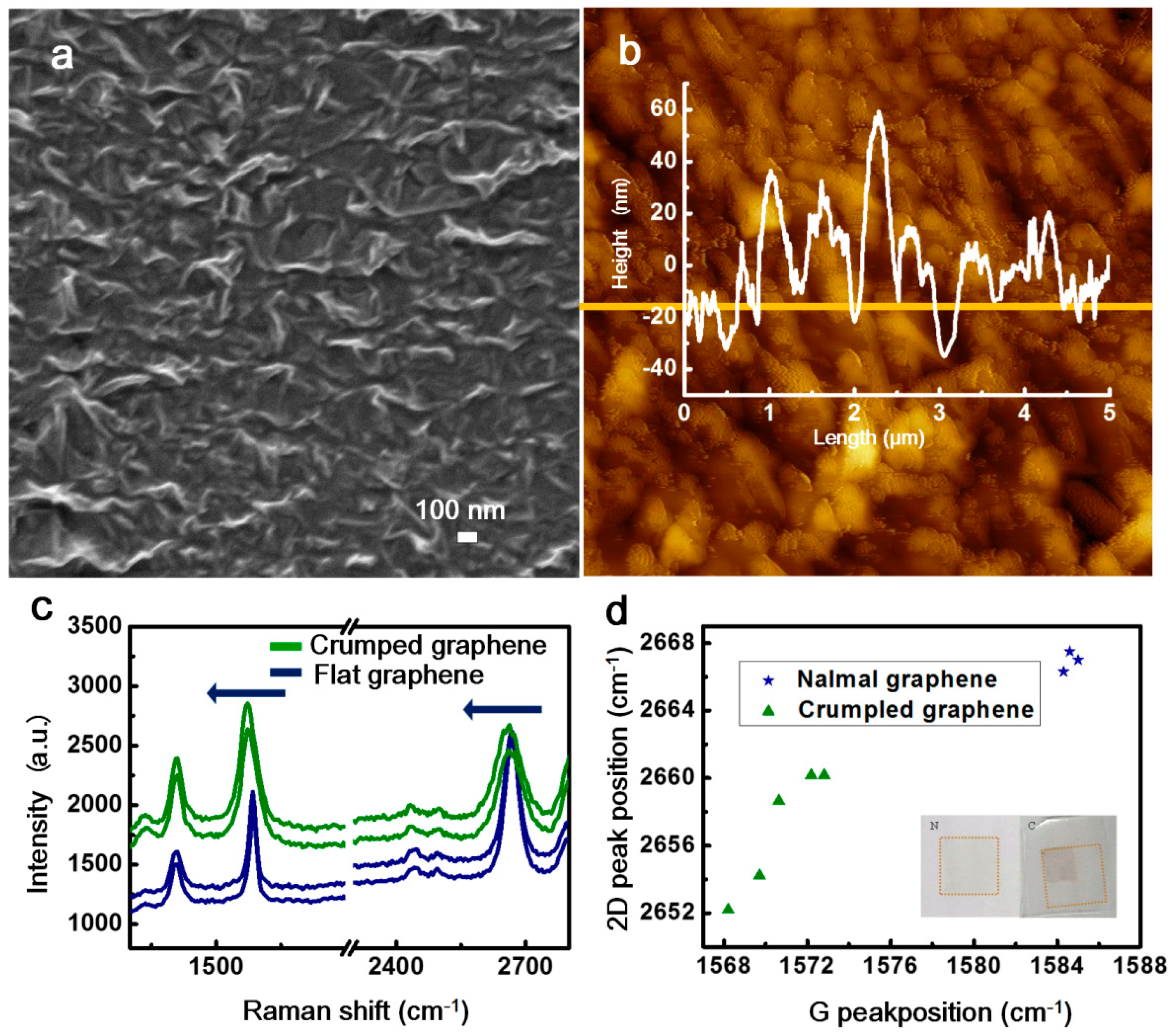
The spontaneous formation of graphene wrinkles during release of the pre-strain is due to the mismatch of the elastic modulus between graphene and the silicone substrate. The surface topology of the as-prepared biaxially crumpled graphene was evaluated using a scanning electron microscope (SEM) and an atomic force microscope (AFM), and the results are shown in Figure 2a,b. The SEM images showed the formation of uniform hundred nanoscale wrinkles because of the crumpling. The AFM data showed the variation in the heights of the wrinkles; the ripple crest is approximately 60 nm, the ripple trough is −40 nm, and the average roughness Ra is 17.5 nm. Raman spectroscopy measurements were conducted to study the structural variations in the crumpled graphene sample, and the results are presented in Figure 2c. Raman spectroscopy can provide a wealth of information on the physical and electronic structures of materials, while being fast and non-destructive. Hence, it is an ideal method to investigate the properties of graphene. Raman spectra in Figure 2c,d show, that there is no significant change in the position of the D peak (disordered structure of graphene) in crumpled graphene when compared to that in normal graphene. This indicates that there is no change in the quality because of the crumpled structure. The G peak (in-plane vibration of sp2 carbon atoms) and the 2D peak (stacking orders) cause shifts in the Raman frequency. This shift in the Raman peak frequency is caused by the distortion of the graphene lattice, which in turn alters the vibrational Raman frequency of the phonons within the lattice [6]. Typically, a compression of the graphene lattice leads to phonon hardening (frequency shift) [7]. The inset in Figure 2d shows the optical microscope (OM) images of the normal and the crumpled graphene samples. After crumpling, the size automatically reduced as indicated by the dark region inside the orange gridline in the inset. Table 1 gives the UV-Visible transmittance of graphene. The transmittance of the normal graphene sample is approximately 97.56%. The crumpled graphene sample exhibited a considerably less transmittance of 85.11% because of the overlapped crumpled structure.
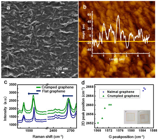
Figure 2.
(a) SEM image of the crumpled graphene; (b) AFM image of the crumpled graphene with the height profile of the cross section shown in the inset; (c) Raman spectra of normal and crumpled graphene samples. The 2D peak shows a frequency red shift; (d) Positions of Raman G and 2D peaks obtained from 5 arbitrary positions on the graphene samples. The inset shows the OM image of the normal and the crumpled graphene samples on the silicone film. The orange gridlines indicate the original size of the graphene sample, and the dark region inside the gridline of crumpled graphene shows the reduction in the area to 1/4 of the initial size.

Table 1.
Transmittance of normal and crumpled graphene (550 nm).
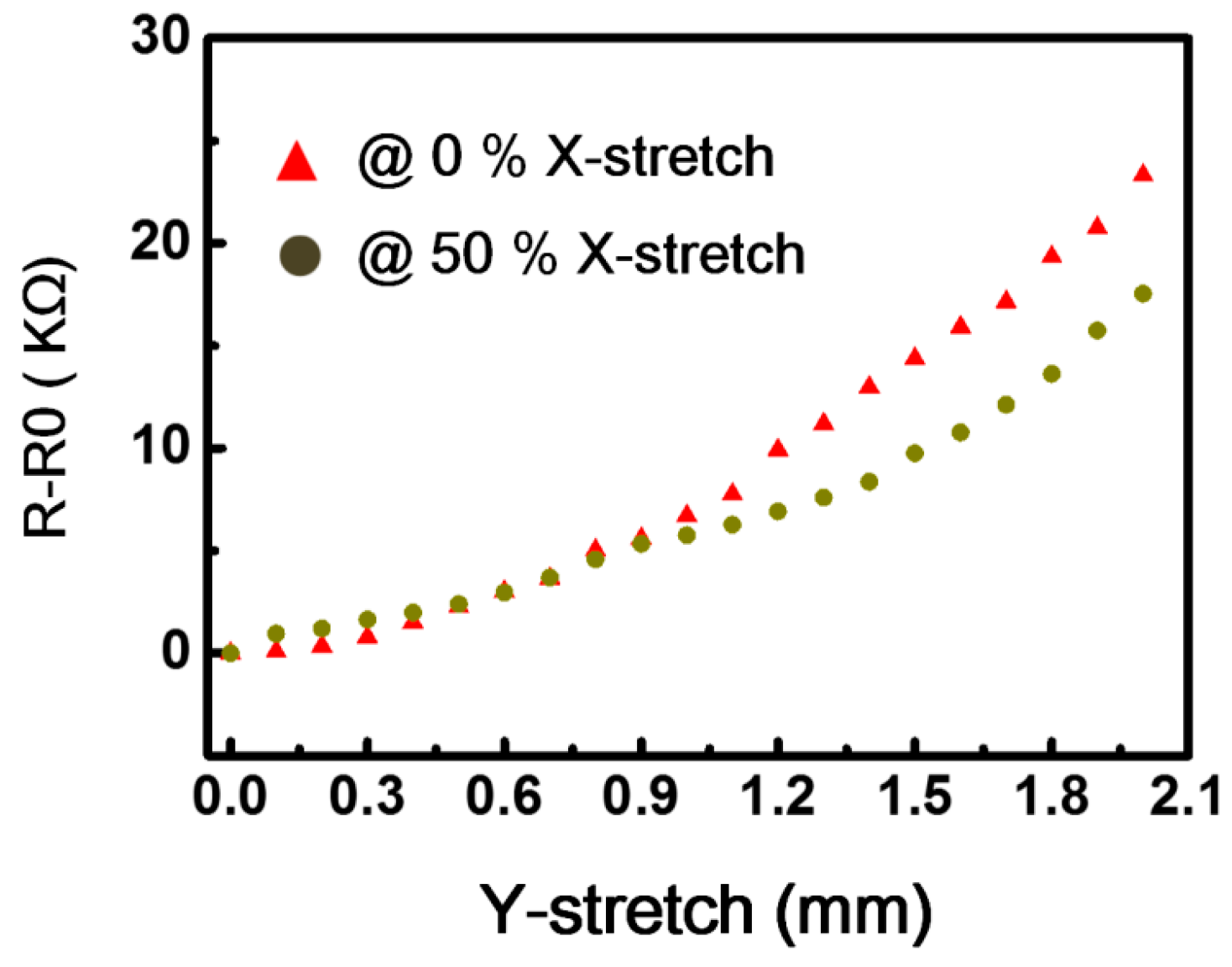
The study of effects of mechanical strain on graphene is very important, particularly for applications such as flexible electronics or strain devices. The electronic structure of graphene can be easily altered by applying a strain. In addition, it is also possible to introduce a band gap into otherwise gapless materials by the application of strain [8]. The variation in the resistance of the crumpled graphene sample due to the applied strain is plotted in Figure 3. To monitor the bi-axial strain, the crumpled graphene was stretched in the X-direction for predefined values like 50 and 100%, and then, a continuous strain was applied in the Y-direction up to 2 mm at increments of 0.1 mm. The change in the resistance due to the biaxial strain was found to be nearly linear (R2 ≥ 0.95). The preliminary results obtained by applying strain in one direction and keeping a fixed strain in the other direction showed a significant change in the resistance, up to 20 kΩ.
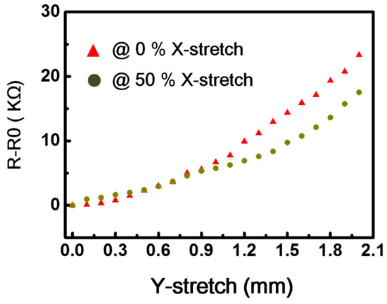
Figure 3.
Variation in the resistance of the crumpled graphene strain sensor under different strains in the Y direction for a fixed X-stretch. To monitor the bi-axial strain, the crumpled graphene was stretched in the X direction for predefined values like 50% and 100%, and then, a continuous strain was applied in the Y-direction up to 2 mm at increments of 0.1 mm.
3. Conclusions
In summary, we fabricated crumpled graphene from normal graphene using a pre-stretched silicone thin film, characterized the changes in the morphology and the structure, and then evaluated the effect of applied strain in two directions. The preliminary results for applied strain in one direction and a fixed strain in the other direction showed a significant change in the resistance, and the change in the resistance was almost linear. We demonstrated that the resistance of graphene depends strongly on the applied tensile strain. The high strain sensitivity of the crumpled graphene sheets suggests its significant potential for applications in strain gauge devices. Additional experiments for studying the applicability of the crumpled graphene sheets in flexible electronics is currently in progress.
Acknowledgments
This work was supported by the National Research Foundation of Korea (NRF) grant funded by the Korea government (MEST) (NRF-2017R1A2B3011222).
Conflicts of Interest
The founding sponsors had no role in the design of the study; in the collection, analyses, or interpretation of data; in the writing of the manuscript, and in the decision to publish the results.
References
- Geim, A.K.; Novoselov, K.S. The rise of graphene. Nat. Mater. 2007, 6, 183–191. [Google Scholar] [CrossRef] [PubMed]
- Lee, C.; Wei, X.; Kysar, J.W.; Hone, J. Measurement of the elastic properties and intrinsic strength of monolayer graphene. Science 2008, 321, 385–388. [Google Scholar] [CrossRef]
- Bae, S.-H.; Lee, Y.; Sharma, B.K.; Lee, H.-J.; Kim, J.-H.; Ahn, J.-H. Graphene-based transparent strain sensor. Carbon 2013, 51, 236–242. [Google Scholar] [CrossRef]
- Wang, Y.; Yang, R.; Shi, Z.; Zhang, L.; Shi, D.; Wang, E.; Zhang, G. Super-elastic graphene ripples for flexible strain sensors. ACS Nano 2011, 5, 3645–3650. [Google Scholar] [CrossRef]
- Fu, X.-W.; Liao, Z.-M.; Zhou, J.-X.; Zhou, Y.-B.; Wu, H.-C.; Zhang, R.; Jing, G.; Xu, J.; Wu, X.; Guo, W. Strain dependent resistance in chemical vapor deposition grown graphene. Appl. Phys. Lett. 2011, 99, 213107. [Google Scholar] [CrossRef]
- Ferrari, A.C. Raman spectroscopy of graphene and graphite: Disorder, electron–phonon coupling, doping and nonadiabatic effects. Solid State Commun. 2007, 143, 47–57. [Google Scholar] [CrossRef]
- Bissett, M.A.; Izumida, W.; Saito, R.; Ago, H. Effect of domain boundaries on the Raman spectra of mechanically strained graphene. ACS Nano 2012, 6, 10229–10238. [Google Scholar] [CrossRef] [PubMed]
- Bissett, M.A.; Tsuji, M.; Ago, H. Strain engineering the properties of graphene and other two-dimensional crystals. Phys. Chem. Chem. Phys. 2014, 16, 11124–11138. [Google Scholar] [CrossRef] [PubMed]
Publisher’s Note: MDPI stays neutral with regard to jurisdictional claims in published maps and institutional affiliations. |
© 2017 by the authors. Licensee MDPI, Basel, Switzerland. This article is an open access article distributed under the terms and conditions of the Creative Commons Attribution (CC BY) license (https://creativecommons.org/licenses/by/4.0/).