Abstract
Gallium oxide nanowires (NWs) were synthetized using a vapor-liquid-solid route via carbothermal reduction. These NWs were characterized using XRD, SEM and TEM as well as photoluminescence spectroscopy, confirming their crystalline nature. Gas sensors, based on individual NWs, deposited on suspended microhotplates, were tested towards several gases of interest at different temperatures. The sensing towards relative humidity provided the best results, with responses up to 20% at room temperature (~25 °C).
1. Introduction
Chemoresistive gas sensors based on metal oxide nanostructures exhibit sensitivities up to parts per billions (ppb) towards different gases [1]. The high surface to volume ratio exhibited in nanostructured materials, and especially in the nanowire (NW) morphology, is a very interesting property in the field of gas sensing. At low temperatures, the adsorption and desorption steady-state of chemical species present in the ambient occurs mostly in the surface, inducing charge transfer and conductance changes in the sensor material. So, the use of NWs instead of thin films as main element of a gas sensor might enhance the sensitivity and selectivity of the final device. The metal oxide studied here is, the monoclinic β-Ga2O3 is a wide band gap material, chemically and thermally stable, well-known for its sensing properties at high temperatures [2,3,4]. This work focuses in the synthesis, physical and optical characterization of β-Ga2O3 NWs followed by the fabrication and characterization of single NW-based gas sensors.
2. Materials and Methods
Using a CVD quartz tube furnace connected to a gas injection system, the Ga2O3 NWs were synthetized via vapor-liquid-solid (VLS) mechanism, first reported by Wagner et al [5]. To lower the evaporating temperature of the precursor material, pure gallium (III) oxide (99.99%) nanopowder, was mixed with graphite powder in a 2:3 weight proportion in an agate mortar for 20 min, to promote a carbothermal reduction during the VLS process. In each experiment 0.25 g of precursor material was used. The substrates were square pieces of Si, with a 0.5 µm-thick SiO2 layer. These substrates were Au sputter-covered for 20 s, giving rise to a thin and discontinuous Au layer. The first step in the VLS mechanism is to evaporate the precursor material, up to 950 °C, and transport it to the substrates, kept at temperatures ranging 800 to 950 °C. The gaseous precursor species interact with the gold particles and recrystallize as NWs with a diameter determined by the initial droplet size. The system was kept at atmospheric pressure during the whole experiment under a flow of 100 mL/min of argon gas with a 5 N purity quality.
The Ga2O3 NWs were structurally investigated by Scanning (SEM) and Transmission Electron Microscopy (TEM) and Grazing Incidence X-Ray Diffraction (GIXRD). Photoluminescence (PL) has been used to further investigate the NWs.
For the fabrication of gas nanosensors, the grown Ga2O3 NWs were transferred to microhotplates with embedded heater and pre-patterned electrodes and the NWs were electrically contacted using a using Focused Electron Beam Induced Deposition (FEBID), following a method explained in detail elsewhere [6]. Gas sensing measurements were performed with a self-constructed stainless-steel gas chamber, of 8.6 mL volume, connected to a self-made gas injection system with 4 Bronkhorst Mass-Flow Controllers. Constant flow of 200 mL/min was kept for the gas measurements. A Keithley 2602A dual Source Measure Unit allowed to control simultaneously the sensor’s resistance and the voltage for heating the microhotplate, using a home-developed Labview software.
3. Results
3.1. Physical Characterization
In our experiments, NWs growth occurs at two different distances from the evaporating source: 2 and 30 cm. In each of them a gold tip at the end of the NWs can be identified, confirming the VLS mechanism. Some nanoplateaux have also been formed, as seen in Figure 1 [7]. The lengths of the NWs ranged 1 to 20 μm of length, while diameters lied between 10 and 50 nm. The NWs grown at different source distances showed different morphological features related to their structural and optical properties, which are discussed later.
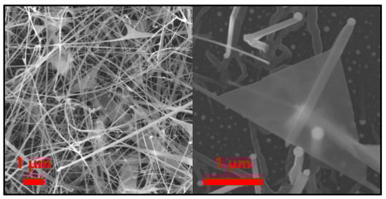
Figure 1.
Gallium Oxide nanowires grown at 30 cm from evaporating source (left) and a detail of a nanoplateaux (right).
3.2. Structural Characterization
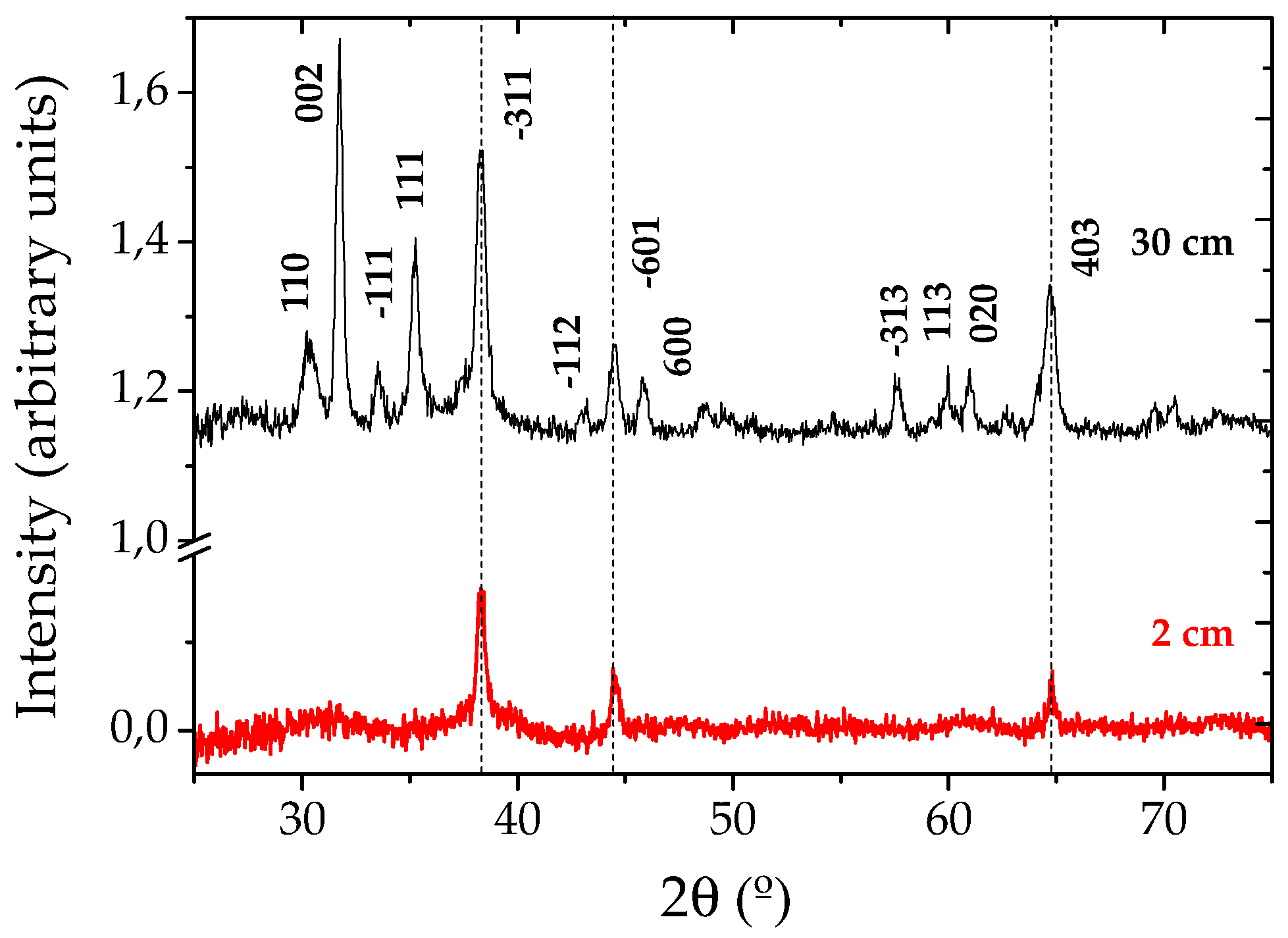
GIXRD measurements were performed at small angle (θ = 0.5°) to increase the interaction volume of the thin Ga2O3 grown NW layer with the incident X-rays. Figure 2 shows two spectra corresponding to the samples grown at 2 and 30 cm from the evaporating source. These spectra perfectly match the standard pattern of monoclinic β-Ga2O3 (JCPDS card 43-1012), with lattice parameters a = 1.2227 nm, b = 0.30389 nm, c = 0.58079 nm, α = γ = 90° and β = 103.82°, in agreement with similar works [8,9,10]. Some additional peaks can be observed, corresponding to the gold catalyst.
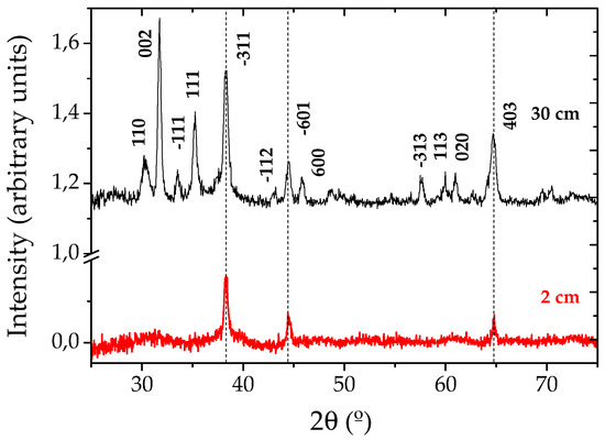
Figure 2.
X-ray diffraction spectra obtained from gallium oxide nanowires grown at 2 and 30 cm from the evaporating source.
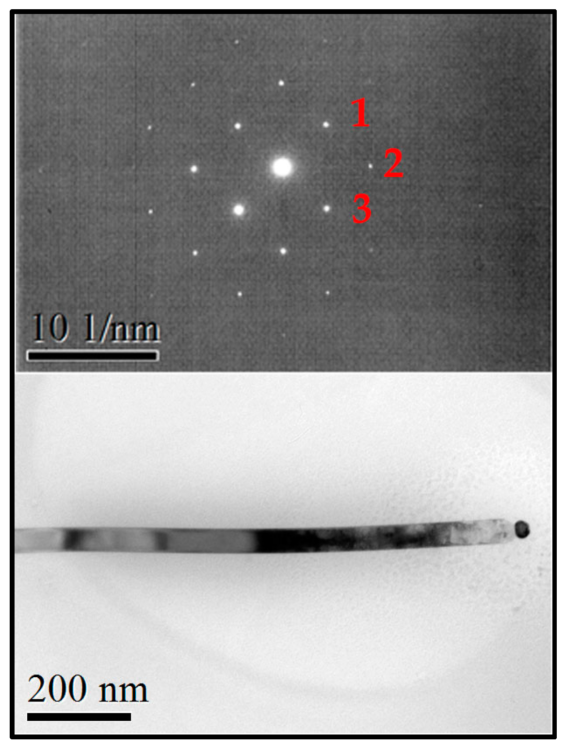
High resolution transmission electron microscopy (HRTEM) analysis of the NWs grown at 30 cm from the evaporating source confirms the monocrystallinity of the Ga2O3 NWs, which grew predominately along the planes, as showed in Figure 3. Herein spots labeled as 1, 2 and 3 correspond to , and indexes respectively and the diffraction pattern is in agreement with the [201] zone axis of monoclínic β-Ga2O3 planes of the crystalline structure.

Figure 3.
Gallium Oxide nanowire (down) and its selected area electron diffraction with spots labeled as 1, 2 and 3 corresponding to , and respectively (up).
3.3. Photoluminiscence Characterization
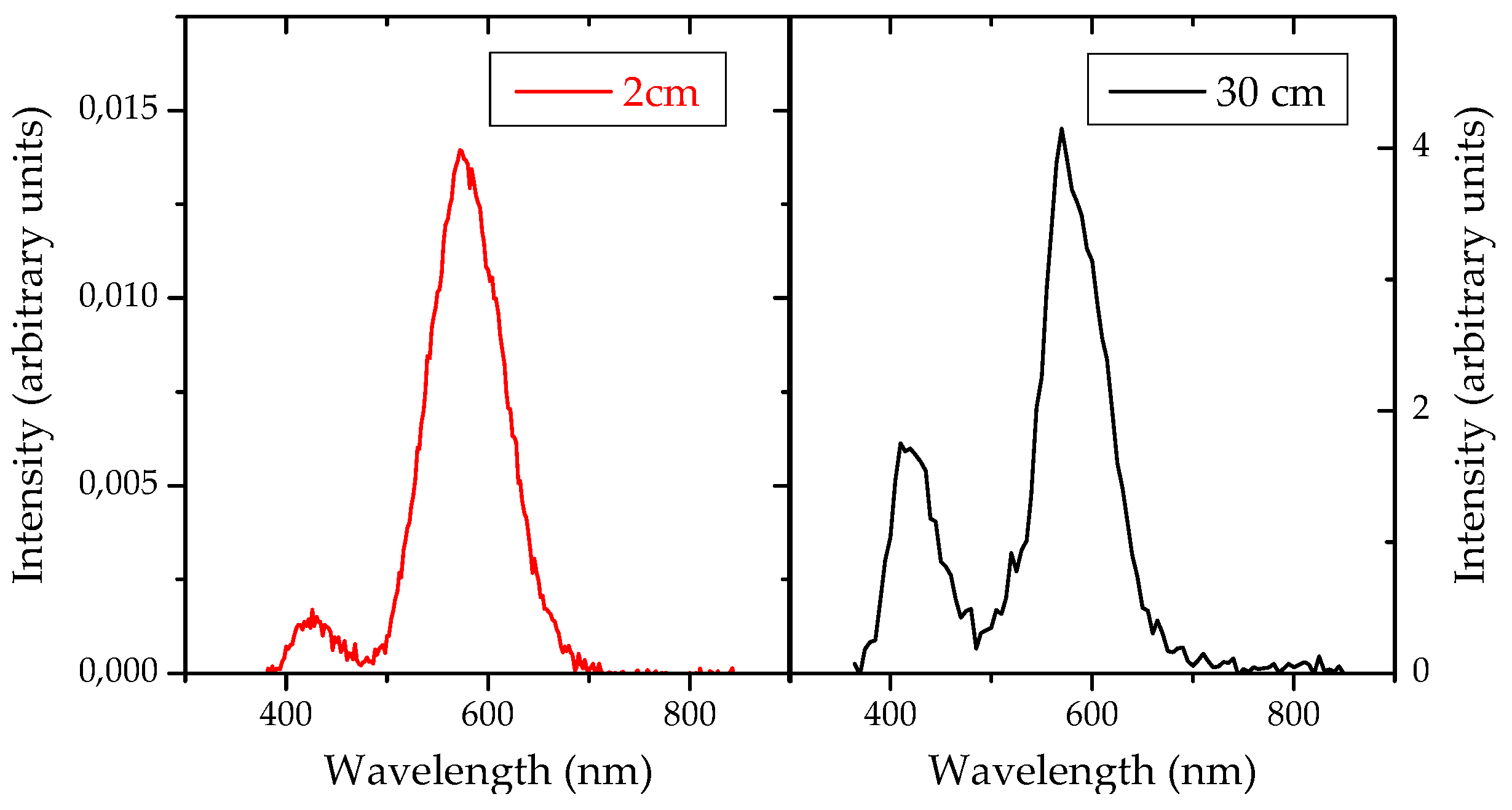
In each spectrum of the two samples with NWs, two different bands can be observed. A strongest one, centered at about 580 nm (yellow) with quite uniform intensity along the whole sample’s surface. And a weaker band, centered at about 430 nm (blue) that appears only in the areas with a high NW density. In both cases showing Gaussian fitting curves, whose width is compatible with other reported experiments [6], where these bands have been assigned to exciton recombination at defects sites, such as oxygen vacancies or Ga-O vacancies. The sample at 30 cm from the precursor source exhibits a stronger overall PL intensity, and a higher intensity of the blue component, that becomes comparable to the yellow one [8,9,10]. This is shown in Figure 4.

Figure 4.
Photoluminescence spectra obtained from gallium oxide nanowires grown at 2 and 30 cm of the evaporating source.
3.4. Gas Response of Single NW-Based Sensor
The resistance evolution of the contacted single Ga2O3 NWs were studied between room temperature (~25 °C) and 250 °C towards different concentrations of oxygen (O2), carbon monoxide (CO), nitrogen dioxide (NO2), relative humidity (RH) and ethanol (EtOH), all diluted in dry synthetic air. In this work we only focused on the response towards relative humidity and oxygen, because their effect can be clearly monitored at this relatively low temperatures, as Ga2O3 usually is operated at temperatures above of 500 °C [11]. In the presence of oxygen, the response traces show an apparent decrease in the resistance. The highest and fastest responses were measured at 250 and 150 °C, respectively, and are presented in Figure 5. On the other hand, the response to relative humidity is considerably high, even at room temperature, with changes up to 20%, with response times below 30 min and recovery times of 1 h, approximately.
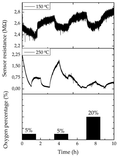
Figure 5.
Resistance evolution of a single gallium oxide nanowire-based sensor towards different pulses of oxygen in a synthetic air ambient at 150 and 250 °C.
4. Conclusions
In this work, gallium oxide NWs were synthetized via vapor-liquid-solid mechanism and their crystalline nature was demonstrated using different techniques. Gas sensors, based on individual NWs, deposited on suspended microhotplates, were fabricated and tested towards several gases of interest at different temperatures. The best sensor response was provided towards relative humidity, reaching values up to 20% at room temperature, and towards oxygen with values up to 8 to 90% at 150 and 250 °C, respectively.
Acknowledgments
The research leading to these results has received funding from the European Research Council under the European Union’s Seventh Framework Program (FP/2007-2013)/ERC Grant Agreement n. 336917 and from the Spanish Ministry of Economy and Competitivness, through projects TEC2013-48147-C6-1-R (AEI/FEDER, EU), TEC2014-62144-EXP and TEC2016-76898-C6-2-R (AEI/FEDER, EU).
Conflicts of Interest
The authors declare no conflict of interest.
References
- Dan, Y.; Evoy, S.; Johnson, A.T. Chemical Gas Sensors Based on Nanowires; Nanowire Research Progress; Nova Science: Hauppauge, NY, USA, 2008; Chapter 3. [Google Scholar]
- Park, S.H.; Kim, S.H.; Park, S.Y.; Lee, C. Synthesis and CO gas sensing properties of surface nitridated Ga2O3 nanowires. RSC Adv. 2014, 4, 63402–63407. [Google Scholar] [CrossRef]
- Juan, Y.M.; Chang, S.J.; Hsueh, H.T.; Wang, S.H.; Weng, W.Y.; Cheng, T.C.; Wud, C.L. Effects of humidity and ultraviolet characteristics on b-Ga2O3 nanowire sensor. RSC Adv. 2015, 5, 84776–84781. [Google Scholar] [CrossRef]
- Liu, Z.; Yamazaki, T.; Shen, Y.; Kikuta, T.; Nakatani, N.; Li, Y. O2 and CO sensing of Ga2O3 multiple nanowire gas sensor. Sens. Actuators B Chem. 2008, 129, 666–670. [Google Scholar] [CrossRef]
- Wagner, R.S.; Ellis, W.C. The vapor-liquid-solid mechanism of crystal growthand its application to Silicon. Appl. Phys. Lett. 1965, 233, 1053–1064. [Google Scholar]
- Vilà, A.; Hernández-Ramírez, F.; Rodríguez, J.; Casals, O.; Romano-Rodríguez, A.; Morante, J.R.; Abid, M. Fabrication of metallic contacts to nanometre-sizedmaterials using a focused ion beam (FIB). Mater. Sci. Eng. 2006, 26, 1063–1066. [Google Scholar] [CrossRef]
- Xiang, X.; Cao, C.B.; Zhu, H.S. Synthesis and photoluminescence of gallium oxide ultra-long nanowires and thin nanosheets. J. Cryst. Growth 2005, 279, 122–128. [Google Scholar] [CrossRef]
- Wu, X.C.; Song, W.H.; Huang, W.D.; Pu, M.H.; Zhao, B.; Sun, Y.P.; Du, J.J. Crystalline gallium oxide nanowires: Intensive blue light emitters. Chem. Phys. Lett. 2000, 328, 5–9. [Google Scholar] [CrossRef]
- Cuong, N.D.; Park, Y.W.; Yoon, S.G. Microstructural and electrical properties of Ga2O3 nanowires grown at various temperatures by vapor-liquid-solid technique. Sens. Actuators B 2009, 140, 240–244. [Google Scholar] [CrossRef]
- Kumar, S.; Kumar, V.; Singh, T.; Hahnel, A.; Singh, R. The effect of deposition time on the structural and optical properties of b-Ga2O3 nanowires grown using CVD technique. J. Nanopart. Res. 2014, 16, 2189. [Google Scholar] [CrossRef]
- Schwebel, T.; Fleischer, M.; Meixner, H. A selective, temperature compensated O2 sensor based on Ga2O3 thin films. Sens. Actuators B 2000, 65, 176–180. [Google Scholar] [CrossRef]

Publisher’s Note: MDPI stays neutral with regard to jurisdictional claims in published maps and institutional affiliations. |
© 2017 by the authors. Licensee MDPI, Basel, Switzerland. This article is an open access article distributed under the terms and conditions of the Creative Commons Attribution (CC BY) license (https://creativecommons.org/licenses/by/4.0/).