Abstract
New chemical sensors are developed for suitable applications in biochemistry and biology, especially for the easy measurement of low concentrations of chemical and biological elements in liquid media. Robust devices, able to detect a small charge variation, can be associated with nanomaterials on the active surface of the sensor. Sensors based on microelectronic technologies and having high sensitivities due to their specific Dual Gate structure are shown. We demonstrate that, under optimum polarization conditions, the sensor exhibits a high sensitivity for pH variations. The integration of several types of nanomaterials on the active surface of the microsensors is also demonstrated and validated for further biological detections.
1. Introduction
Electrochemical sensors have many advantages such as simple use, accuracy, compatibility with the standards of microtechnology and the possibility of integration of various nanomaterials on their active surfaces. Several types of field effect transistor structures exist for chemical detection applications but, however, they suffer from a limited sensitivity [1,2]. In respect to the already existing technologies, the dual gate transistor has many advantages such as robustness, low power consumption and high sensitivity to charge detection due to capacitive amplification [3,4]. In this work, we developed and optimized dual gate transistors, fully compatible with CMOS technologies and high temperature deposition processes necessary for the functionalization of the active surface of the sensors with nanomaterials.
The functionalization of the active surface of the sensor for a selective detection is a key requirement for biosensing applications. For this reason, we aimed to integrate nanomaterials on the active surface of the sensors. In addition, using nanomaterials allows increasing the active specific surface area which is expected to enhance the overall sensitivity of the device. For this purpose, two types of nanomaterials have been studied and grown on the active layer.
2. Materials and Methods
Dual Gate Field Effect Transistors have shown interesting properties, especially for charge detection. Their structure is comparable to the one of a classical field effect transistor, but they can be polarized with two gate voltages where one of them is the bottom gate, usually fabricated at the beginning of the process. The second gate is fabricated on the surface of the device or can be linked with liquid media as in ISFET structures. In this particular configuration, electrical charges linked at the surface of the device leads to a modification of the current–voltage transfer characteristic. This effect can be enhanced by the capacitance ratio between top and bottom gate insulators. The sensitivity is then clearly enhanced. Based on field effect transistor theory as well as Dual Gate FET theory, the variation of the threshold voltage is given by [3]:
With Vth,bottom and VGTop constant, charges located on the surface create a variation of Vth,Top, that is enhanced by the capacitance ratio and the measured variation is then given by:
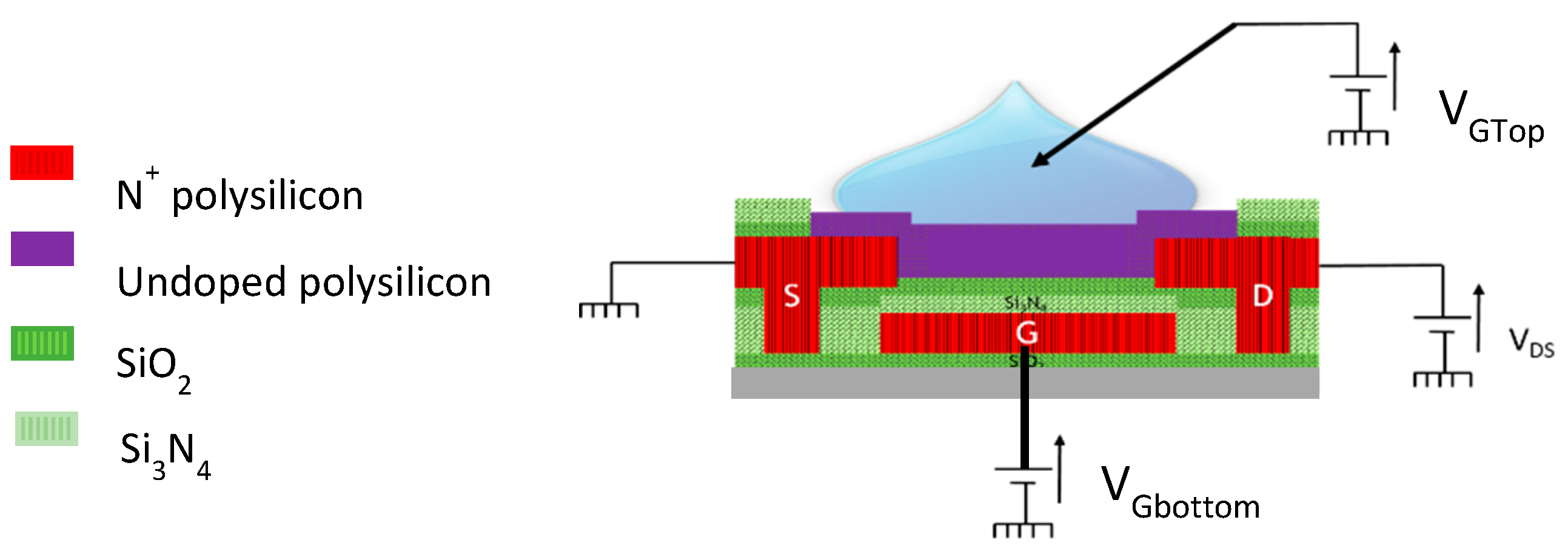
We have developped Dual Gate Field Effect Transistors by using a technology based on classical thin film transistors with polysilicon active layer as shown Figure 1. Source, drain and gate contacts are made with highly N doped polycrystalline silicon deposited by LPCVD. The active layer of the device is made of undoped polysilicon. Its thickness is 100 nm. This process is fully compatible with high temperature treatments for further integration of nanomaterials and surface functionnalization of the top active surface. The gate insulator characteristics have been optimized in order to decrease the threshold voltage while keeping a very low leakage current. With a combinaison of 50 nm thick silicon nitride and 50 nm thick silicon dioxide, we obtain a bottom gate field effect transistor with a threshold voltage of 10 V and a field effect mobility of 10 cm2/V·s.

Figure 1.
Dual Gate Field Effect Transistor – structure and measurement setup.
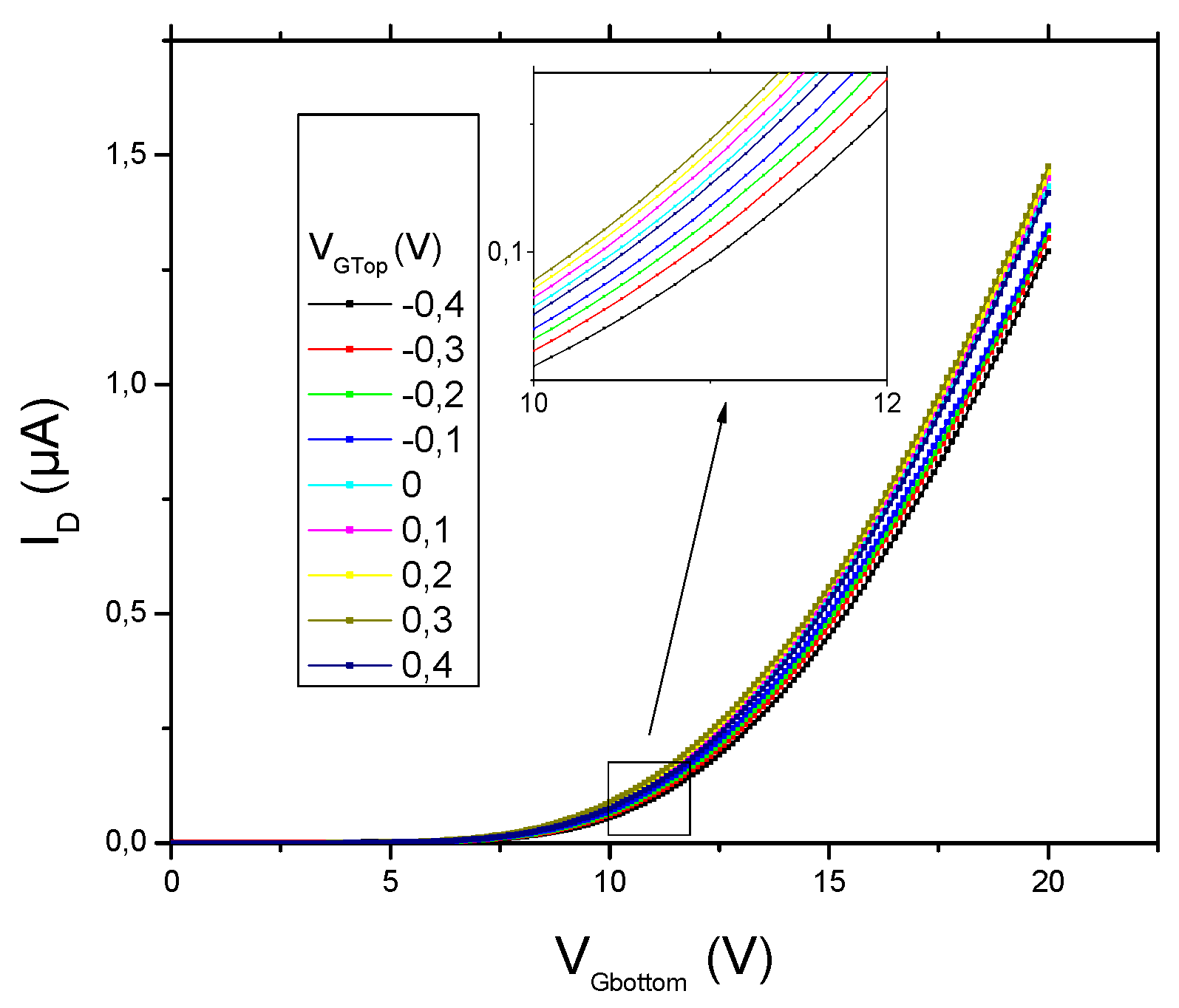
Electrical contacts are insulated from the liquid. The active layer made of silicon is covered with a very thin native oxide. In the dual gate mode, 6 μL of different liquids are dropped on the active area and polarized for Dual Gate operation. As expected, the top gate voltage influences the transfer characteristic as shown Figure 2.
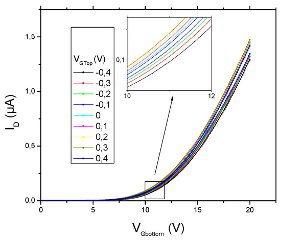
Figure 2.
Influence of the top gate voltage on the transfer characteristics.
3. Results
3.1. Sensitivity to pH
In the case of pH, the variation of the threshold voltage is limited by Nernst theory to 59 mV/pH [1]. In the case of Dual Gate FET, the measured sensitivity versus pH can be expressed by:
The electrical characteristics of the devices are studied as a function of both gate polarizations. The charge detection measurements are carried out, using different pH solutions, with various conditions of the dual gate operation mode. The intrinsic capacitive amplification depends on the native oxide thickness which can be estimated. The theoretical amplification with this structure can reach 15.
Transfer characteristics are presented in Figure 3 for three pH values. In this case, the bottom gate voltage is varied and the top gate voltage is fixed to 0 V. As expected, a decrease in pH results in a shift of the transfer characteristic leading to a decrease in the threshold voltage (Figure 3a).
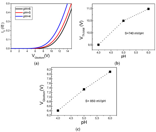
Figure 3.
(a) Transfer characteristics with different pH values; (b,c) calibration curve and sensitivities.
High sensitivities can be measured by selecting a specific bottom gate value. The sensitivity can also be determined with the threshold voltage shift, or even for a given ID value at lower bottom gate voltage. Sensitivities of 740 mV/pH and 850 mV/pH have been recorded under these two conditions (Figure 3b,c) which demonstrate the ability of such devices to operate as highly sensitive charge sensors, suitable for biochemical detections.
3.2. Integration of Nanomaterials
The integration of nanomaterials on the surface of the device has two major interests. It allows first to increase the active surface in contact with the ambient medium. This effect can be beneficial as it may allow enhancing the sensitivity of the device which is mandatory for the detection of species with very low concentrations or for the detection of small variations in a given medium. Moreover, the choice of a suitable surface material is decisive for an easier functionalization necessary for a selective detection. In this context, carbon or silicon are ideal candidates as their functionalizations have been previously studied.
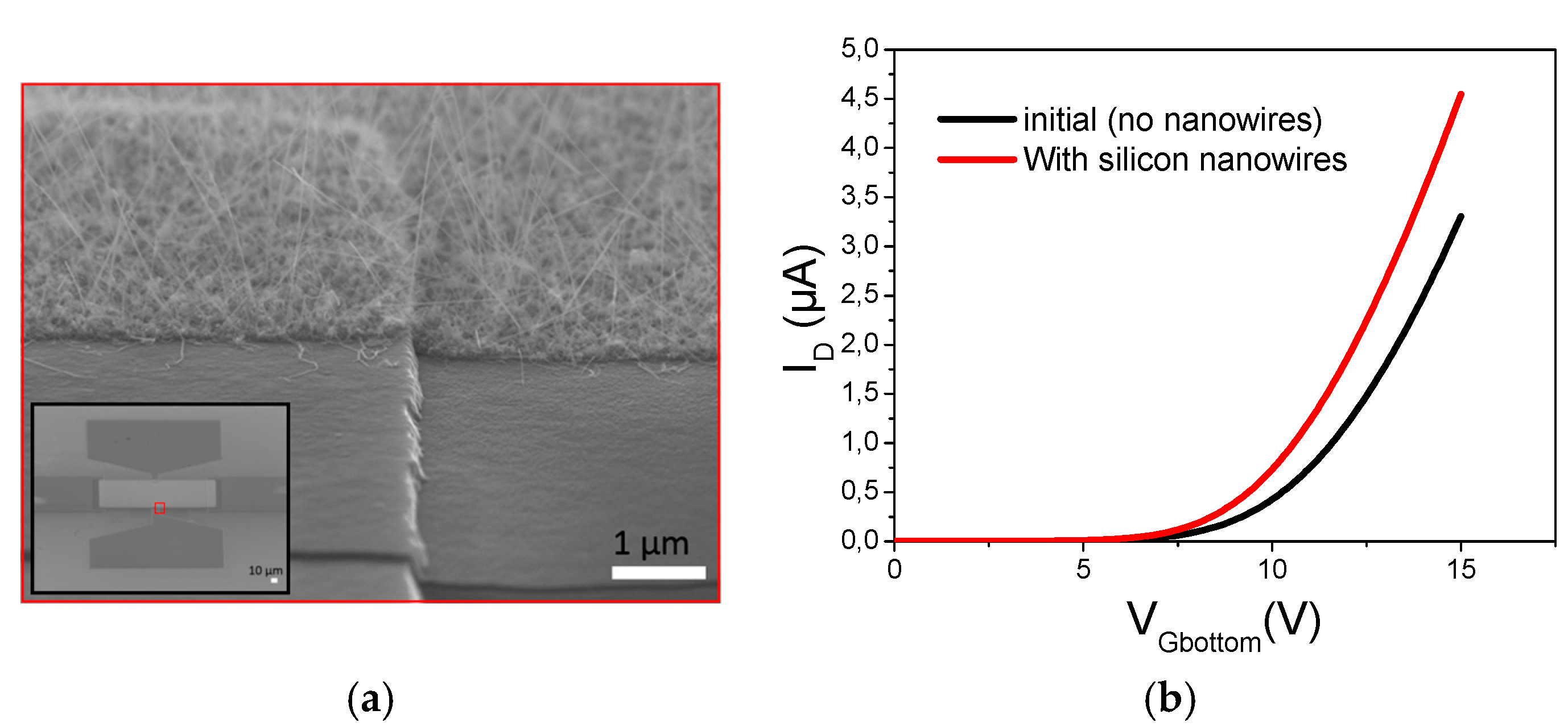
In this work, two types of nanomaterials have been considered and grown on the active layer of the devices: (i) silicon nanowires; and (ii) nanoporous carbon [5]. The first objective was to develop a nanomaterial growth process compatible with the specific technology and materials employed to manufacture the transistors. The growth of nanostructures on the active surface is expected to impact the electrical characteristics of the devices, but could in parallel greatly enhance their sensitivity. For this purpose, silicon nanowires were first considered. In Figure 4 is presented a typical SEM image of the active surface of the device after integration of the silicon nanowires using a VLS (Vapor Liquid Solid) process [6]. The electrical characteristics of the device presented in Figure 4b validate the compatibility of silicon nanowires with FET structure.
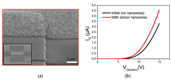
Figure 4.
Integration of silicon nanowires on the active layer of the device: (a) SEM image showing the forest of silicon nanowires covering the active later and (b) I/V characteristics of the device before and after integration of the nanowires.
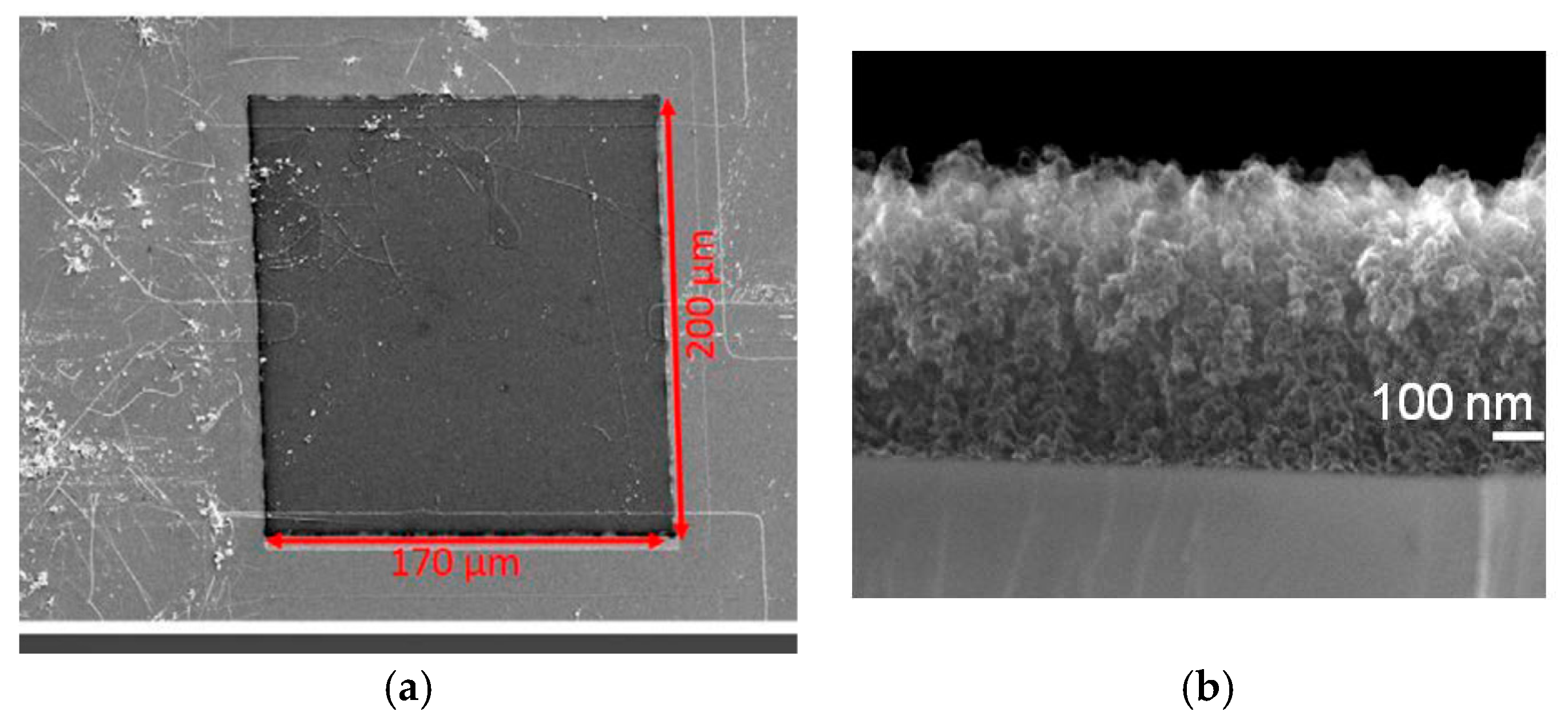
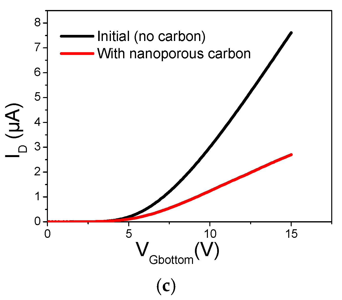
The second material we considered is nanoporous carbon. It was grown using an original approach involving the deposition of copper/carbon nanocomposite film followed by selective etching of copper in nitric acid allowing obtaining a nanoporous skeleton of carbon. As shown in Figure 5a,b, this material was successfully synthesized over the active layer made of silicon. The transistor was neither destroyed during the deposition of the copper/carbon film nor during the selective etching of copper using nitric acid. As shown Figure 5c, the transfer characteristic of the device is modified after the nanocarbon integration but maintains, however, a reasonable electrical characteristic sufficient for sensing applications.

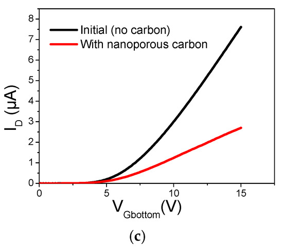
Figure 5.
Nanoporous carbon on active layer: (a,b) SEM images; (c) effect on transfer characteristics.
4. Conclusion
We have developed a technological process for the manufacturing of Dual Gate Field Effect Transistor, compatible with high temperature treatments and measurements in liquid media. As shown by the theory, the sensitivity of charge detection is enhanced by the ratio of gates insulator capacitances. First results for pH measurement led to a sensitivity higher than 800 mV/pH, showing the interest of using such devices for biochemical applications. Furthermore, the integration of two different nanomaterials has been demonstrated without degradation of the devices characteristics. The combination of these two technologies (DG-FET and nanomaterials) is expected to pave the way for the development of highly sensitive biochemical sensors.
Acknowledgments
The authors wish to thanks Olivier de Sagazan, Christophe Lebreton and Brice Le Borgne for technological support and clean room facilities and the ANR for financial support. This publication is also supported by the European Union through the European Regional Development Fund (ERDF), and by the french region of Brittany and Pays de la Loire, le Ministère de l’enseignement supérieur et de la recherche, Rennes Métropole, et le Conseil Départemental 35, through the CPER Projects TechnoCap and SOPHIE/STIC & Ondes.
Conflicts of Interest
The authors declare no conflict of interest.
References
- Bergveld, P. Thirty years of ISFETOLOGY: What happened in the past 30 years and what may happen in the next 30 years. Sens. Actuators B Chem. 2003, 88, 1–20. [Google Scholar] [CrossRef]
- Van Hal, R.E.G.; Eijkel, J.C.T.; Bergveld, P. A novel description of ISFET sensitivity with the buffer capacity and double-layer capacitance as key parameters. Sens. Actuators B Chem. 1995, 24, 201–205. [Google Scholar] [CrossRef]
- Spijkman, M.J.; Brondijk, J.J.; Geuns, T.C.; Smits, E.C.; Cramer, T.; Zerbetto, F.; Stoliar, P.; Biscarini, F.; Blom, P.W.; de Leeuw, D.M. Dual-gate organic field-effect transistors as potentiometric sensors in aqueous solution. Adv. Funct. Mater. 2010, 20, 898–905. [Google Scholar] [CrossRef]
- Jang, H.-J.; Cho, W.-J. Performance Enhancement of Capacitive-Coupling Dual-Gate Ion-Sensitive Field-Effect Transistor in Ultra-Thin-Body. Sci Rep. 2014, 4. [Google Scholar] [CrossRef] [PubMed]
- Donero, L.; Bouts, N.; El Mel, A.A.; Le Borgne, B.; Gautron, E.; Le Brizoual, L.; Le Bihan, F.; Tessier, P.Y. Effect of temperature on the synthesis of nanoporous carbon from copper/carbon thin films to nanoporous carbon for sensing applications. Thin Solid Films 2017, 630, 59–65. [Google Scholar] [CrossRef]
- Demami, F.; Ni, L.; Rogel, R.; Salaun, A.-C.; Pichon, L. Silicon nanowires based resistors as gas sensors. Sens. Actuators B Chem. 2011, 170, 158. [Google Scholar] [CrossRef]

Publisher’s Note: MDPI stays neutral with regard to jurisdictional claims in published maps and institutional affiliations. |
© 2017 by the authors. Licensee MDPI, Basel, Switzerland. This article is an open access article distributed under the terms and conditions of the Creative Commons Attribution (CC BY) license (https://creativecommons.org/licenses/by/4.0/).