Abstract
The realization of 30 µm-deep trench isolation in a linear array of butt-coupled 3D CMOS silicon photodetectors is investigated by implementing the formation of a shallow n+-p junction and SiO2-liner over the trench sidewalls as well as the SU-8 filling trenches for passivation. The dependency of the dark I-V curve on the trench isolation scheme is analyzed by monitoring the dynamic dark I-V measurements of four samples including the schemes of single-trench isolation with different widths and the scheme of double-trench isolation. The highest and the lowest dark currents are measured in the detectors with the widest single-trench isolation and the double-trench isolation, respectively.
1. Introduction
The performance of a photodetector array based on a common p-type silicon substrate is significantly impressed by the crosstalk and the dark current. Therefore, the implementation of qualified passivation and isolation methods is imperatively required to reduce leakage and the dark currents.
The approach of deep trench isolation up to 4 µm deep has been presented for pixel isolation in CMOS image sensor [1]. However, the implementation of deep trench isolation suffers from the dark current enhancement due to the increase of the interfacial defects at the trench sidewalls. In prior works, the metal-oxide-semiconductor (MOS) capacitor deep trench isolation including doped polysilicon filled trenches [2] and the metal-insulator-silicon deep trench isolation [3] in the accumulation mode were integrated into CMOS image sensors.
In this work, the approach of 30 µm-deep trench isolation is used to increase the efficiency of pixel isolation in a 3D butt-coupled photodetector array with a vertically photoactive area as deep as 30 µm [4,5]. Here, the aforementioned methods for passivation and filling trenches could not be used efficiently. Hence, the reduction of the dark current originating from ultra-deep trenches is a very challenging problem. To tackle it, the 3D pn junction deep trenches, which are filled by SU-8 polymer, with two schemes of single-trench isolation and double-trench isolation are studied to realize the lowest dark current value. The proposed method takes advantage of the electrical properties improvement in a p-type silicon substrate and the efficient trench sidewalls treatment by phosphorous diffusion gettering procedure [6], and the low thermal budget process for filling the trenches with SU-8 polymer.
2. Materials and Methods
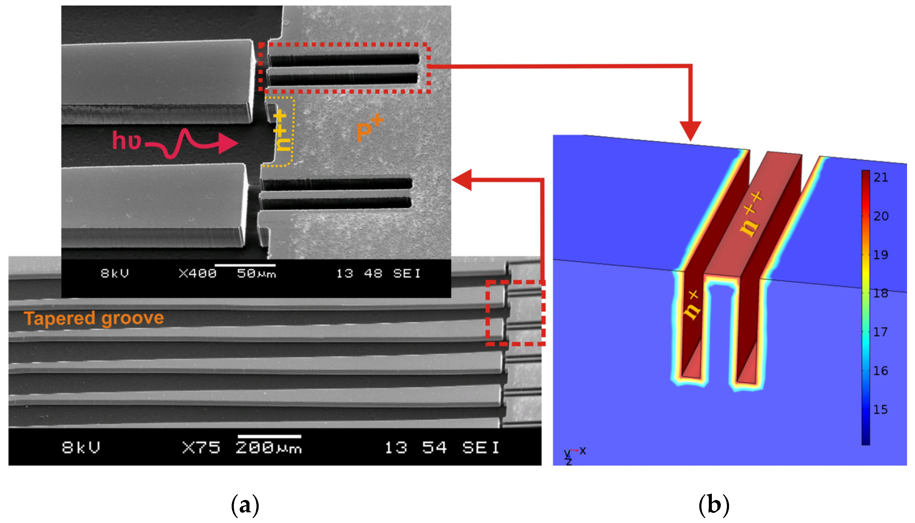
For the fabrication of a 3D butt-coupled photodetector array, the deep reactive ion etching (DRIE) process is applied after the formation of the p+ and n++ high doping level regions, respectively, used for ohmic contacts as shown in Figure 1a. The trench sidewalls are treated by exploiting a POCl3+N2 diffusion to form a shallow n+-p junction with a junction depth of about 300 nm and a surface doping concentration of about 5 × 1020 cm−3. In this step, the surface doping concentration and the junction depth at the trench sidewalls are also adapted to form a vertical photoactive area in the illuminated side for the visible spectral range. The doping profile over the sidewalls is simulated three-dimensionally (3D) by COMSOL Multiphysics. The simulation is carried out by introducing the surface doping concentration and the junction depth, which are measured by secondary ion mass spectrometry (SIMS) on a test wafer. Figure 1b exhibits the simulated doping profile over the double-trench isolation. The measured phosphorous diffusion parameters are presented in Table 1. In the next step, a thin layer of 150 nm SiO2 is thermally grown over the trench sidewalls, which is called SiO2-liner.

Figure 1.
(a) SEM images of 3D butt-coupled detector structure with a tapered fiber couplers platform before the passivation and the formation of electrical interconnections; (b) the simulated doping profiles over double trench isolation by COMSOL Multiphysics.

Table 1.
The measured POCl3+N2 diffusion parameters by SIMS on a test wafer.
The process of SU-8 filling of the trenches was developed to realize a uniform filling of the trenches without formation of voids or air bubbles and to achieve a planarized surface over 150 mm silicon wafer without any additional planarization process like chemical mechanical polishing (CMP) or etch-back processes. The process development was carried out by adjusting the parameters of SU-8 viscosity, spin coat, and lithography. The desired outcome was realized by stacking two polymer layers of SU-8, one layer of SU-8 2002 with a lower viscosity of 7.5cSt and one layer of SU-8 2005 with a higher viscosity of 45cSt.
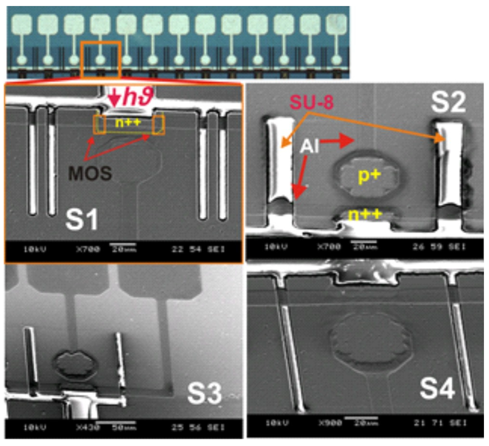
Figure 2 shows the scanning electron microscope (SEM) images of four photodetectors with different trench isolation schemes. Photodetectors with a single-trench isolation scheme with different widths of about 24 µm (S2), 13 µm (S3), and 8 µm (S4) are included in the figure. In the photodetector with the double-trench isolation scheme (S1), the width of the trenches is about 7.5 µm.

Figure 2.
Tilted top-view SEM images of four samples with double-trench isolation and different single-trench isolation widths. (The included optical microscope image shows the linear detector array of the isolation scheme S1).
3. Results and Discussion
The dynamic dark I-V measurement with a delay time of 2 s is carried out by using two needle probes and a Keithley 2400 SourceMeter inside a light-tight box. The dark I-V curves for the four samples are plotted in Figure 3a. The dark I-V curves are highly dependent upon the width of the trench isolation and the schemes of the trench isolation. As represented in Table 2, the dark current values decreased by reducing the width of the single-trench isolation. In addition, the lowest dark current value of 1.14 nA and the highest dark current value of 520 µA at 2 V reverse bias are measured in the photodetectors with the double-trench isolation (S1) and the single-trench isolation with a width of 24 µm (S2), respectively. This observation is attributed to the effect of a local compressive stress induced by the SU-8 polymer on the shallow n+-p junction over the trench sidewalls. The local compressive stress may result in a reduction of the energy bandgap, which is leading to an enhancement of minority carrier concentration and dark current.
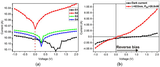
Figure 3.
(a) Semi-logarithmic dark I-V measurements for the four samples; (b) non-illuminated and illuminated I-V curves for sample S1 with double-trench isolation.
Table 2.
The dark current values at 2V reverse bias for the four presented samples.
The semi-logarithmic I-V curves in Figure 3a show clearly a shift of the I-V curve towards the reverse bias voltage, while the dark current level is diminishing in the samples. This observation is attributed to the metal-oxide-semiconductor (MOS) structure located at the n++ region (see Figure 2), and to electrons trapped at the Si-SiO2 interfaces. Electrons accumulate under the applied positive reverse voltage at the Si-SiO2 interfaces. These electrons are related to the capacitors and bias the pn-junction. For higher dark currents, the I-V curves are shifted towards zero applied voltage due to the decreasing contribution of charging and discharging the trapped electrons at Si-SiO2 interface in MOS capacitors to the output current.
For the photodetector with double-trench isolation (S1), the I-V curve is measured under the illumination of He-Ne laser at a wavelength of 633 nm with an incident light power of 28.8 nW. I-V curves of sample S1 are plotted in Figure 3b without and with illumination. Besides, this photodetector demonstrates a photoresponsivity of 0.27 A/W, corresponding to an external quantum efficiency of 54.63%, at 2 V reverse bias.
4. Conclusions
The implementation of ultra-deep trench isolation as deep as 30 µm in a linear butt-coupled 3D CMOS silicon photodetector array was successfully realized by exploiting an efficient passivation method. The passivation method of the deep trenches involved a 300 nm-deep n+-p junction, SiO2-liner, and SU-8 for filling the trenches. The dark I-V curves versus the schemes and the widths of deep trench isolation were analyzed. One can observe that the dark current was reduced by decreasing the single-trench isolation width due to the reduction of compressive stress on the n+-p junction. The scheme of double-trench isolation with a trench width of about 7.5 µm in the presented photodetector resulted in the lowest dark current of 1.14 nA at 2 V reverse bias.
Acknowledgments
The authors would like to thank cleanroom staff in semiconductor technology group of IMOS institute for their technical supports.
Conflicts of Interest
The founding sponsors had no role in the design of the study; in the collection, analyses, or interpretation of data; in the writing of the manuscript, and in the decision to publish the results.
References
- Park, B.J.; Jung, J.; Moon, C.R.; Hwang, S.H.; Lee, Y.W.; Kim, D.W.; Paik, K.H.; Yoo, J.R.; Lee, D.H.; Kim, K. Deep Trench Isolation for Crosstalk Suppression in Active Pixel Sensors with 1.7 µm Pixel Pitch. Jpn. J. Appl. Phys. 2007, 46, 2454. [Google Scholar] [CrossRef]
- Ahmed, N.; Roy, F.; Lu, G.N.; Mamdy, B.; Carrere, J.P.; Tournier, A.; Virollet, N.; Perrot, C.; Rivoire, M.; Seignard, A.; et al. (Eds.) MOS Capacitor Deep Trench Isolation for CMOS image sensors. In Proceedings of the 2014 IEEE International Electron Devices Meeting, San Francisco, CA, USA, 15–17 December 2014. [Google Scholar]
- Kitamura, Y.; Aikawa, H.; Kakehi, K.; Yousyou, T.; Eda, K.; Minami, T.; Uya, S.; Takegawa, Y.; Yamashita, H.; Kohyama, Y.; et al. (Eds.) Suppression of crosstalk by using backside deep trench isolation for 1.12 μm backside illuminated CMOS image sensor. In Proceedings of the 2012 International Electron Devices Meeting, San Francisco, CA, USA, 10–13 December 2012. [Google Scholar]
- Sabri Alirezaei, I.; Vierhaus, J.; Burte, E.P. A 3D-CMOS compatible silicon photo-sensor with a large vertical photosensitive area. Opt. Quantum Electron. 2017, 49, 123. [Google Scholar] [CrossRef]
- SabriAlirezaei, I.; Vierhaus, J.; Burte, E.P. (Eds.) A Butt-Coupled 3D-Bulk Si CMOS Photodetector Array Integrated with a Monolithic U-Groove Array on a Single Chip; Optical Society of America: Washington, DC, USA, 2017. [Google Scholar]
- Lotfi, D.; Hatem, E. Phosphorus diffusion gettering process of multicrystalline silicon using a sacrificial porous silicon layer. Nanoscale Res. Lett. 2012, 7, 424. [Google Scholar] [CrossRef] [PubMed]
Publisher’s Note: MDPI stays neutral with regard to jurisdictional claims in published maps and institutional affiliations. |
© 2017 by the authors. Licensee MDPI, Basel, Switzerland. This article is an open access article distributed under the terms and conditions of the Creative Commons Attribution (CC BY) license (https://creativecommons.org/licenses/by/4.0/).