Abstract
A composite, capillary-driven microfluidic system suitable for transmitted light microscopy of cells (e.g., red and white human blood cells) is fabricated and demonstrated. The microfluidic system consists of a microchannels network fabricated in a photo-patternable adhesive polymer on a quartz substrate, which, by means of adhesive bonding, is then connected to a silicon microfluidic die (for processing of the biological sample) and quartz die (to form the imaging chamber). The entire bonding process makes use of a very low temperature budget (200 °C). In this demonstrator, the silicon die consists of microfluidic channels with transition structures to allow conveyance of fluid utilizing capillary forces from the polymer channels to the silicon channels and back to the polymer channels. Compared to existing devices, this fully integrated platform combines on the same substrate silicon microfluidic capabilities with optical system analysis, representing a portable and versatile lab-on-chip device.
1. Introduction
Capillary-driven systems in the form of paper-based lateral flow assays have been on the market for decades with applications ranging from pregnancy testing to water quality control [1]. More recently, researchers have demonstrated micromachined microfluidic systems, in substrates ranging from silicon [2] to plastic [3], which expand the range of bioassays that can be performed using passive, capillary-driven flow control and pumping techniques. Silicon processing allows for small, accurate, and reproducible features to be fabricated with aspect ratios up to approximately 50:1. However, the optical opacity in the visible spectrum makes this material unsuited for transmitted light microscopy. In this work, a composite microsystem is developed and demonstrated utilizing a quartz glass substrate, a silicon microfluidic chip and quartz glass cover. The components of the microsystem are bonded together utilizing a photo-patternable adhesive layer, which also contains microfluidic channels to transfer fluid to the different components. The device is then tested using diluted human blood and the images of Red Blood Cells (RBCs) are collected. The high quality of the recorded pictures proved the integrity of the transparent substrate, thus validating the feasibility of the integration process.
2. The Silicon-Quartz Opto-Fluidic Platform
The outline of the device is shown in Figure 1a. The 3D schematic (top) highlights the arrangement of the single components on the assembled chip, while the different materials and layers are presented in the cross section (bottom). As clear from the drawings, the fabrication process involves the assembly of three different subdevices. The devices are assembled together using a polymer assisted bonding process. The bonding polymer is lithographically patterned, providing a fluidic connection between the bottom wafer and the top silicon die. The polymer fluidic channels drive the fluid first into the silicon chip, which is deputed to the fluid manipulation. Exploiting the high aspect ratio etch possibilities and the very good control on the channels width, many operations like timing, metering and mixing are indeed possible by proper shaping the fluid circuitry. Once processed, the fluid is transferred back into the polymer and then into the imaging chambers, fabricated by capping the polymer channels with a quartz die. While the functional layers are present on the silicon die and on the polymer layer, the third chip has indeed the only function of protecting the fluid to better control its propagation in the imaging chambers and limit the evaporation phenomena. Once driven into the imaging chambers, the fluid can be properly imaged by means of transmission microscopy or similar techniques.
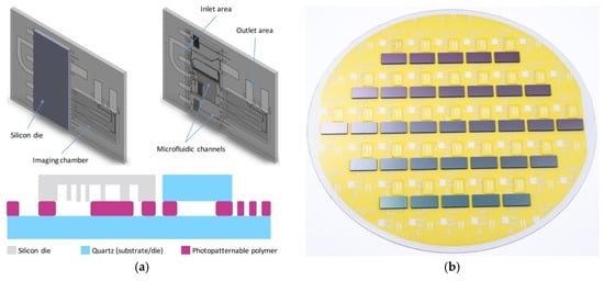
Figure 1.
(a) Device schematics. (Top) 3D view of the main system components. (Bottom) Microchip cross-section view; (b) Image of the 200 mm wafer populated with silicon and quartz dies.
2.1. Device Fabrication Process
The adhesive bonding interface is provided by coating a 200 mm quartz wafer with a photopatternable polymer. A bottom antireflective coating layer is used to provide a correct lithography exposure over the 30 microns thick resist. The microchannels patterned into the polymer provide a fluidic link between the silicon and quartz bonded chips that will be later bonded. Conventional G-Line lithography is used to define a microchannels network on a <100> 200 mm silicon wafer in combination with a silicon Nitride/Oxide hard mask process. The silicon is etched by means of Bosch process into different depth, to provide multiple device functionalities (valves, timing channels). The silicon is finally diced into 1 cm × 1.8 cm dies. In parallel, a bare quartz wafer is also diced in 0.5 cm × 0.8 cm dies. The silicon chip and the photopatternable polymer are shown in Figure 2a,b. The final device assembly happens into an industrial BESI die to wafer bonding tool. After bonding and curing of the adhesive polymer layer, the devices are coated with 3[Methoxy(polyethyleneoxy)propyl]trimethoxysilane using a vapor-phase process to render the surfaces of the adhesive polymer, quartz, and silicon hydrophilic (i.e., suitable for capillary-driven flow).
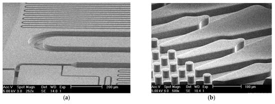
Figure 2.
SEM images of the fabricated chips. (a) The silicon chip: Channels width varies from 10 um to 100 um; (b) The patterned polymer channels.
2.2. The Bonding Process
The final device assembly is performed using a BESI 8800 TC Advanced equipment. This state-ofthe-art thermal compression bonding (TCB) equipment allows rapid bonding processes with a placement accuracy of 2 µm. Figure 3a depicts the customized bonding tools/thermodes to be installed on the TC Advanced bondhead. These thermodes handle and bond the quartz cover and silicon die, ensuring optimal die coverage and vacuum holding force, combined with uniform pressure and heat distribution. Heating ramp rates go up to 200 C/s, while cooling can be done at rates of 100 C/s. First the quartz substrate wafer with photopatterned adhesive layer is loaded on the substrate chuck, while the quartz covers and silicon dies are supplied in wafflepacks. Since different thermodes are used for quartz cover and silicon dies, first all silicon dies are populated on the wafer, followed by all quartz covers. Next, the die is picked from the wafflepack by the thermode, followed by an alignment of the substrate bonding position and the frontside of the die. Alignment marks on the quartz substrate are patterned in the transparent adhesive layer. Due to the intrinsic low contrast of this structure, a fine tunnig of the illumination setting needs to be performed. After finetuning the alignment light color, illumination mode and light intensity, the alignment marks show good contrast to the quartz substrate, as shown in Figure 3b. Finally, the actual bonding process starts. Bonding force used is 20N, with an interface temperature around 200 °C. The entire bonding process time including alignment and cooling below 20 s. Further optimization is possible, leading to a cycletime of 10 s. When combined with the dual bondhead functionality of the TC Advanced equipment, a throughput of 720 units per hour is feasible.
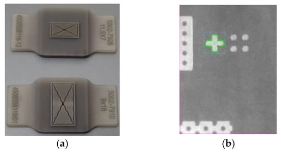
Figure 3.
(a) Customized thermodes for bonding the quartz cover and silicon die; (b) Alignment mark on substrate wafer under optimized light settings.
3. Device Testing
Experiments are conducted using whole blood diluted in 0.9% NaCl water solution at a dilution ratio of 1:200 (blood to water). The diluted blood was successfully transferred into the silicon chip and into the quartz imaging chamber, leading to red blood cells are clearly visible (see Figure 4). The propagation of the liquid-vapor interface of the capillary meniscus is studied using image processing techniques (see Figure 5). The experimentally determined velocity and position of the interface versus time agree well with models of capillary flow in a rectangular cross-section channel.
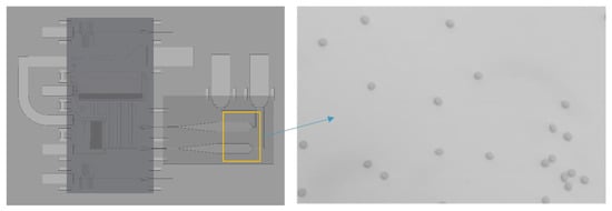
Figure 4.
Schematic of the chip with details of the imaging chamber area. Red Blood Cells are clearly visible in the imaging chamber area (zoom on the yellow square).
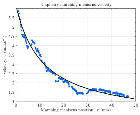
Figure 5.
Speed of the advancing liquid meniscus vs. position (test channel).
References
- Koczula, K.M.; Gallotta, A. Lateral flow assays. Essays Biochem. 2016, 60, 111–120. [Google Scholar] [CrossRef] [PubMed]
- Gervais, L.; Delamarche, E. Toward one-step point-of-care immunodiagnostics using capillary-driven microfluidics and PDMS substrates. Lab Chip 2009, 9, 3330–3337. [Google Scholar] [CrossRef] [PubMed]
- Dudek, M.M.; Lindahl, T.L.; Killard, A.J. Development of a point of care lateral flow device for measuring human plasma fibrinogen. Anal. Chem. 2010, 82, 2029–2035. [Google Scholar] [CrossRef] [PubMed]
Publisher’s Note: MDPI stays neutral with regard to jurisdictional claims in published maps and institutional affiliations. |
© 2018 by the authors. Licensee MDPI, Basel, Switzerland. This article is an open access article distributed under the terms and conditions of the Creative Commons Attribution (CC BY) license (https://creativecommons.org/licenses/by/4.0/).