Abstract
Micro particles and nanoparticles applied in microfluidics became a popular direction to improve biochip performance. Magnetic beads are the well-studied carriers including manipulation and surface modification, which could be easily to apply in biosensor development. A new methodology combined the actuators and sensor in the same chip all trigged by illumination is proposed in this study. A microfluidic chip with a-Si:H layer and ITO/glass with proper operation could be used to collect magnetic beads firstly and then following the optoelectrical measurement. In the meantime, 2D images for clusters of magnetic beads can be easily achieved with the addressable illumination. This proposed platform could own the high potential for a sensor array with better sensing performance.
1. Introduction
Magnetic beads had been widely investigated as the carrier for surface modification and drug delivery due to easy control, small size and high surface area [1]. Recently, many medical sensors combined with magnetic beads had delivered good performance in various applications including environmental [2], DNA [3], Alzheimer Disease [4], and E. coli. Detection [5]. Normally, the control of magnetic beads can be achieved by the modification of magnetic force. However, a new operation methodology is conducted to manipulate magnetic beads and measure the difference of surface potential based on the light-addressable potentiometric sensor (LAPS) in this study.
2. Materials and Methods
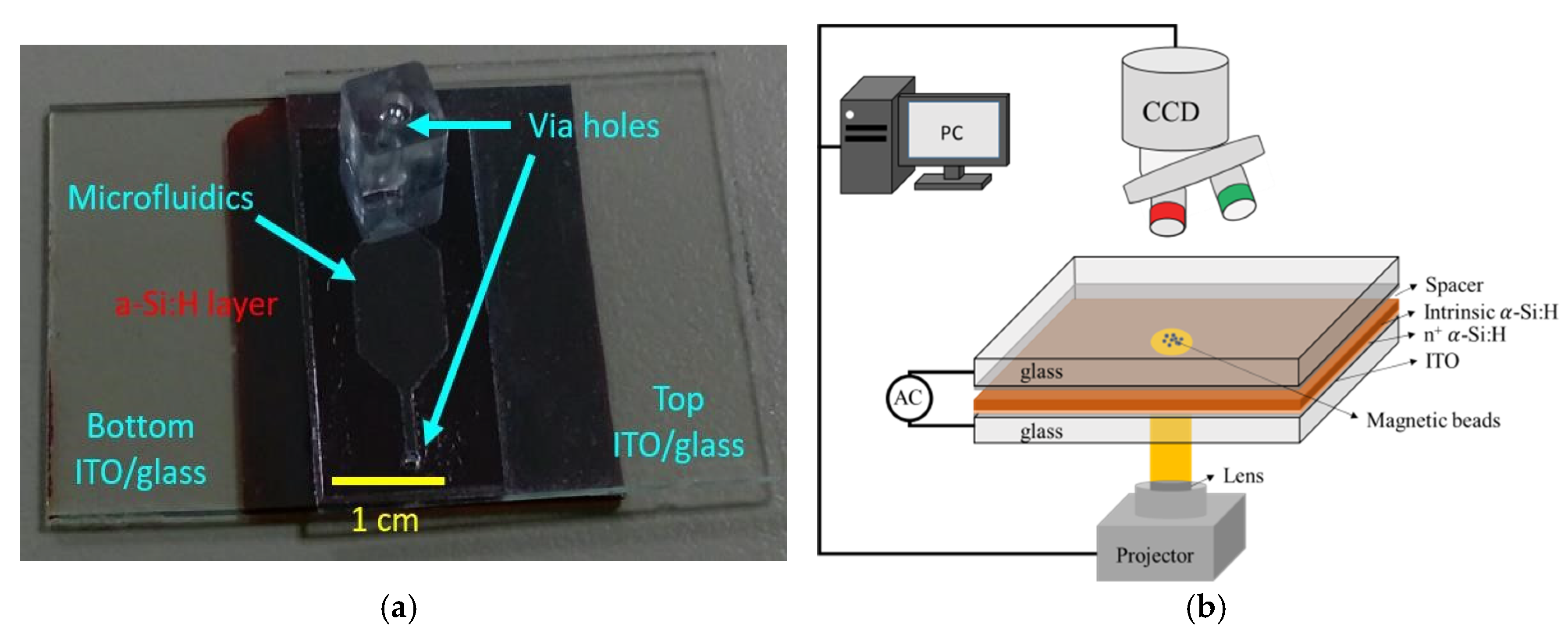
Hydrogenated amorphous silicon (a-Si:H) layer deposited on indium tin oxide (ITO)/glass had been proven as semiconductor layer of LAPS [6]. The a-Si:H layer was processed by high density plasma chemical vapor deposition (HDPCVD) in National Nano Device Laboratories (NDL) in Taiwan. Device structure was modified with adding microfluidics constructed by patterned glue tape with thickness of 60 µm and a top electrode of ITO/glass. 2 via holes were penetrated from top ITO/glass to make solution flow with magnetic beads as shown in Figure 1a. The schematic plot of optical manipulation system is shown in Figure 1b. CCD was used to record and observe manipulation process on the top of chip. Programmed patterns could be used to define the light patterns through projector and lens from the back side of chip. Light intensity is fixed during the manipulation. During the manipulation, top and bottom electrode of chip was applied with a ac bias of peak-to-peak voltage (Vpp) of 8 V.

Figure 1.
(a) Picture of real chip and (b) Schematic plot of operation setup.
3. Results & Discussion
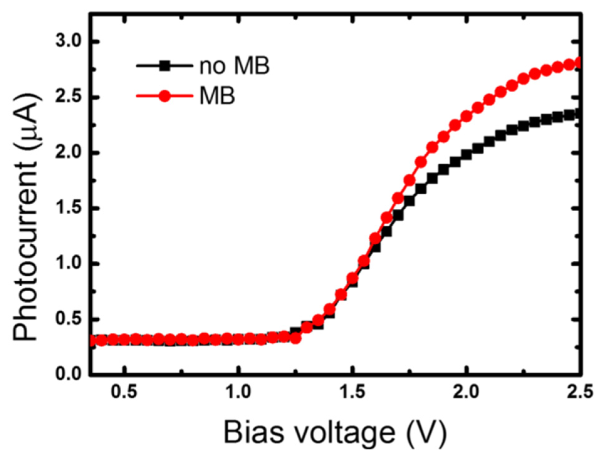
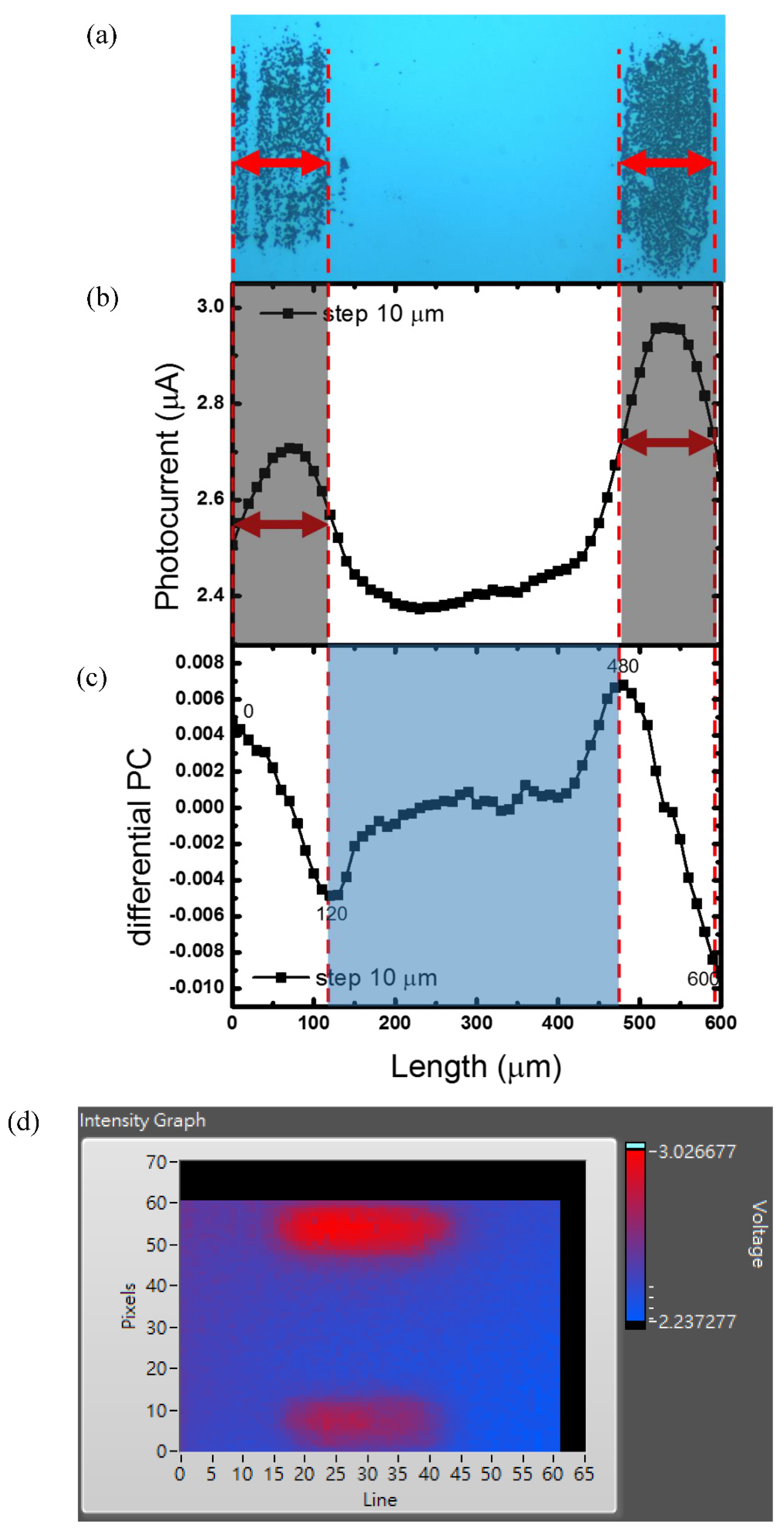
With the ac modulated sine wave applied between top and bottom electrode, the magnetic beads could be collected and moved with light patterns. With a certain bias setup and operation, magnetic beads could be collected. By using the LAPS measurement system with red laser integrated with XY stage [7], the photocurrent versus bias in different coordination can be collected. As shown in Figure 2, the photocurrent versus bias voltage curves measured in the area with and without magnetic beads are similar, but a clear higher photocurrent could be found in the area with magnetic beads in the inversion region. As shown in Figure 3a, 2 areas with magnetic beads are collected on the surface of a-Si:H layer. This chip was scanning by LAPS system by controlling the X-Y stage. Photocurrent versus scanning length could be seen in Figure 3b. It can be clearly seen that the high photocurrent shown in the area with magnetic beads. With the differentiation of photocurrent by scanning length, the distance of maximum and minimum value could be calculated as the length of area without magnetic beads. The resolution of photocurrent is not very good since the diameter of illumination are is about 150 μm. The basic photocurrent versus bias voltage of LAPS measurement could be seen in Figure 3d. This proposed methodology could be further integrated with the surface modification of magnetic beads and relative biomarker capture for the improvements of biosensor application.

Figure 2.
Photocurrent versus bias voltage for area with and without magnetic beads.

Figure 3.
(a) OM picture of attached magnetic beads, (b) photocurrent versus X-coordination curve. Gray area could be referred to area with magnetic beads. (c) differentiated photocurrent versus X-coordination curve. Blue area could be referred to area without magnetic beads. (d) 2D images directly measured from selfdeveloped LabVIEW program.
4. Conclusions
Magnetic beads can be fixed on the surface of a-Si:H layer by proper setting in the manipulation. The photocurrent difference by magnetic beads on the same chip can be also measured by LAPS system. A potential lab-on-a-chip is firstly presented by using a photoconductive semiconductor layer of a-Si:H with the ability of manipulation of magnetic beads and the measurement by LAPS. Further optimization of chip design and fabrication are suggested before real biomedical applications.
Author Contributions
C.-M.Y. and M.-H.W. conceived and designed the experiments; Y.-P.C. and J.-L.H. performed the experiments; H.-Y.P., M.-H.W., C.-M.Y. analyzed the data; H.-Y.P., M.-H.W., C.-M.Y. contributed reagents/materials/analysis tools; C.-M.Y. wrote the paper. All authors have read and agreed to the published version of the manuscript.
Acknowledgments
This research was partially supported by the Ministry of Science and Technology of the Republic of China under Contract no. MOST 105–2221-E-182-057-MY3.
Conflicts of Interest
The authors declare no conflict of interest.
References
- Gijs, M.A.M. Magnetic bead handling on-chip: New opportunities for analytical applications. Microfluid. Nanofluid. 2004, 1, 22–40. [Google Scholar] [CrossRef]
- Horák, D.; Babič, M.; Macková, H.; Beneš, M.J. Preparation and properties of magnetic nano- and microsized particles for biological and environmental separations. J. Sep. Sci. 2007, 30, 1751–1772. [Google Scholar] [CrossRef] [PubMed]
- Palecek, E.; Fojta, M. Magnetic beads as versatile tools for electrochemical DNA and protein biosensing. Talanta 2007, 74, 276–290. [Google Scholar] [CrossRef] [PubMed]
- Li, S.-S.; Lin, C.-W.; Wei, K.-C.; Huang, C.-Y.; Hsu, P.-H.; Liu, H.-L.; Lu, Y.-J.; Lin, S.-C.; Yang, H.-W.; Ma, C.-C.M. Non-invasive screening for early Alzheimer’s disease diagnosis by a sensitively immune magnetic biosensor. Sci. Rep. 2016, 6, 25155. [Google Scholar] [CrossRef] [PubMed]
- Freda, C.; Jacinta, G.; Huda, S.; Ahmed, M.; Rosilda, S. Advances in Screening, Detection and Enumeration of Escherichia coli Using Nanotechnology-Based Methods: A Review. J. Biomed. Nanotechnol. 2018, 14, 829–846. [Google Scholar]
- Yang, C.-M.; Liao, Y.-H.; Chen, C.-H.; Chen, T.-C.; Lai, C.-S. P-I-N amorphous silicon for thin-film lightaddressable potentiometric sensors. Sens. Actuators B Chem. 2016, 236, 1005–1010. [Google Scholar] [CrossRef]
- Yang, C.-M.; Zeng, W.-Y.; Chen, Y.-P.; Chen, T.-C. Surface modification for high photocurrent and pH sensitivity in a silicon-based light-addressable potentiometric sensor. IEEE Sens. J. 2018, 18, 2253–2259. [Google Scholar] [CrossRef]
Publisher’s Note: MDPI stays neutral with regard to jurisdictional claims in published maps and institutional affiliations. |
© 2018 by the authors. Licensee MDPI, Basel, Switzerland. This article is an open access article distributed under the terms and conditions of the Creative Commons Attribution (CC BY) license (https://creativecommons.org/licenses/by/4.0/).