Abstract
As a leading provider of sensing solutions ams AG is developing semiconductor sensors in a wide variety of fields. One of the key competences of ams AG lies in optical sensing. To widen the company’s portfolio in this field we have been developing processes for fully integrated CMOS compatible photonic components based on Si3N4 in the last few years. This contribution will give an overview of the Si3N4 process as a post-processing flow for standard CMOS, some basic photonic building blocks and their properties, and an example for their use in the field of medical applications.
1. Introduction
Already in the 1980s photonics came into common use in telecommunication using optical fiber technologies. In recent years, also a variety of photonic sensors has been proposed and developed. So far, one of the major drawbacks of most of these photonic devices, though, has been the lack of integration into existing (semiconductor) production processes. One way to overcome this limitation is to use SiN material systems to process monolithically integrated CMOS-compatible photonic sensors in the visible and near-infrared spectrum to form photonic integrated circuits (PICs) [1].
In this contribution, we will present the basic processing steps for the SiN photonic technology, several photonic components, as well as some of their applications. One possible application relates to the medical area, namely optical coherence tomography (OCT), a fast growing imaging technique in ophthalmology.
2. Materials and Methods
2.1. Wafer Processing
All wafers presented in this work were processed at ams’ FAB-B in Premstaetten, Austria. For the development of the waveguides and photonic structures, short-loop wafers without CMOS were prepared. These post-processing steps are fully compatible with CMOS processing and an overview of this process flow (indicating full CMOS integration) is given in Figure 1.
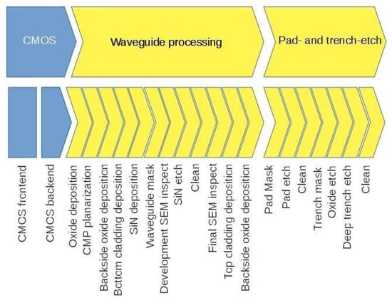
Figure 1.
Schematic of the post-processing flow for waveguide integration on CMOS wafers. Waveguides and photonic components are processed after CMOS front- and back-end and are finished with optional etching the pads and a deep trench on the edges of the PIC to facilitate butt-coupling with optical fibers.
After CMOS front- and back-end processing, SiO2 is deposited and planarized in several steps until a planar oxide surface functioning as bottom cladding for the waveguides is achieved. To compensate for stress-induced wafer bow, oxide is also deposited on the backside of the wafer several times. Above the bottom-cladding the waveguides and photonic structures are processed in following steps: deposition of SiN layer (typically 120–250 nm thickness); photolithographic masking; SEM inspection of the mask; SiN etching; SEM inspection of etched structures. Afterwards, a topcladding of several microns SiO2 is deposited. Finally, the pads are etched and- optionally—it is possible to etch deep trenches along the PIC’s edges, which yielded very smooth surfaces and low coupling losses to facilitate butt-coupling.
Using this process with photonic simulation based designs, several basic building blocks for photonic devices have been processed. These structures included straight waveguides combined with compact spirals of different lengths and radii to determine the propagation-, bend-, and coupling-losses. These loss measurements have been performed using butt-coupling of a polarization maintaining single mode fiber at the input and multimode fiber at the output of the devices. Besides simple waveguides, several other photonic building blocks including Y-branch splitters, polarization beam splitters, grating-couplers, or more complex devices such as arrayed waveguide gratings (AWGs, see Section 2.2) can be processed this way.
2.2. OCT Application
One application of integrated photonics relates to the medical area, namely optical coherence tomography (OCT), a fast growing imaging technique mainly used in ophthalmology. Drawbacks of existing OCT systems are their high costs as well as their bulkiness, which prevents wider spread of OCT systems. The monolithic integration of optical and electrical components on a single chip are a highly promising way to overcome both cost and size issues. One option towards higher integration in spectral-domain OCT [2] is the realization of a PIC with an arrayed waveguide grating (AWG) coupled to integrated photodetectors. Figure 2a shows a schematic of such a spectral-domain OCT as it is state-of-the-art today. Within the COHESION project it is the ultimate goal to integrate the interferometer, the AWG and photodetectors on a PIC to reduce the footprint and costs (Figure 2b). As an alternative approach, OCTCHIP aims for a swept source based OCT system.
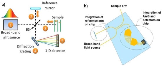
Figure 2.
Schematic of a spectral-domain OCT system (a) as of today including broad-band light source, beam-splitter, reference- and sample-arm, diffraction grating, and detector. In our work (b) the beam-splitter, reference arm, grating (AWG), and detectors are integrated on a PIC.
3. Results
Table 1 gives an overview of typical and best values for several loss sources of SiN waveguides processed as described in Section 2.1. Propagation loss at a wavelength of 850 nm was close to or even below 1 dB/cm for both TE and TM mode, respectively. Bend losses were typically at 0.025 dB per 90° bend at a minimum bend radius of 50 µm and 150 µm for TE and TM polarization, respectively. Coupling loss was typically around 1.3 dB for in- as well as out-coupling.

Table 1.
Typical and best values for TE/TM propagation-, bend- and coupling losses of SiN waveguides at λ = 850 nm.
Besides simple waveguides, several other photonic components are needed for OCT such as beam splitters and AWGs. Figure 3 for example shows the simulated and measured results of a broadband 2 × 2 coupler designed for 50:50 splitting ratios at 840 nm. Simulated and measured values are in excellent agreement with each other.
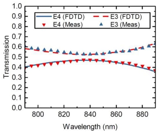
Figure 3.
Measured results and predicted values by 3D FDTD simulations for the wavelength dependence of the splitting ratio of a broadband 2 × 2 coupler designed for 50:50 splitting ratio at 840 nm (TE-like polarization).
Figure 4 shows another crucial component for SD-OCT, namely an AWG with—in this case- 8 channels. Here, the experimental performance deviates from simulations due to minor imperfections introduced through the process, which were not taken into account in the simulations. Nevertheless, the concept works well and will be further improved. AWGs with 8 channels have already been processed and characterized [3], AWGs with 40, 80 and 160 channels have been designed [2,3].
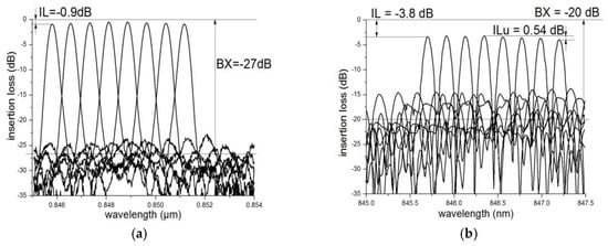
Figure 4.
Simulated (a) and measured (b) spectral response of an 8-channel AWG (from [3]).
4. Discussion
This paper shows a route towards monolithical integration of photonic components on CMOS technology using SiN based photonics. Basic photonic building blocks (waveguides, splitters) show excellent performance, more complicated structures such as AWGs still need some refinement but are in principle feasible with this PIC technology platform. The post-processing is compatible with CMOS technology, which allows for monolithic co-integration of photonics and optoelectronics on a single chip. The realization of such monolithically integrated PICs are further goals in the COHESION and the OCTCHIP project.
Author Contributions
M.S. wrote this paper and together with G.K. did the wafer processing, J.K. the project management at ams AG. P.M., S.N. and A.M. simulated and designed the waveguide building blocks and characterized the optical properties. R.H. and P.M. contributed on the conceptual and technical supervision level and did the project management at AIT. D.S. provided the simulations and designs for the multi-channel AWGs.
Acknowledgments
Part of this work was carried out in the framework of the project COHESION funded by the Austrian Research Promotion Agency (FFG), no. 848588. This work was also supported through the H2020 project OCTCHIP (contract number 688173) funded by the European Commission.
Conflicts of Interest
The authors declare no conflict of interest.
References
- Baets, R.; Subramanian, A.Z.; Clemmen, S.; Kuyken, B.; Biestman, P.; Le Thomas, N.; Roelkens, G.; Van Thourhout, D.; Helin, P.; Severi, S. Silicon photonics: Silicon nitride versus silicon-on-insulator. In Proceedings of the 2016 Optical Fiber Communications Conference and Exhibition, Anaheim, CA, USA, 20–24 March 2016; pp. 1–3. [Google Scholar]
- Seyringer, D.; Maese-Novo, A.; Muellner, P.; Hainberger, R.; Kraft, J.; Koppitsch, G.; Meinhardt, G.; Sagmeister, M. Design and Optimization of High-Channel Si3N4 based AWGs for Medical Applications. In Proceedings of the 6th International Conference on Photonics, Optics and Laser Technology, Funchal, Portugal, 25–27 January 2018; pp. 213–220. [Google Scholar]
- Seyringer, D.; Burtscher, C.; Edlinger, J.; Maese-Novo, A.; Muellner, P.; Hainberger, R.; Kraft, J.; Koppitsch, G.; Meinhardt, G.; Sagmeister, M. Design of 160-Channel Si3N4 based AWG-Spectrometer for Medical Applications. In Proceedings of the 2018 TechConnect World Innovation Conference and Expo, Anaheim, CA, USA, 13–16 May 2018; Volume 4, pp. 209–212. [Google Scholar]
Publisher’s Note: MDPI stays neutral with regard to jurisdictional claims in published maps and institutional affiliations. |
© 2018 by the authors. Licensee MDPI, Basel, Switzerland. This article is an open access article distributed under the terms and conditions of the Creative Commons Attribution (CC BY) license (https://creativecommons.org/licenses/by/4.0/).