Proceeding Paper

A Compact Robust OWLS System for Biosensing of Multiple Samples †

by
Mauricio Moreno-Sereno
1,2,*,
Nasser Darwish-Miranda
2,3,
Miquel Giménez-Conejo
2,
Francisco Palacio-Bonet
2,
Iván Bernat-Ubiaga
2 and
Albert Romano-Rodríguez
1,2
1
Institute of Nanoscience and Nanotechnology (IN2UB), Universitat de Barcelona (UB), c/Martí i Franquès 1, E-08028 Barcelona, Spain
2
Department of Electronics and Biomedical Engineering, Universitat de Barcelona (UB), c/Martí i Franquès 1, E-08028 Barcelona, Spain
3
Bioimaging Facility, IST Austria, 3400 Klosterneuburg, Austria
*
Author to whom correspondence should be addressed.
Presented at the Eurosensors 2018 Conference, Graz, Austria, 9–12 September 2018.
Proceedings 2018, 2(13), 863; https://doi.org/10.3390/proceedings2130863
Published: 28 November 2018
(This article belongs to the Proceedings of EUROSENSORS 2018)

Abstract

:
A compact multichannel and portable OWLS (Optical Waveguide Light Mode Spectroscopy) biosensor will be presented. With a sensitivity of 16.3°/RIU (degrees per refractive index unit) it incorporates on-line reference and high potential for further miniaturization.

1. Introduction

Among many other examples, medical diagnostics, the monitoring of food quality and environmental pollution, and drug screening [1] require analytical data from molecular binding events, especially target molecule concentrations. Label-free techniques avoid problems as the time consumed and sample compatibility issues common for fluorescence labelling. Biosensors address these issues and optical approaches in particular are considered highly sensitive and in most cases biocompatible [2].
In a wide range of applications it is also desirable to analyze simultaneously several samples or several targets from the same sample. For this purpose, optical biosensors are particularly suitable [3]. Nevertheless, the complexity of the instrumentation keeps the development of high-throughput biosensing devices under active development [4]. In addition, many applications require in-situ operation, which makes portability a highly desired feature. As an example, in 2017 the simultaneous detection of three different pathogenic bacteria using an optical biosensor was reported [5].
Two of the most sensitive optical biosensing techniques are Surface Plasmon Resonance (SPR) [5,6] and Optical Grating Coupling Biosensing (OGCB). For scientific applications, where the adsorbate might not be fully characterized, OGCB provides thickness and optical density information at the same time, which is an advantage over SPR [7].

2. Device Concepts

In OGCB devices the sensing parameter is the effective refractive index neff, which brings the phase speed at which the coupled light propagates through the waveguide. This index depends on the optical structure of the layer, and it is very sensitive to the mass adsorbed on its surface. Functionalizing this surface [8] the adsorption can be made specific for any molecule of interest. OGCB uses grating structures to monitor effective refractive indices through coupling resonances.
The relation between refractive indices and coupling angles is given by:
n eff = n ext sin ( θ c ) + m λ Λ
For a given wavelength λ the grating pitch Λ is chosen so that the only allowed diffractive order m is 1 (or −1). In this way only one coupling angle θc is allowed, bringing higher efficiencies and sensitivities. Although in general there’s no analytical expression for it, within small enough variation ranges, effective indices and coupling angles behave linearly on the attached mass.
The coupling angles can be measured after the out-coupling of the already coupled light [9] or by monitoring the insertion of light into the waveguide [7], as presented here. While the first option requires no moving parts the second allows a very close placement of the optomechanical components, which decreases the overall size of the system. Finally, we adapted the on-line reference setup presented in [10] to improve robustness and reliability of the results.

3. Materials and Methods.

3.1. Device Design and Fabrication Process

Due to a relatively high refractive index of 2.01 and CMOS-compatibility silicon nitride (Si3N4) was our preferred choice for a waveguiding layer. A fused silica (SiO2) wafer was chosen as a transparent, CMOS-compatible substrate, allowing light coupling through it instead of through the analysed liquid. A model based on the Equivalent Layer Approximation (ELA) [10] was used for optimizing the sensitivity dneff/dnextagainst the external refractive index. At a wavelength of 633 nm, 65 nm was the optimal thickness for the waveguide layer. 20 nm was a good compromise between sensitivity and technologic restrictions for the grating etching depth. These values allowed only one (TE0) propagation mode and diffractive orders of 0 (refraction, with no coupling) and ±1.
The fabrication process consisted in the following steps:
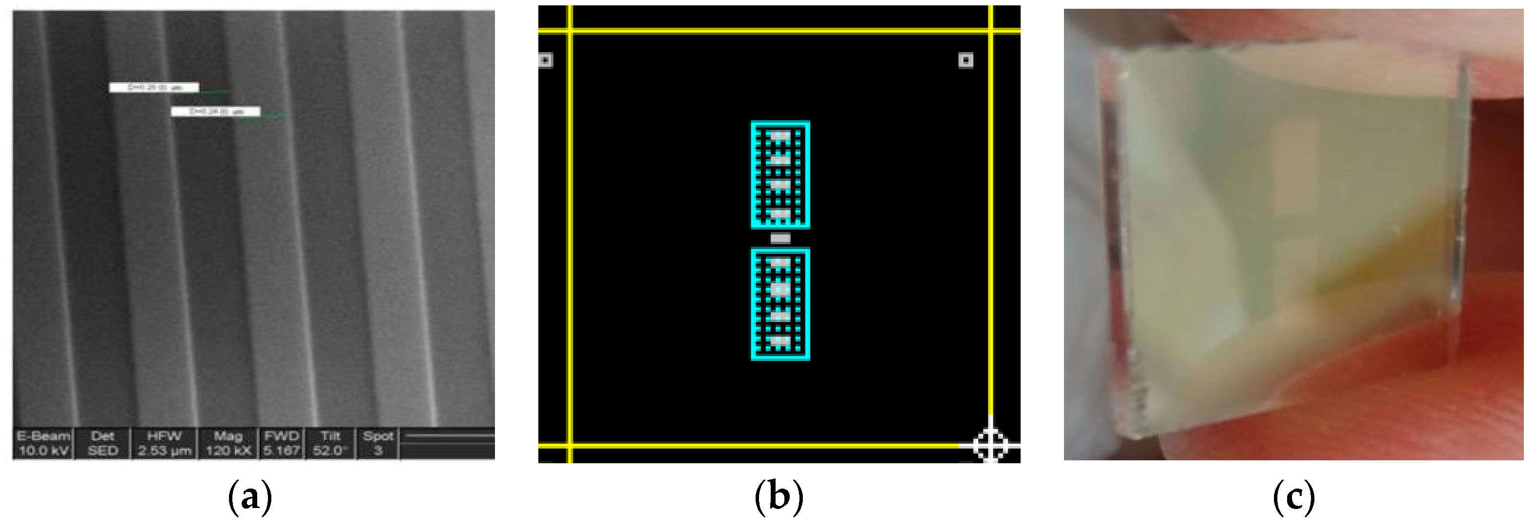
  • Deposition of 65 nm of Si3N4 on a fused silica (SiO2) wafer by Low Pressure Chemical Vapor Deposition (LPCVD), at 770 °C, for 18 min.
  • Grating patterning: a 0.5 µm pitch, 50% duty cycle grating was etched by Electron-Beam Lithography on a photoresist coating. After developing it the wafer was etched by Reactive Ion Etching at an Oxford Plasmalab 100 RIE facility for two minutes to obtain a grating depth of 20 nm (Figure 1a).
  • Plasma-Enhanced Chemical Vapor Deposition (PECVD) of a 510 nm SiO2 passivation layer, at 710 °C for 60 min, covering the full wafer.
  • Photolithographic definition and HF etching of the SiO2 passivation layer, opening the sensing windows (blue areas on Figure 1b). The central grating remained passivated to act as reference channel.

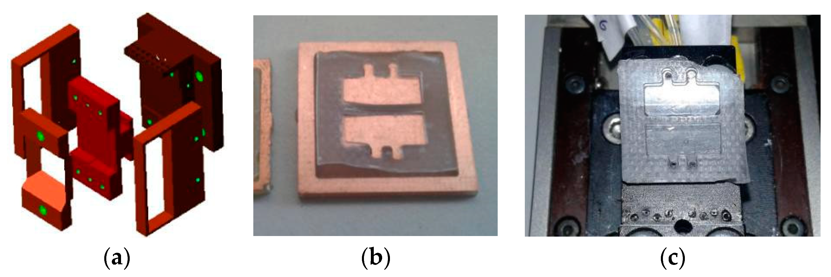
3.2. Holder Design and Fluidics

To allocate the sensor and the disposable PDMS gaskets an aluminum flow cell with 16 inlet/outlet ports (Figure 2a) was designed and fabricated. Figure 2b shows the filled DMS casting mold, made on a Printed Circuit Board (PCB). The resulting PDMS gasket, shown on Figure 2c had two chambers for bathing the top and bottom grating sets.

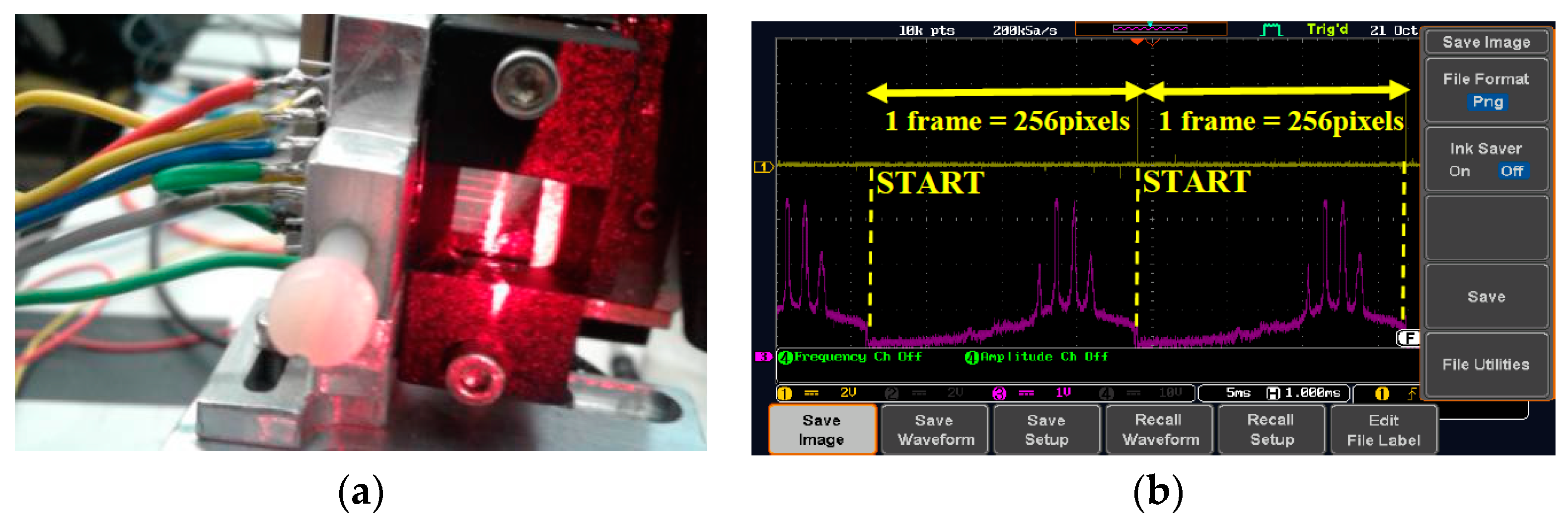
3.3. Instrumentation
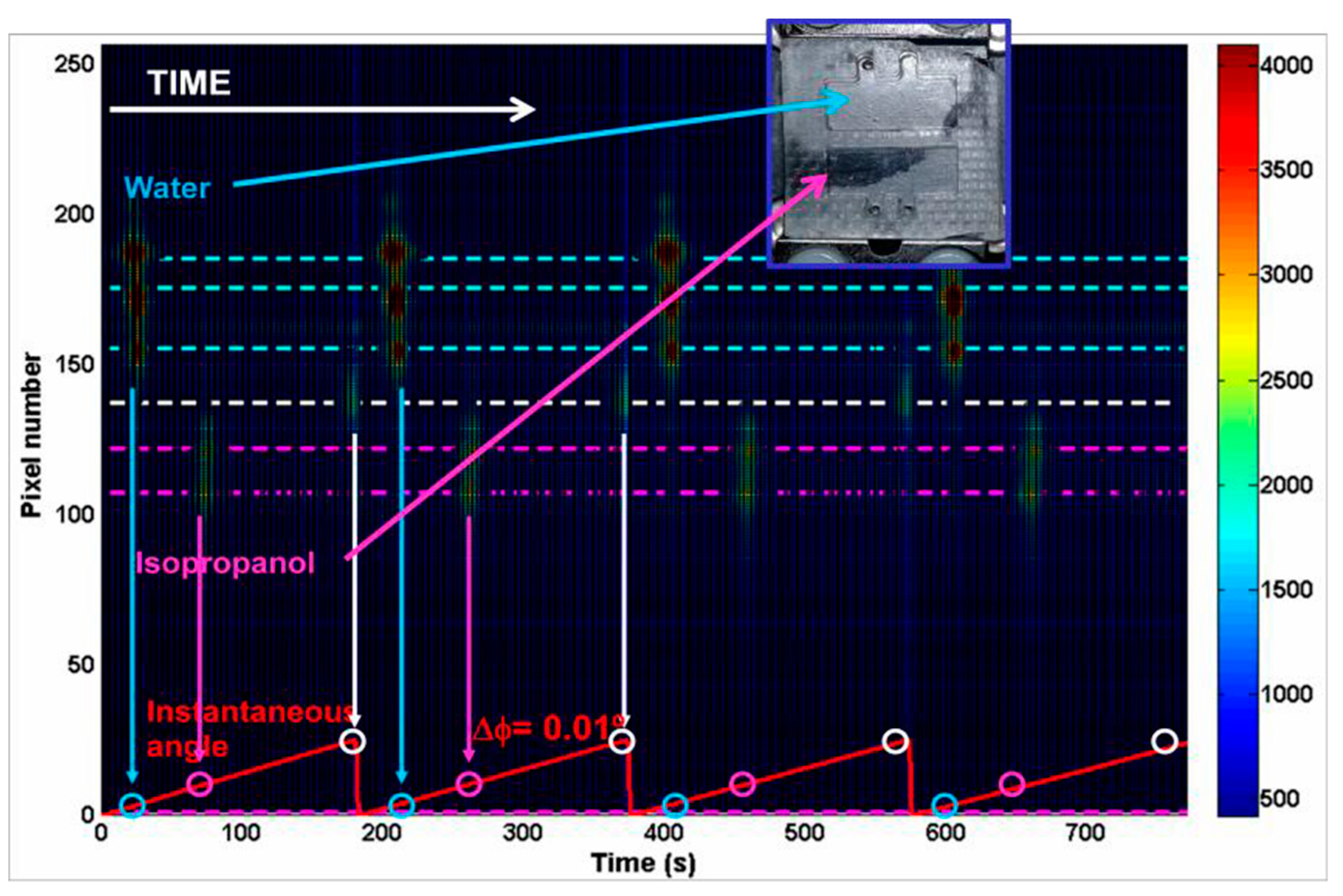
The sensing chip is inserted, with the fluidic gasket, in the cell described above. To scan the angular coupling resonances this cell is mounted on a SR50 compact high-resolution rotation stage-controlled by a SMC100CC single axis driver-, from Newport®. This allows a 0.01 degree scan step. A 633 nm He-Ne laser beam is expanded by a cylindrical lens to illuminate all the gratings at the same time. At the edge of the device a 256 pixel array (TSL1402 from TEXAS®) detects each coupled beam (Figure 3). Finally, a MSP430 microcontroller from TEXAS® transfers the signal to a MATLAB®-based custom software using the serial interface.

4. Results

Figure 4 shows an experiment where the upper gratings are immersed in water and the bottom ones are immersed in isopropanol. The red sawtooth line represents the instantaneous angle along time. 4 scan cycles across a range of 2.5 degrees are shown. The dotted cyan lines represent the center of the peaks for water (nH2O = 1.33) and the magenta ones correspond to isopropanol (nip = 1.38). The white line corresponds to the SiO2 reference channel (nSiO2 = 1.46). From the coupling angles a state of the art sensitivity of 16.3 degrees per refractive index unit [11] can be obtained.

5. Conclusions

A compact, low-cost multichannel OGCB device with built-in reference has been developed and tested for the simultaneous measurement of refractive indices. A sensitivity of 16.3°/RIU makes it adequate for biosensing, provided an appropriate surface treatment [10].

Author Contributions

M.M.-S. developed the optical system and measurements; N.D.-M. designed and fabricated optical devices and conceived the system; M.G.-C., F.P.-B. and I.B.-U. developed the electronics and A.R.-R. developed the fluidics.

Acknowledgments

This research has been founded by the Spanish Government through the projects TEC2009-12543 and TEC2013-48147-C6-1-R (AEI/FEDER, EU).

References

  1. Székács, I.; Kaszás, N.; Gróf, P.; Erdélyi, K.; Szendrő, I.; Mihalik, B.; Pataki, Á.; Antoni, F.A.; Madarász, E. Optical Waveguide Lightmode Spectroscopic Techniques for Investigating Membrane-Bound Ion Channel Activities. PLoS ONE 2013, 8, e81398. [Google Scholar] [CrossRef] [PubMed]
  2. Sun, Y.S. Optical Biosensors for Label-Free Detection of Biomolecular Interactions. Instrum. Sci. Technol. 2014, 42, 109–127. [Google Scholar] [CrossRef]
  3. Heideman, R.G.; Hoekman, M.; Schreuder, E. TriPleX-based integrated optical ring resonators for lab-on-a-chip and environmental detection. IEEE J. Sel. Top. Quantum Electron. 2012, 18, 1583–1596. [Google Scholar] [CrossRef]
  4. Zhang, X.; Liu, Y.; Fan, T.; Hu, N.; Yang, Z.; Chen, X.; Wang, Z.-Y.; Yang, J. Design and Performance of a Portable and Multichannel SPR Device. Sensors 2017, 17, 1435. [Google Scholar] [CrossRef]
  5. Zhang, X.; Tsuji, S.; Kitaoka, H.; Kobayashi, H.; Tamai, M.; Honjoh, K.I.; Miyamoto, T. Simultaneous Detection of Escherichia coli O157:H7, Salmonella enteritidis, and Listeria monocytogenes at a Very Low Level Using Simultaneous Enrichment Broth and Multichannel SPR Biosensor. J. Food Sci. 2017, 82, 2357–2363. [Google Scholar] [CrossRef] [PubMed]
  6. Homola, J.M. (Ed.) Surface Plasmon Resonance Based Sensors; Springer: Berlin/Heidelberg, Germany; New York, NY, USA, 2006; Volume 4. [Google Scholar]
  7. Voros, J.; Ramsden, J.J.; Csucs, G.; Szendro, I.; De Paul, S.M.; Textor, M.; Spencer, N.D. Optical grating coupler biosensors. Biomaterials 2002, 23, 3699–3710. [Google Scholar] [CrossRef]
  8. Banuls, M.J.; Puchades, R.; Maquieira, A. Chemical surface modifications for the development of silicon-based label-free integrated optical (IO) biosensors: A review. Anal. Chim. Acta 2013, 777, 1–16. [Google Scholar] [CrossRef] [PubMed]
  9. Tiefenthaler, K. Integrated optical couplers as chemical waveguide sensors. Adv. Biosens. 1992, 2, 261–289. [Google Scholar]
  10. Darwish, N.; Caballero, D.; Moreno, M.; Errachid, A.; Samitier, J. Multi-analytic grating coupler biosensor for differential binding analysis. Sens. Actuators B Chem. 2010, 144, 413–417. [Google Scholar] [CrossRef]
  11. Wei, X. Weiss, S.M. Guided mode biosensor based on grating coupled porous silicon waveguide. Opt. Express 2011, 19, 11330–11339. [Google Scholar] [CrossRef] [PubMed]
Figure 1. (a) SEM photograph of the fabricated diffraction grating with Λ = 0.5 µm; (b) Mask design of the nine-diffractive grating array. The blue rectangles correspond to the opening windows on the SiO2 passivation layer; (c) Photograph of the fabricated grating sensor showing the top and bottom, sensing areas. In the middle, the reference grating remains passivated.
Proceedings 02 00863 g001
Figure 2. (a) Aluminium flow cell; (b) casting mold for the PDMS, using printed circuit board (PCB) technology; (c) photograph of the fabricated PDMS fluidic gasket, showing the two chambers.
Proceedings 02 00863 g002
Figure 3. (a) Detail of the optical grating sensor with several coupled beams and the holder for the array of photodetectors on the left; (b) pixel array signal from 4 coupled beams.
Proceedings 02 00863 g003
Figure 4. Coupling for water and isopropanol: pixel intensity and angle (red line) vs. time.
Proceedings 02 00863 g004
Publisher’s Note: MDPI stays neutral with regard to jurisdictional claims in published maps and institutional affiliations.

