Abstract
A new Hall microdevice with minimal complexity and orthogonal magnetic field activation is suggested. The microsensor contains a rectangular n-type silicon substrate. On the long sides, three ohmic contacts are formed symmetrically and opposite each other. The first two opposite electrodes are connected and the second two are fed in the same way, and third ones are the outputs. The increased sensitivity constituting 40 V/AT is due to the reduced parasitic surface currents. Furthermore, output electrodes are moved out of the area where the supply currents flow. The 80 × 135 μm2 size of the sensor increases the resolution and provides detailed mapping of the magnetic field’s topology.
1. Introduction
The first three-contact (3C) silicon Hall sensor, activated by the magnetic field B parallel to the substrate’s plane, known also as a vertical or in-plane Hall element, was designed in 1983 by C. Roumenin and P. Kostov. It contains an n-Si plate with only three contacts on one of its sides—one central and two symmetrical to it. The end contacts through load resistors are connected to the central electrode via a supply source. Moreover, they constitute the output. The disadvantage of this single-ended microsensor is the decreased sensitivity resulting from the parasitic surface currents flowing between the contacts. Technological implementation is complicated because of the different-in-their-essence formation processes of the ohmic electrodes and load resistors. Vertical Hall elements represent a promising approach for implementing fully integrated 3D vector probes, as they have a multitude of applications in which the orthogonal activation by field B is preferred. This paper presents a transformation of a vertical Hall element into an orthogonal sensor configuration with minimal design complexity and a promising performance.
2. Device Structure and Operation
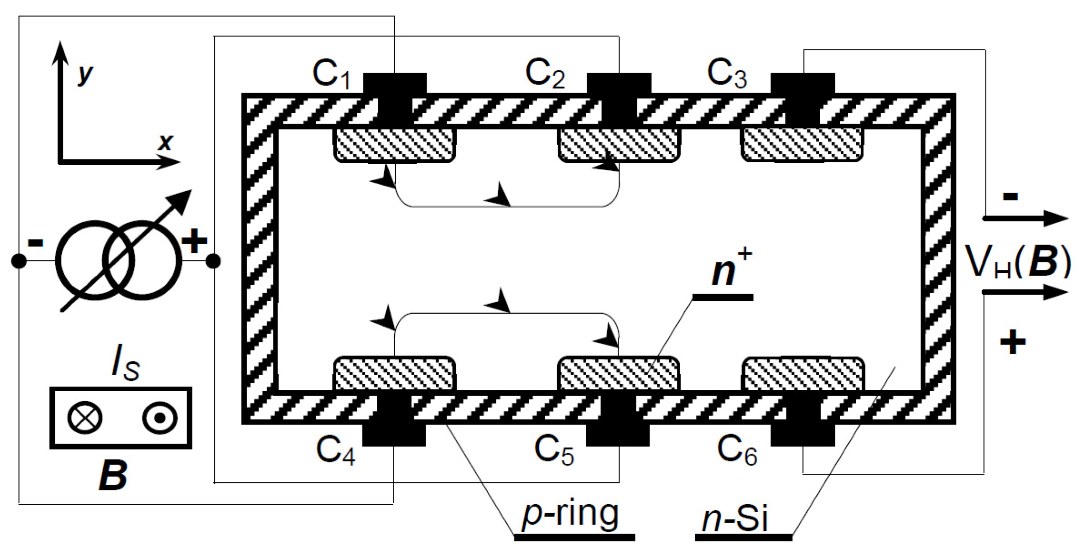
In Figure 1, the top view of the new Hall microdevice is shown. On the long sides of the thin n-Si substrate, two groups of three heavily doped n+ ohmic contacts, namely C1, C2, and C3 and C4, C5, and C6, respectively, are formed symmetrically and opposite to each other. The first two opposite electrodes are connected and the second two are fed in the same way; the third ones are the output. A deep surrounding p-ring is also present, which reduces the spreading of surface currents and confines the transducer region in the substrate. Contacts C3 and C6 of the sensor are those which are moved out of the areas where supply currents IC1,2 and IC4,5 flow. Field B is perpendicular to the plane, and electrodes C3 and C6 constitute the differential output VHC3,C6(B) ≡ VH(B). The operation is as follows. The supply contacts C1, C2, C4, and C5 are equipotential surfaces. As a result, the current lines IC1,2 and IC4,5 are initially perpendicular to them and penetrate deeply into the x-y area of the substrate. The field B leads to the Lorentz lateral deflection of the current paths in the x-y plane. They generate opposite-sign charges in the zones with contacts C3 and C6, i.e., VH(B). The specific two single Hall devices share the same active region. The elements with contacts C1, C2, and C3 and C4, C5, and C6, respectively, are controlled by the components IC2 and IC5. The increased sensitivity of the device results from the drastically reduced parasitic surface currents from the location of contacts C1 and C2 and C4 and C5 on the various long sides.
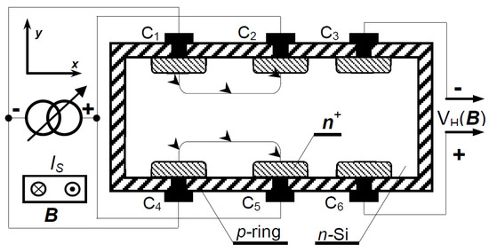
Figure 1.
Schematically plan-view of the new Hall configuration. In the x-y plane, the length of contacts C1–C6 is 30 μm, their width is 10 μm, and the depth is about 2 μm. The distance between electrodes C1, C2, and C4 varies: C5 is 20 μm, while lC2,3 and lC5,6 are 15 μm (on the mask). The width of the p-ring on the chip surface is about 20 μm.
3. Experimental Results and Conclusions
The prototype of the new configuration was manufactured using some of the processing steps applied in bipolar IC technology by employing four masks. The resistivity of the n-Si substrate is ρ ≈ 7.5 Ω·cm (ND = n0 ≈ 4 × 1015 cm−3). The penetration depth of the current trajectories into the x-y plane is about 30 μm. The active sensor zone is 80 × 135 μm2. The essential result is that the sensor is implemented within a single technological cycle. The output characteristics, VH(B), of the configuration are linear and odd when derived from field B and supply IS.
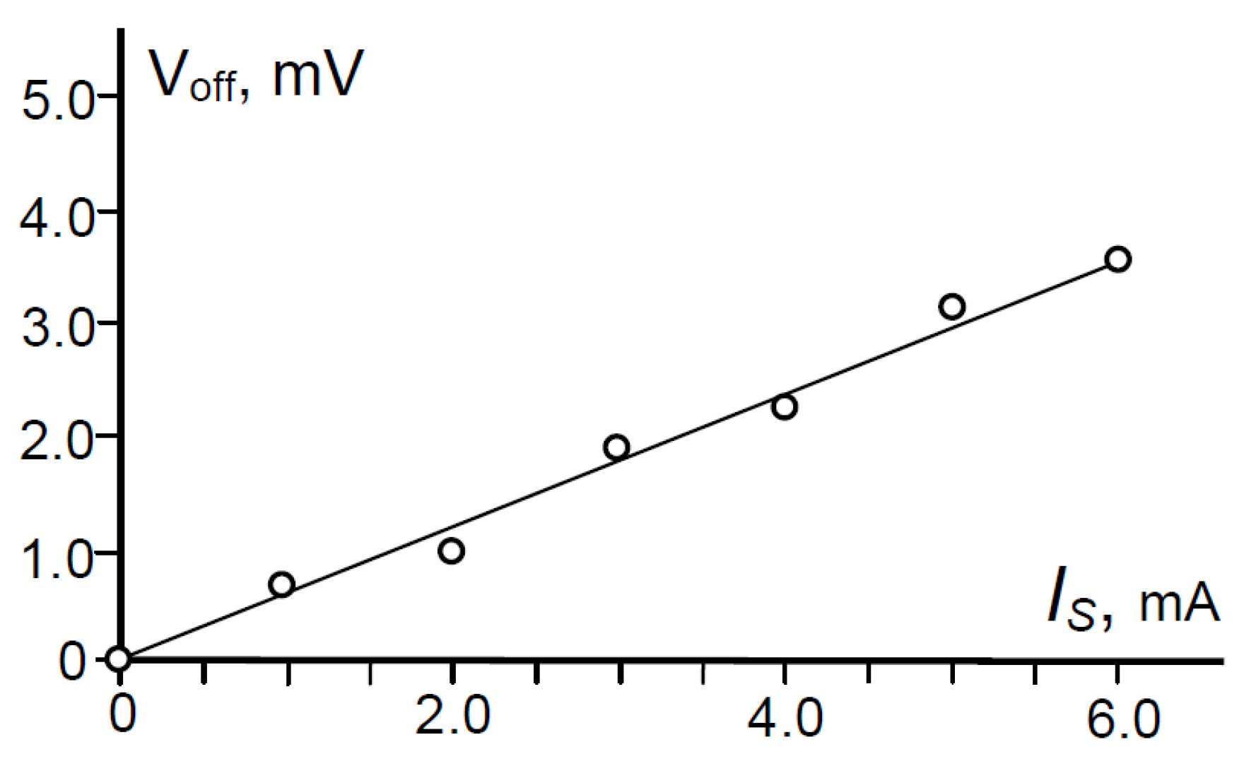
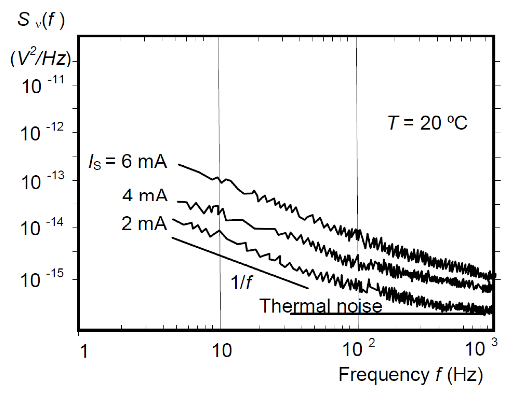
The sensitivity is SRI ≈ 40 V/AT. The nonlinearity constitutes no more than NL ≤ 0.2% in field B ≤ ±0.3 T and NL ≤ 0.6% in ±0.3 T ≤ B ≤ ± 0.7 T. According to the obtained data, the sensitivity temperature coefficient TCs is 0.1%/°C. It was established that the temperature coefficient of resistance R within the range 0 °C ≤ T ≤ 80 °C is approximately TCR ≈ 1.1%/°C. The initial offset of the new configuration is by about 25% lower than structures similar to the 3C microdevices. The offset voltage is a linear function of the current Is, Figure 2. The noise behaviour of the device is shown in Figure 3. At low frequencies, the spectrum f ≤ 1.0 kHz is typical for usual Hall plates, i.e., 1/f type. The extracted resolution in terms of the equivalent induction Bmin = [Sn,v(f)Δf2]/SA, [T] at current Is = 4 mA over bandwidth Δf = 5 Hz–400 Hz at the signal-to-noise-ratio S/N = 1 is around Bmin ≈ 16 µT.
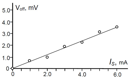
Figure 2.
Offset voltage versus bias of current IS at T = 20 °C.
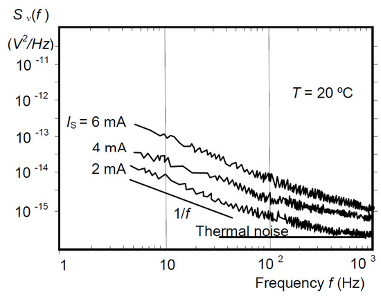
Figure 3.
Internal noise power spectral density with the current IS as a parameter.
In conclusion, the transformation of the 3C vertical Hall element into the orthogonal sensor configuration yields a high device performance, which is very promising for applications in automobiles, industrial control systems, consumer devices, and, especially, robotics and robotised surgery.
Author Contributions
Conceptualization, S.L. and C.R.; methodology, A.I. and M.R.; validation, S.L., M.R. and A.I.; investigation, S.L., M.R. and C.R.; resources, C.R.; writing—original draft preparation, S.L.; writing—review and editing, A.I. and C.R.; supervision, C.R.; project administration, S.L.; funding acquisition, C.R. and A.I. All authors have read and agreed to the published version of the manuscript.
Funding
This work was supported by CoC “Leonardo da Vinci”, Pleven under the Project № BG05M2OP001-1.002-0010-C01.
Institutional Review Board Statement
Not applicable.
Informed Consent Statement
Not applicable.
Data Availability Statement
Data are contained within the article.
Conflicts of Interest
The authors declare no conflicts of interest.
Disclaimer/Publisher’s Note: The statements, opinions and data contained in all publications are solely those of the individual author(s) and contributor(s) and not of MDPI and/or the editor(s). MDPI and/or the editor(s) disclaim responsibility for any injury to people or property resulting from any ideas, methods, instructions or products referred to in the content. |
© 2024 by the authors. Licensee MDPI, Basel, Switzerland. This article is an open access article distributed under the terms and conditions of the Creative Commons Attribution (CC BY) license (https://creativecommons.org/licenses/by/4.0/).