Abstract

Flexible, Fan-Out, Wafer-Level Packaging Using Polydimethylsiloxane and Printed Redistribution Layers †

1
Silicon Austria Labs GmbH, A-9500 Villach, Austria
2
Institut für Intelligente Systemtechnologien, Alpen Adria University, A-9020 Klagenfurt, Austria
*
Author to whom correspondence should be addressed.
Presented at the XXXV EUROSENSORS Conference, Lecce, Italy, 10–13 September 2023.
Proceedings 2024, 97(1), 153; https://doi.org/10.3390/proceedings2024097153
Published: 7 April 2024

Abstract

:
The hybrid integration of electronics in flexible substrates using fanned-out, wafer-level packaging (FOWLP) has recently gained significant attention, with numerous applications in wearable electronics, foldable displays, robotics, medical implants, and healthcare monitoring. In this study, a fully additive and scalable manufacturing process flow to realize a low-cost, flexible FOWLP system was introduced. Here, the integration of 36 LED chips in a biocompatible polydimethylsiloxane (PDMS) substrate was demonstrated using a stencil-printed silver (Ag) redistribution layer (RDL). The processes for the integration of chips, i.e., chip first (exposed die embedding), chip first (deep embedding with filled valleys) and chip last (RDL first), were implemented, and the corresponding samples were evaluated electrically. The bendability of the samples was also characterized at different bending diameters. Conclusively, it was shown that by using surface-modified PDMS as a flexible substrate and stretchable Ag paste as interconnect, flexible FOWLP can be produced.

1. Introduction

The continuous, large-scale advancement of flexible hybrid electronics (FHEs) towards producing high-performance and reliable products with a smaller footprint and lower cost is highly dependent on micro-assembly and rigid/flex integration technologies [1]. In fact, advanced microelectronic packaging technologies, such as chip embedding and 2.5D and 3D integrations, can provide significant benefits to FHEs. One of the most recent packaging trends in microelectronics is fanned-out wafer-level packaging (FOWLP). Known good bare dies are embedded into a rigid epoxy mold compound to form a reconfigured wafer for FOWLP. On the reconfigured wafer, a redistribution layer (RDL) is applied using photolithographic, sputtering and plating processes, which routes the die through the space around and on the die. FHEs using FOLWP have been recently investigated by many researchers, and several FHE demonstrators have been produced using this approach. Here, a flexible molding compound such as polydimethylsiloxane (PDMS) is employed as the substrate [2]. In our previous studies, additive manufactured RDLs were proposed for rigid FOWLP using different printing technologies [2]. In this study, fully additive, manufactured FOWLP is developed using spin-coated PDMS as the substrate and printed Ag paste tracks as the RDLs.

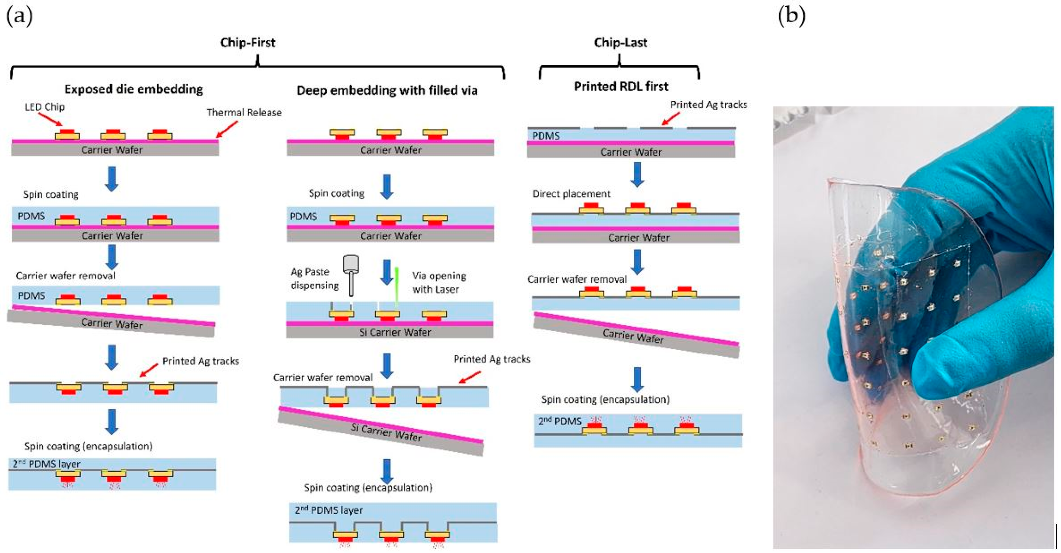
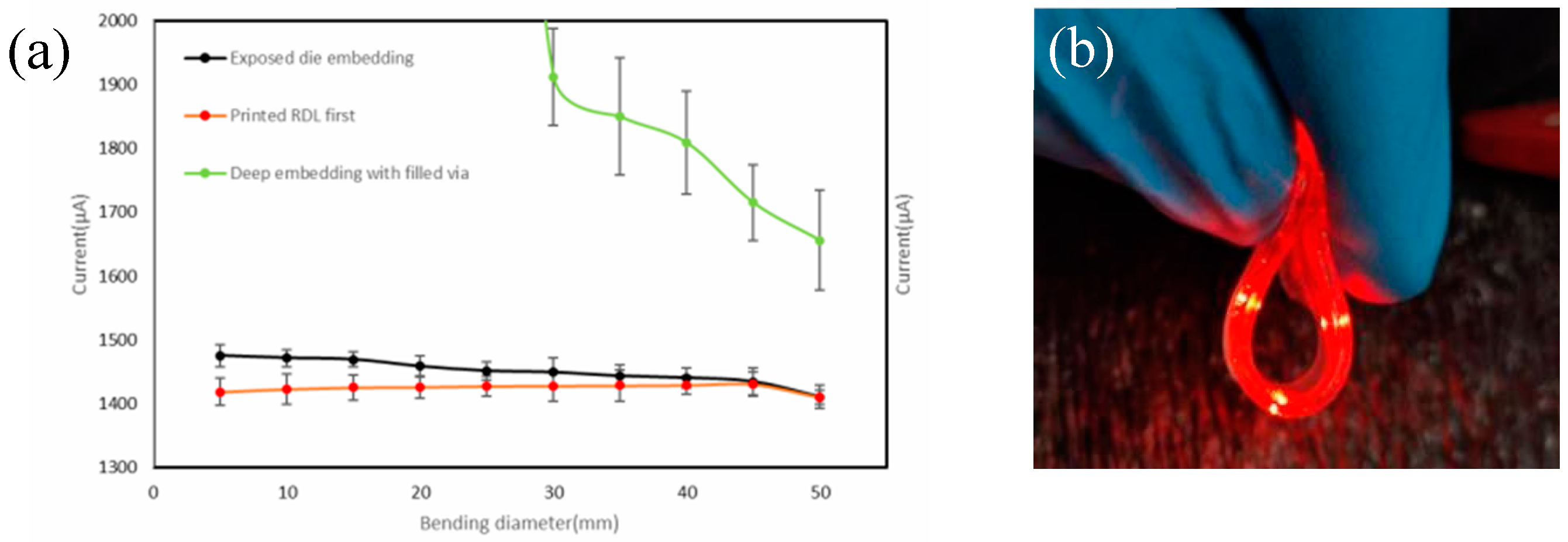
2. Results and Discussions

Three approaches were investigated in this study, as shown in Figure 1a. In the first approach (exposed die embedding), an array of 36 LEDs were embedded in PDMS (Sylguard 184). Thermal release tape (RT-A4098, Mitsui Chemicals, Minato City, Tokyo, Japan) was laminated to a 4-inch Si carrier wafer, and the LEDs were precisely placed on the tape using a die bonder. Afterwards, the PDMS was spin-coated and cured at 100 °C for 20 mins. The metallic interconnects (RDLs) were stencil-printed using stretchable Ag paste (Dycotec, Calne, UK). To enhance the adhesion of the Ag paste to PDMS, a UV ozone treatment was performed for 5 mins before printing. After the printing step, the Ag ink was cured and sintered at 100 °C in an oven. In the second approach (deep embedding with filled via), the chips were fully embedded in PDMS. Later, the contact pads of the LEDs were opened using a picosecond laser, followed by filling the vias with the same paste. In the third approach (chip last), the stencil printing was performed prior to the chip placement. The uncured Ag paste was tacky enough to secure chip contacts during processing, acting as a conductive adhesive. To enhance the reliability of the samples, another layer of PDMS was spin-coated as an encapsulation layer to reduce the stresses while bending. Figure 1b shows a demonstration of the embedded LED array.
After fabrication, the samples were characterized electrically at different bending diameters from 5 to 50 mm using a vernier caliper. The change in current was set as the criterium to detect if bending has any effect on the electrical interconnections of the LEDs. As seen in Figure 2a, there was a negligible change (~100 µA) in the current values as the loop diameter decreased. This was consistent for both the “exposed die embedding” and “chip last” approaches. On the other hand, in the “deep embedding” approach, the current increased significantly compared to that of the other approaches followed, by failure (LED light off) below a 30 mm loop diameter. This large variation in electrical current can be attributed to the poor electrical contact between the via and the LED pad. Figure 2b shows an image of a bent sample with powered LEDs. As a result, it was determined that both the “exposed die embedding” and “chip last” approaches fulfill the bendability requirements and can promise more reliable FHE systems.

Author Contributions

Conceptualization, M.H.M., M.K., S.K. and A.R. methodology, M.H.M., M.K., S.K. and A.R.; investigation, M.H.M., M.K. and S.K.; resources, A.R.; writing—original draft preparation, M.H.M., M.K., S.K. and A.R.; writing—review and editing, M.H.M., M.K., S.K. and A.R.; visualization, M.H.M., M.K., S.K. and A.R.; supervision, A.R.; project administration, A.R.; funding acquisition, A.R. All authors have read and agreed to the published version of the manuscript.

Funding

This work has received funding from the “European Regional Development Fund” (EFRE) and “REACT-EU” by the “Kaerntner Wirtschaftsf örderungs Fonds” (KWF) within the project Pattern-Skin (16048/34262/49709).

Institutional Review Board Statement

Not applicable.

Informed Consent Statement

Not applicable.

Data Availability Statement

Data are available upon request from authors.

Conflicts of Interest

The authors declare no conflict of interest.

References

  1. Iyer, S.S.; Alam, A. Flexible Hybrid Electronics Using Fan-Out Wafer-Level Packaging. In Embedded and Fan-Out Wafer and Panel Level Packaging Technologies for Advanced Application Spaces: High Performance Compute and System-in-Package; John Wiley & Sons: Hoboken, NJ, USA, 2021; pp. 233–260. [Google Scholar]
  2. Roshanghias, A.; Ma, Y.; Dreissigacker, M.; Braun, T.; Bretthauer, C.; Becker, K.-F.; Schneider-Ramelow, M. The Realization of Redistribution Layers for FOWLP by Inkjet Printing. Proceedings 2018, 2, 703. [Google Scholar] [CrossRef]
Figure 1. (a) The three approaches to realize flexible FOWLP; (b) an example of the demonstrator.
Proceedings 97 00153 g001
Figure 2. (a) Electrical characterization of the fabricated samples at different loop diameters. (b) A demonstration of the lighting LEDS under bending condition.
Proceedings 97 00153 g002
Disclaimer/Publisher’s Note: The statements, opinions and data contained in all publications are solely those of the individual author(s) and contributor(s) and not of MDPI and/or the editor(s). MDPI and/or the editor(s) disclaim responsibility for any injury to people or property resulting from any ideas, methods, instructions or products referred to in the content.

