Abstract
In this work, the fabrication of wafer-level vacuum-packaged 3C-SiC on Si double- clamped beam resonators via glass–silicon anodic bonding using Ti-based vacuum gettering is reported. Open-loop resonance measurements are performed on the vacuum-packaged devices, showing Q-factor values up to 290,000, a process yield above 80%, and a maximum vacuum level around 10−2 mbar inside the Ti-gettered encapsulations.
1. Introduction
Q-factor is an important parameter for the performance of a sensor based on mechanical resonance because it is strictly correlated with the measurement resolution that can be reached by any kind of sensing based on mechanical resonance frequency shifts [1,2]. We present here a technology for fabricating wafer-level vacuum-packaged SiC resonators with a high Q-factor.
2. Materials and Methods
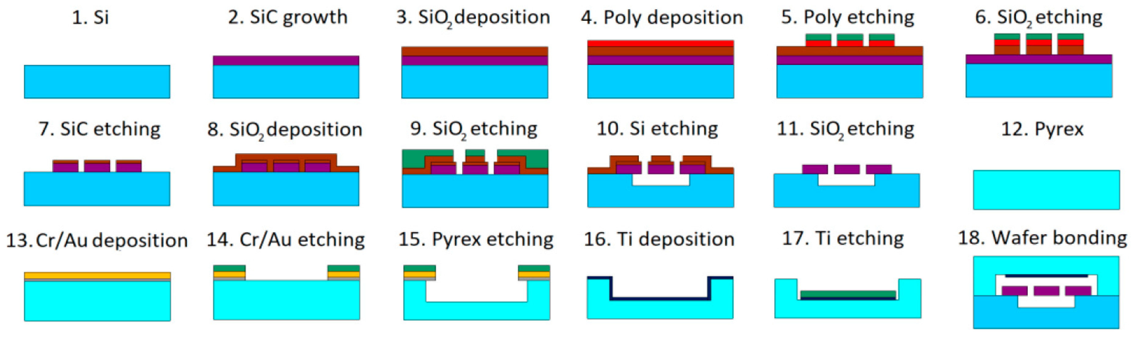
A hetero-epitaxial, non-intentionally doped 0.8 µm thick 3C-SiC thin film was grown on 500 µm thick <100> p-type silicon substrates using chemical vapor deposition, as described in [3]. The process flow adopted to fabricate the wafer-level vacuum-packaged SiC double-clamped beams is shown in Figure 1.
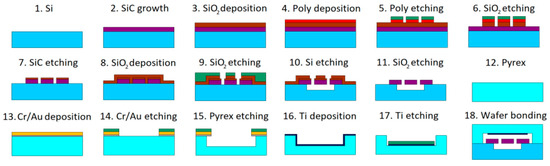
Figure 1.
Process flow for the fabrication of the wafer-level vacuum-packaged SiC resonators.
More details about the method used for the micromachining of the SiC structures can be found in [3]. Wet etching using a Cr/Au mask was used to produce 100 μm deep cavities in borosilicate glass for the encapsulation. In some of them, a 1 μm thick Ti layer was inserted for vacuum gettering using either lithography and wet etching or shadow masking in different dies on the wafer. The glass and Si wafers were bonded anodically at 400 °C after a 2 h degassing in vacuum (step 18 in the figure). The double-clamped beams were 900 μm long and 24 μm wide. Q-factor measurements were performed using a laser diode to induce a sinusoidal vibration of the beam, while a Doppler vibrometer was employed to measure the beam vibration at resonance.
3. Discussion
The results of the Q-factor measurements performed within encapsulations of different geometries are shown in Figure 2. Evidently, the presence of Ti greatly increases the vacuum level and the Q-factor, both when using shadow masking and the lithographic patterning of it. A very high yield of the vacuum encapsulation is also observed, with a vacuum level, estimated through the resonators’ Q-factor, around 10−2 mbar.
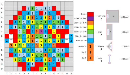
Figure 2.
Q-factor measurements performed on double-clamped beams inside capsules with different geometries and areas.
Author Contributions
Conceptualization, S.S., L.B., M.F., I.E., M.Z., F.L.V. and A.R.; methodology, S.S., L.B., M.F., I.E., M.Z., F.L.V. and A.R.; validation, S.S., L.B., M.F., I.E., M.Z., F.L.V. and A.R.; writing—original draft preparation, S.S., L.B., M.F., I.E., M.Z., F.L.V. and A.R. All authors have read and agreed to the published version of the manuscript.
Funding
This project has received funding from the European Union’s Horizon 2020 research and innovation programme under grant agreement No 863220.
Institutional Review Board Statement
Not applicable.
Informed Consent Statement
Not applicable.
Data Availability Statement
The datasets presented in this article are not readily available because the data are part of an ongoing study.
Acknowledgments
The contribution of Giulio Pizzochero, Filippo Bonafè, Fabrizio Tamarri, and Michele Sanmartin in the clean room processing of the samples is acknowledged.
Conflicts of Interest
The authors declare no conflicts of interest.
References
- Belsito, L.; Ferri, M.; Mancarella, F.; Masini, L.; Yan, J.; Seshia, A.A.; Soga, K.; Roncaglia, A. Fabrication of high-resolution strain sensors based on wafer-level vacuum packaged MEMS resonators. Sens. Actuators A Phys. 2016, 239, 90–101. [Google Scholar] [CrossRef]
- Belsito, L.; Bosi, M.; Mancarella, F.; Ferri, M.; Roncaglia, A. Nanostrain Resolution Strain Sensing by Monocrystalline 3C- SiC on SOI Electrostatic MEMS Resonators. J. Microelectromech. Syst. 2019, 29, 117–128. [Google Scholar] [CrossRef]
- Sapienza, S.; Ferri, M.; Belsito, L.; Marini, D.; Zielinski, M.; La Via, F.; Roncaglia, A. Measurement of residual stress and Young’s modulus on micromachined monocrystalline 3C-SiC layers grown on <111> and <100> silicon. Micromachines 2021, 12, 1072. [Google Scholar] [PubMed]

Disclaimer/Publisher’s Note: The statements, opinions and data contained in all publications are solely those of the individual author(s) and contributor(s) and not of MDPI and/or the editor(s). MDPI and/or the editor(s) disclaim responsibility for any injury to people or property resulting from any ideas, methods, instructions or products referred to in the content. |
© 2024 by the authors. Licensee MDPI, Basel, Switzerland. This article is an open access article distributed under the terms and conditions of the Creative Commons Attribution (CC BY) license (https://creativecommons.org/licenses/by/4.0/).