Abstract
Additive manufacturing (AM) technologies for metallic materials allow for the manufacturing of high-performance components optimised in weight, geometry, and mechanical properties. However, several post-processing operations are needed after production, including removing parts from the build platform. This operation is essential and must be performed rapidly, precisely, and with a good surface finishing. This work presents an experimental investigation of the wire electric discharge machining (W-EDM) process of Ti6Al4V specimens produced by AM technologies. The influence of cutting parameters is analysed compared to the material produced by conventional technology. Models of cutting speed and surface roughness obtained by a W-EDM are inferred from the collected data. Remarkably, the results show that the manufacturing process used to produce the components plays a crucial role in defining the final surface roughness and the most significant parameters affecting the machining performance.
1. Introduction
Wire-electric discharge machining (W-EDM) is an electro-thermal non-conventional machining process used to machine hard-to-cut materials. An electrical circuit is created between two electrodes, the workpiece and the wire tool, separated by a dielectric fluid, typically deionised water. The process consists of recurring sparks when an electrical voltage is applied between the workpiece and the wire [1]. Where the discharge takes place, the material is removed by evaporation or ejection in the liquid phase. The removed material cools down rapidly because of the presence of deionised water and solidifies into small spherical particles, called debris, which are flushed away by the dielectric fluid [2]. On the surface of the workpiece, small craters can be observed where the material has been removed. The presence of such craters defines the technological signature left by W-EDM machining. Because of the absence of mechanical contact between the two electrodes, no cutting tool forces are created while machining [2]. Therefore, only the workpiece electrical and thermal properties are relevant for the process [3]. This aspect allows for its use with difficult-to-cut materials [4] and represents one of the most significant advantages of W-EDM over other cutting machining processes.
Commonly, the absence of both wire breakage and spark indicates stable process conditions [5], and quantitative indicators such as the material removal rate (MRR), the cutting speed (Vc), and the surface roughness of the machined workpiece (SR) are used to measure the process characteristics under specific processing parameters. As an example, combination of high pulse on-time (ton) and discharge current (I) make the process faster, but is detrimental to the surface roughness, the kerf width (KW), and the wire wear ratio (WWR) [6,7,8,9,10,11,12,13,14]. Higher pulse off-time (toff) values lower the MRR and the cutting speed, but are beneficial for the surface roughness [15,16,17,18]. However, in some cases, the surface roughness worsens over a certain toff value [19,20]. Higher servo voltage (SV) values increase KW and enhance the surface finishing, but reduce the MRR, the cutting speed, and the WWR [6,13,18,21,22,23,24,25,26,27,28]. Higher open-circuit voltage (V) causes higher MRR, cutting speed, KW, and surface roughness [29]. Other factors, such as wire feed rate (WF), wire tension (WT), and dielectric pressure (DP), or dielectric flow rate, less significantly affect the W-EDM performance [27,28,29,30,31,32]. The workpiece thickness has been scarcely investigated, although it has been demonstrated to affect the process results [31,33]. A cross-comparison among the literature studies revealed some contrasting findings. For example, some work [10,17,21] demonstrated that higher toff values could reduce the surface roughness, but the opposite result has been shown in refs. [19,20]. In addition, material processing technology has never been considered as a determining factor.
However, using different processing technologies may affect the W-EDM performance, especially in the case of additive manufacturing (AM), which can process conventional metallic materials using a completely new approach. On the other hand, the advent of AM for metallic components led to significant W-EDM development and market growth. In fact, W-EDM is the preferable option for removing additive manufactured parts from the build platform onto which they were produced. However, few studies have investigated the working conditions during the W-EDM of AM parts [34,35], and these have focused only on specimens of AlSi10Mg and produced by laser powder bed fusion (PBF-LB) based AM systems [34,35].
This work investigates the performance of W-EDM when cutting the same nominal material, Ti6Al4V, produced with different processing technologies: casting, PBF-LB, and electron beam powder bed fusion (PBF-EB). The quality of the cut surface is evaluated using the surface roughness index, while the process efficiency is evaluated using the cutting speed. The effects of the process parameters, including the workpiece thickness, on these indexes are analysed using descriptive and inferential statistical tools, and regression models are inferred from the collected data.
2. Materials and Methods
2.1. Design of the Artefacts and Production
The artefact consists of three parallelepipedal sections of dimensions: 10 mm × 10 mm, 20 mm × 20 mm, and 30 mm × 30 mm, respectively, and the thickness of each section is 15 mm, corresponding to the cutting length. A replica of the artefact has been produced using an EOSINT M270 Dual Mode machine, an PBF-LB system, and an Arcam A2X, an PBF-EB system. For the PBF-LB and PBF-EB processes, the same nominal chemical composition of Ti6Al4V powder was used. The average particle size was 45 µm and 75 µm for the EOSINT and Arcam systems, respectively.
Figure 1 depicts the artefact geometry with the build direction (z-axis), the used machines, and the as-built artefacts. The process parameters are collected in Table 1 and Table 2. After the production, the replicas were cleaned from loose powder. In addition, the PBF-LB artefact has been subjected to stress-relieving treatment (in a furnace at 800 °C for 2 h). For the casting samples analysis, three commercial Ti6Al4V plates that copy the three parallelepipedal sections of the AMed artefact have been used for the analysis.
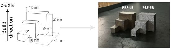
Figure 1.
Workpiece geometry and production.

Table 1.
PBF-LB process parameters [36].
Table 2.
EB-BPF process parameters [37].
2.2. Design of Experiment (DoE)
The machining was performed using a BAOMA DK7732 machine, a 4-axes high-speed feed W-EDM machine supplied by Suzhou Baoma Numerical Control Equipment Co. Ltd., Suzhou, China. The machine is equipped with a CNC pulse generator, a dielectric fluid supply system, a working table, a wire electrode drive and supply system, and a separate controller through which it is possible to adjust or modify the machine and the process parameters. A molybdenum wire electrode with a 0.18 mm diameter is reciprocally fed and used in the working area at high speed to limit the wire wear.
In light of the literature analysis, the selected parameters were: discharge current (I), pulse on-time (ton), pulse off-time (toff), and workpiece thickness. From the literature, it is well known that I and ton should be selected according to the workpiece layer thickness.
However, because standard W-EDM machine does not include adaptive control and additively manufactured components often include variable thicknesses, the evaluation of the effect of I and ton together with the thickness on W-EDM performance indexes were considered extremely important.
The W-EDM system used for the experiments does not allow for the control of toff directly and independently from ton. The relationship between the actual value of toff and ton is presented in Equation (1), in which toff* is a multiplicative coefficient that can vary from 1 to 30.
For this reason, the investigation of toff was replaced by selecting three levels of duty cycle (DC) (Table 3). DC is defined as the percentage of the active phase duration (ton) with respect to the total cycle time (Equation (2)) [38].
Table 3.
Investigated process parameters and their levels.
Consequently, toff* was selected accordingly to maintain the DC constant (Table 3). A full factorial designed plan was implemented, considering three levels for each process parameter (factor) for a total of 81 experimental runs.
The dielectric used was a solution made of deionised water and an additive provided by the machine producer, whose commercial name is BM-4. The open circuit voltage was kept to 80 V during all experiments, and the wire feed speed was kept at the maximum level, corresponding to 11 m/s. All experimental trials were randomised to reduce the systematic effects of uncontrolled variables, such as wire wear. The runs were repeated using the same process conditions for each artefact replica produced by different technologies.
2.3. Performance Indexes Calculation
The total length of the cut was 15 mm. During the experimental runs, the time required to perform the cut was collected, and the cutting speed, Vc, was calculated according to Equation (3).
The adopted procedure for the cutting consisted of the following steps:
- Workpiece positioning and clamping on W-EDM machine guides;
- Wire electrode positioning and axis resetting;
- Setting process parameters and wire linear path;
- Machining the workpiece from the thinner to the thicker thickness;
- Measuring the time necessary to perform the cut for each thickness.
After the machining; the arithmetical mean roughness value, Ra, of the resulting surface was measured according to ISO 4288 [39], using an RTP 80 profilometer produced by SM Metrology Systems. Based on previous authors’ works [37,40], data were collected using a cut-off length of 0.8 mm and a sample length of 4 mm. Six measurements of the surface roughness were acquired for each surface (Figure 2b), for a total of 486 roughness measurements per DoE: three along the cutting direction (x-axis in Figure 2a) and three orthogonally to the previous one (y-axis in Figure 2a). The Ra value (Figure 2b) was calculated using the relationship reported in Equation (4)
where f(x) is the roughness profile, and l is the sample length. For each direction and sample thickness, the average values of Ra in each direction were calculated by averaging the three Ra measured values.
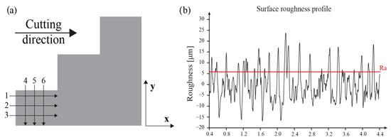
Figure 2.
(a) Measurement directions for the evaluation of bulk workpiece surface roughness (Ra); (b) surface roughness profile and Ra value.
The cutting speed (Vc) and surface roughness (Ra) collected along two orthogonal directions were analysed using the Minitab 19 environment. The statistical question investigates whether the manufacturing process affected Vc and Ra and determines the variables contributing to Vc and Ra variations. Regarding Ra, the study of the effects of the manufacturing process and cutting parameters were analysed separately in the two measurement directions, respectively, for Rax and Ray. Initially, the data were grouped according to the workpiece production process, and then the data were analysed to detect the effect of the investigated factors and their interaction with the Vc and Ra values.
The surfaces of the samples after the cut were also observed with a stereomicroscope, an optical microscope, and SEM.
3. Results and Discussion
Figure 3 compares the surface texture obtained under the same processing condition for each production technology. The surface texture is clearly different among the manufacturing technologies. The surface belonging to the casted sample (Figure 3a) is characterised by small and almost uniform craters. Both the surfaces belonging to the pieces produced by PBF-EB (Figure 3b) and L-PBF (Figure 3c) are characterised by a wave pattern in the wire advancement direction, which could be mainly caused by the periodic inversion of the wire rotation. For the casted sample (Figure 3a,d), the dimensions of the craters are smaller compared to the ones on PBF-EB (Figure 3b,e) and PBF-LB (Figure 3c,f).
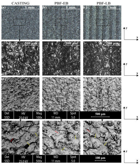
Figure 3.
Surface textures observed with (a–c) microscope and (d–f) SEM on samples produced by (a,d) casting, (b,e) PBF-EB, and (c,f) PBF-LB, machined with the same set of process parameters (ton = 10 s, DC = 8.33%, I = 3 A, workpiece thickness = 20 mm). White arrows indicate examples of spherical debris; red arrows indicate examples of residuals from the wire, while yellow arrows provide an example of craters produced on the workpiece surface by the W-EDM process. The x-axis is parallel to the cut direction.
In addition, the surfaces show a certain quantity of spherical debris (examples are indicated with white arrows), which vary in size and concentration according to the material processing technology. They appear to be smaller in dimensions and number on casted sample surfaces than on PBF-LB or PBF-EB surfaces, where a large amount of the particles is attached to the surface on which the wire inversions took place. This effect is more evident for the PBF-LB sample, in which the craters on the surface are more prominent than in other processes. In fact, the average size of these debris is 14.75 ± 4.02 µm for PBF-LB, 17.73 ± 4.87 µm for PBF-EB, and 12.83 ± 2.13 µm for casting.
The white spherical particles attached to the sample surface (examples are indicated with red arrows) are residual from the electrode, in this case, Molybdenum. The average size of these residual is 3.69 ± 0.69 µm for PBF-LB, 3.30 ± 0.55 µm for PBF-EB, and 3.32 ± 0.72 µm for casting. No significant difference has been detected among the processes.
From the SEM images of the workpiece surface (Figure 3d–f), it is also possible to obtain an indication regarding the craters typically produced by the W-EDM process (examples are indicated by yellow arrows).
Some superficial cracks are also visible, which are caused by high temperature and subsequent rapid cooling.
As an example, analysing the surfaces in Figure 3, the roughness of the surfaces is described by the root mean square value within the cut area, Sq. In this case, the measured value of the entire surface was 8.17 µm for PBF-LB, 4.41 µm for PBF-EB, and 4.60 µm for casting. A strong difference between PBF-LB and the other processes is evident. However, the surfaces show grossly different spatial features, which are revealed by measuring the Rax and Ray (Table 4). Moreover, the more the pattern is evident, as in the case of PBF-LB (Figure 3c), the higher the measured surface roughness is, especially in the wire advancement direction (Rax), as can be observed in Table 4. The pattern can be also noted in the topographies reported in Figure 4.
Table 4.
Surface roughness average and standard deviation values for each direction and material manufacturing technology.
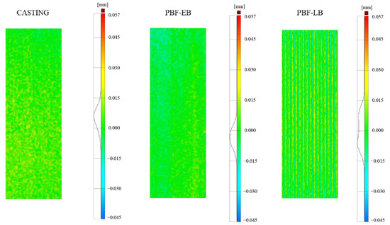
Figure 4.
Surface topography images for samples produced with casting, PBF-EB, and PBF-LB, machined with the same process parameters (ton = 10 s, DC = 8.33%, I = 3 A, workpiece thickness = 20 mm).
This point was confirmed by an ANOVA analysis (Table 5), which highlighted, with a risk level of 0.05, a significant difference between the surface roughness measured in the two directions for PBF-EB and PBF-LB. In addition to the above conclusion, the more the pattern is evident, the more significant the difference between the two values. Since the surface roughness is always higher in the wire advancement direction (Table 4), Rax represents the most critical index for describing the surface finish of the machined surface. For this reason, only Rax is discussed. For completeness, the results concerning Ray are presented in Appendix A.
Table 5.
ANOVA results of surface roughness in the two directions.
As can be observed in Table 4, the cut surface of samples manufactured by the PBF-LB process are more dispersed, and the surfaces are rougher than the corresponding PBF-EB and casted counterparts. In particular, the average value of Rax for the casted workpiece (6.88 µm) was significantly lower than those registered for their PBF-LB and PBF-EB counterparts (9.99 µm and 8.63 µm, respectively). This result indicates the presence of a systematic effect of the material manufacturing technology on the surface roughness. This result is also confirmed by the analysis of variance (ANOVA) in Table 6, which also showed no significant differences for the Vc values using various sample production methods.
Table 6.
ANOVA results for the effect of production technology over cutting speed (Vc) and surface roughness Rax.
Figure 5 shows the main effects of process parameters on Vc and Rax for each technology. In agreement with the previous findings, no significant differences among the technologies can be noticed in the effect of the investigated factors on Vc. An increasing discharge current value causes an increase in the discharge energy and thus, the cutting speed or MRR, in agreement with refs. [7,10,12,29]. A thicker cut determines a lower value of cutting speed. This could be explained by the more considerable amount of material to be removed with the same discharge energy when increasing the thickness, thus causing a cutting speed reduction. Compared to DC, even if ton determines the discharge duration and the productive phase, it does not significantly affect the cutting speed. This could be explained by the multiplicative relationship between the toff and ton, valid for high-speed W-EDM, presented in Equation (2). This relationship implies the presence of high unproductive times (toff) that are always larger than the productive examples. Consequently, DC is low and limits the machine productivity. For this reason, if an increasing erosion rate does not compensate for an increased toff during the productive phase, the unproductive phase becomes the main factor affecting the cutting speed and thus, the process productivity. The effect of toff agrees with that noted in refs. [15,18].
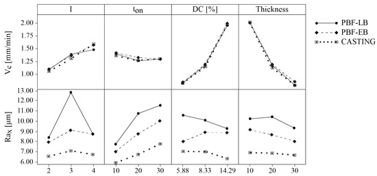
Figure 5.
The main effects of process parameters on cutting speed (Vc) and Rax of all processes.
Regarding surface roughness, contrasting findings can be detected and are peculiar to the material manufacturing process. For the PBF-LB, the increasing discharge current seems to have a quadratic effect on the surface roughness, with a maximum value at 3 A. For PBF-EB instead, only slight Rax variations were observed for currents between 3 A and 4 A. According to Equation (3), an increase in DC and a corresponding reduction of toff produces smoother surfaces in the case of parts produced by PBF-LB. Instead, for parts manufactured by PBF-EB, an increase in DC and thus, a reduction of toff, increases the surface roughness. As noted the literature review, the effect of toff on the final surface roughness is contrasting, and the reasons are unclear. The behaviour of surface roughness in the case of PBF-LB agreed with the results reported by refs. [19,20], in which conventional technologies were used to manufacture the W-EDM machined workpieces. However, the results when machining PBF-EB specimens are corroborated in several works, such as refs. [10,18,21]. For casted samples, similarly to the PBF-LB, the effect of I is almost parabolic, with a maximum at 3A, and an increase in toff* was found detrimental for Rax. Therefore, Despite the same nominal composition, the material behaves as if it were processing different materials [25]. This result may be also explained by the fact that each production technology generates a different thermal history on the material that modifies the material microstructure and the corresponding thermal and electrical conductivities. This effect has been recently demonstrated by Altug et al. [41] when analysing the modification of material properties subjected to different heat treatments. This finding can also be supported by combining the results of Eshkabilov et al. [42] and Strumza et al. [43], which found that the thermal properties of the components are also affected by the material manufacturing technology, and the findings of Han et al. [44] and Choudhuri et al. [45], which demonstrated that the surface morphology strongly depends on the thermal properties of the material. The results presented in these works may also explain the findings of Refs. [46,47], which analysed the surface morphology and topography obtained after W-EDM of a material subjected to different heat treatments. In these works, the authors found that Ra depended on the heat treatment performed on the workpiece.
The cut Thickness and ton variations generate almost the same effect on Rax for both PBF-LB and PBF-EB. The increasing ton has a detrimental impact on Ra in both samples, according to refs. [7,10,12,29]. This could be explained by the fact that an increase in the discharge energy leads to larger and irregularly distributed craters that affect the surface smoothness. On the contrary, since the increased cut thickness causes a reduction in the discharge energy dispersion, Rax decreases, in agreement with the results of Ikram et al. [33].
To determine whether the process parameter variation significantly affects the variation of Vc and Rax in the case of AM parts, an ANOVA was performed with a fixed confidence level equal to 95%. Selecting a p-value threshold equal to 0.05, Table 7 and Table 8 highlight the process parameters and their interaction, which significantly affect the Vc and Ra, respectively.
Table 7.
ANOVA table of process parameters and their interactions for cutting speed Vc in the case of the PBF-LB and PBF-EB processes (significant factors or interactions are highlighted in bold).
Table 8.
ANOVA table of process parameters and their interactions for Rax in the case of the PBF-LB and PBF-EB processes (the significant factors or interactions are highlighted in bold).
For the cutting speed (Table 7), the most significant process parameters are the same for all processes, which confirms the results of Figure 5. The most influential parameter is DC, while all the other process parameters were non-significant. The interactions between I and DC, and I and thickness, even with a total sequential sum of squares below 1%, and DC and thickness were found to be statistically significant. Further statistical tests were performed, removing the non-significant interactions. In this case, thickness and discharge current (I) also significantly affected the cutting speed, while ton remained the only process parameter not to significantly affect the cutting speed. The only significant interaction was found between DC and thickness. Considering these findings, the regression model was determined considering only the DC, I, thickness, and the interaction between DC and thickness.
Regarding Rax, in the case of PBF-LB manufactured parts (Table 8), the discharge current, particularly its quadratic relationship with Rax, is the parameter that affects the surface roughness the most. Thickness and duty factor are non-significant parameters, but their interaction has a significant effect (p-value lower than 0.05). The quadratic impact of thickness had a p-value below 0.05, but its contribution to the overall sum of squares was below 1%; therefore, it was excluded from the significant parameters.
For the sample manufactured by the PBF-EB process (Table 8), the discharge current, DC, and their quadratic relationship with Rax were found to be significant. Moreover, the interaction between DC and discharge current was significant for the roughness variation.
Because of the high contribution to experimental variability of some process parameters (e.g., ton for PBF-EB, Table 8), additional statistical tests were performed for both PBF-LB and PBF-EB, removing the non-significant interactions. These tests showed thickness as a significant factor for both PBF-LB and PBF-EB. Additionally, ton also became significant for PBF-EB. Those parameters were used in the next section to infer the regression models for Rax. The fact that models on surface roughness must be inferred using different inputs demonstrates the remarkable effect of the material manufacturing technologies on the final surface quality after W-EDM cuts.
Regression Models
The regression model that better fits the Vc data for the PBF-LB and PBF-EB process is presented in Equations (5) and (6), respectively.
R2 = 91.27%, R2adj = 90.81% and S = 0.23
R2 = 94.74%, R2adj = 94.47% and S = 0.17
From the remarkably high R2adj and low S values, it is possible to affirm that the adopted models well explain the experimental data. This observation is confirmed by the residual values and their distribution (Figure 6). The positive or negative sign of residuals can be explained by the experimental cutting order, which was always from the smallest to the largest thickness, and could have biased the results. Additionally, certain interactions between process parameters were observed to lead to unstable machining conditions that may have affected the Vc measurements. These instabilities were causal and mainly caused by short circuits, electrode retraction, and poor gap conditions.
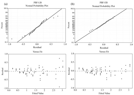
Figure 6.
Residuals plots of the Vc regressions models for (a) PBF-LB and (b) PBF-EB.
Comparing the regression models of Vc determined for parts produced by different AM technologies, it is possible to notice that the difference between the two experimental models is almost negligible because it only consists of a slight variation in the regression coefficients. This fact again underlines that different production technologies do not significantly affect the W-EDM cutting speed index.
The models inferred for Rax reflect the results of ANOVAs. The two equations are characterised by different terms and coefficients (Equations (7) and (8), for PBF-LB and PBF-EB parts, respectively.
R2 = 84.62%, R2adj = 83.15% and S = 1.22
R2 = 74.10%, R2adj = 71.62% and S = 0.92
The high R2 and low S values for both models affirm that the models represent the experimental data well. This observation is confirmed by the distribution of the residuals in Figure 7, where the errors are normally distributed, and no data clustering or sign tendencies have been detected.
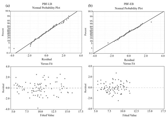
Figure 7.
Residuals plots of the Vc regressions models for (a) PBF-LB and (b) PBF-EB.
4. Conclusions
This paper is the first work that investigates and compares the effect of W-EDM process parameters when processing workpieces produced by different production technologies. A full factorial experimental plan was implemented for each considered technology to test the effect of ton, I, workpiece thickness, and toff or DC. The material production technology strongly affected the Ra after the WED machining of samples. This was found to be particularly evident for DC and discharge current. For PBF-LB parts, increasing DC (lowering toff) is beneficial for Rax, while it is detrimental for the PBF-EB counterpart. In both cases, Rax could be minimised using low I and ton. These results may be explained by differences in microstructure, which may affect the electrical and thermal behaviour of the material. On the contrary, the cutting speed was not influenced by the technology. For this reason, the regression models for estimating the cutting speed for workpieces produced by different AM technologies have no significant differences. Overall, the cutting speed could be increased by adopting high I and high DC values and consequently, low toff values, while larger workpiece thicknesses decreased the cutting speed.
Remarkably, the inferred models presented in this work can be used to predict the Vc and Ra values and to design specific properties for the cut surface, considering the process parameters, production technologies, and sample thickness.
Author Contributions
Conceptualization, M.G., E.A. and F.C.; methodology, M.G.; formal analysis, M.G. and P.A.; investigation, M.G. and P.A.; data curation, P.A.; writing—original draft preparation, P.A.; writing—review and editing, M.G., E.A. and F.C.; visualization, P.A.; supervision, M.G. All authors have read and agreed to the published version of the manuscript.
Funding
This research received no external funding.
Data Availability Statement
The data presented in this study are continued in the manuscript.
Acknowledgments
The authors acknowledge Elena Bassoli and Lucia Denti from Università di Modena e Reggio Emilia for providing the SEM images.
Conflicts of Interest
The authors declare that they have no known competing financial interests or personal relationships that could have appeared to influence the work reported in this paper.
Appendix A
The results of the surface roughness in the y-direction (Ray) for all technologies are summarised in Table 4. It is possible to notice that, as in the case of Rax, there is a significant difference between the three technologies.
This is also highlighted by the ANOVA analysis (Table A1); with a risk level of 0.05, it is possible to affirm that a significant difference between the surface roughness measured in the y-direction could be found for the three different technologies (PBF-LB, PBF-EB, and casting).
Table A1.
ANOVA results of the effect of all process technologies on Ray.
Table A1.
ANOVA results of the effect of all process technologies on Ray.
| Variation Cause | DoF | Variance | F-Ratio | F-Max |
|---|---|---|---|---|
| Examined Factor | 2 | 79.06 | 25.97 | 3.03 |
| Random Errors | 240 | 3.04 | ||
| Total | 242 |
Figure A1 reports the main effects of the investigated factors on Ray. The comparison between the three different technologies showed some differences regarding the effect of some process parameters, but there are not huge differences in the effects on the x-direction. As in the case of Rax, for PBF-LB and casting, the discharge current seems to have a quadratic effect on the surface roughness along the y-direction, even if this effect is less marked in the latter case. For PBF-EB, increasing the discharge current has a detrimental effect on Ray, but with linear dependence. Among the three technologies, the ton and thickness increase have approximately the same effect on Ray.
Similarly to Rax, ton causes a surface roughness increment because the increase in the discharge energy leads to larger and more irregularly distributed craters that affect the surface smoothness. The thickness causes a surface roughness reduction due to the reduction in the discharge energy dispersion. As for Rax, increasing DC (reducing the toff value) was found to have a detrimental effect on Ray for PBF-EB, while it was found to lower the surface roughness in the case of PBF-LB and casting. For all process parameter effects, the considerations made in paragraph 3 for additively manufactured and casted replicas are still valid, in this case.

Figure A1.
Main effects of process parameters Ray of all processes.
Figure A1.
Main effects of process parameters Ray of all processes.

Similarly to Rax, the analysis of variance (ANOVA) was performed with a fixed confidence level equal to 95% to determine which process parameters and interactions significantly affect Ray variation for the two AM processes. Table A2 reports all the process parameters and interactions found significant for PBF-LB and PBF-EB. In both cases, a key role is played by ton and DC, which are the two most significant factors, while the significance of the other parameters and interactions varies depending on the production technology.
Table A2.
ANOVA table of significant process parameters and interactions for Ray for PBF-LB and PBF-EB.
Table A2.
ANOVA table of significant process parameters and interactions for Ray for PBF-LB and PBF-EB.
| PBF-LB | PBF-EB | ||||||||
|---|---|---|---|---|---|---|---|---|---|
| Source | DF | Adj. SS | Adj. MS | p-Value | Source | DF | Adj. SS | Adj. MS | p-Value |
| Regression | 6 | 277.20 | 46.20 | 0.000 | Regression | 5 | 168.36 | 33.67 | 0.000 |
| I | 1 | 18.87 | 18.87 | 0.000 | I | 1 | 7.13 | 7.13 | 0.003 |
| ton | 1 | 20.36 | 20.36 | 0.000 | ton | 1 | 123.28 | 123.28 | 0.000 |
| DC | 1 | 23.45 | 23.45 | 0.000 | DC | 1 | 12.71 | 12.71 | 0.000 |
| Thickness | 1 | 14.41 | 14.42 | 0.000 | Thickness | 1 | 11.32 | 11.32 | 0.000 |
| I × I | 1 | 17.76 | 17.75 | 0.000 | I × DC | 1 | 17.52 | 17.52 | 0.000 |
| ton × ton | 1 | 6.01 | 6.01 | 0.017 | |||||
| Error | 74 | 74.79 | 1.01 | Error | 75 | 56.29 | 0.75 | ||
| Total | 80 | Total | 80 | ||||||
Based on ANOVA results, two regression models, one for each additive technology, were determined as a function of the significant process parameters and interactions. In Equations (A1) and (A2), for PBF-LB and PBF-EB, respectively. In addition, R2, R2adj and S are reported as well. According to the values and the residual values and distribution (Figure A2a,b), for which the errors are normally distributed and no data clustering or sign tendencies have been detected, it is possible to affirm that both models well explain the experimental data.
R2 = 78.75%, R2adj = 77.03% and S = 1.00
R2 = 74.94%, R2adj = 73.27% and S = 0.86
The high R2 and low S values for both models affirm that the models represent the experimental data well. This observation is confirmed by the distribution of the residuals in Figure 7, where the errors are normally distributed, and no data clustering or sign tendencies have been detected.

Figure A2.
Residuals plots of the Rax regressions models for (a) PBF-LB and (b) PBF-EB.
Figure A2.
Residuals plots of the Rax regressions models for (a) PBF-LB and (b) PBF-EB.

References
- Ho, K.H.; Newman, S.T.; Rahimifard, S.; Allen, R.D. State of the art in wire electrical discharge machining (WEDM). Int. J. Mach. Tools Manuf. 2004, 44, 1247–1259. [Google Scholar] [CrossRef]
- Kunieda, M.; Lauwers, B.; Rajurkar, K.P.; Schumacher, B.M. Advancing EDM through Fundamental Insight into the Process. CIRP Ann. 2005, 54, 64–87. [Google Scholar] [CrossRef]
- Garg, R.K.; Singh, K.K.; Sachdeva, A.; Sharma, V.S.; Ojha, K.; Singh, S. Review of research work in sinking EDM and WEDM on metal matrix composite materials. Int. J. Adv. Manuf. Technol. 2010, 50, 611–624. [Google Scholar] [CrossRef]
- Defanti, S.; Denti, L.; Vincenzi, N.; Gatto, A. Preliminary assessment of electro-chemical machining for aluminum parts produced by laser-based powder bed fusion. Smart Sustain. Manuf. Syst. 2020, 4, 121–134. [Google Scholar] [CrossRef]
- Abhilash, P.M.; Chakradhar, D. Sustainability improvement of WEDM process by analysing and classifying wire rupture using kernel-based naive Bayes classifier. J. Braz. Soc. Mech. Sci. Eng. 2021, 43, 1–9. [Google Scholar] [CrossRef]
- Rao, P.S.; Ramji, K.; Satyanarayana, B. Experimental Investigation and Optimization of Wire EDM Parameters for Surface Roughness, MRR and White Layer in Machining of Aluminium Alloy. Procedia Mater. Sci. 2014, 5, 2197–2206. [Google Scholar] [CrossRef]
- Kumar, A.; Kumar, V.; Kumar, J. Multi-response optimization of process parameters based on response surface methodology for pure titanium using WEDM process. Int. J. Adv. Manuf. Technol. 2013, 68, 2645–2668. [Google Scholar] [CrossRef]
- Ghodsiyeh, D.; Lahiji, M.A.; Ghanbari, M.; Shirdar, M.R.; Golshan, A. Optimizing material removal rate (MRR) in WEDMing titanium alloy (Ti6Al4V) using the taguchi method. Res. J. Appl. Sci. Eng. Technol. 2012, 4, 3154–3161. [Google Scholar]
- Tosun, N.; Cogun, C.; Inan, A. The effect of cutting parameters on workpiece surface roughness in wire EDM. Mach. Sci. Technol. 2003, 7, 209–219. [Google Scholar] [CrossRef]
- Dabade, U.A.; Karidkar, S.S. Analysis of Response Variables in WEDM of Inconel 718 Using Taguchi Technique. Procedia Cirp 2016, 41, 886–891. [Google Scholar] [CrossRef]
- Venkatarao, K.; Anup Kumar, T. An experimental parametric analysis on performance characteristics in wire electric discharge machining of Inconel 718. Proc. Inst. Mech. Eng. Part C J. Mech. Eng. Sci. 2019, 14, 4836–4849. [Google Scholar] [CrossRef]
- Rao, K.V.; Raju, L.R.; Kumar, C.K. Modeling of kerf width and surface roughness in wire cut electric discharge machining of Ti-6Al-4V. Proc. Inst. Mech. Eng. Part E J. Process. Mech. Eng. 2020, 234, 533–542. [Google Scholar] [CrossRef]
- Nain, S.S.; Garg, D.; Kumar, S. Evaluation and analysis of cutting speed, wire wear ratio, and dimensional deviation of wire electric discharge machining of super alloy Udimet-L605 using support vector machine and grey relational analysis. Adv. Manuf. 2018, 6, 225–246. [Google Scholar] [CrossRef]
- Devarajaiah, D.; Muthumari, C. Evaluation of power consumption and MRR in WEDM of Ti–6Al–4V alloy and its simultaneous optimization for sustainable production. J. Braz. Soc. Mech. Sci. Eng. 2018, 40, 1–18. [Google Scholar] [CrossRef]
- Singh, T.; Misra, J.P.; Singh, B. Experimental Investigation of Influence of Process Parameters on MRR during WEDM of Al6063 alloy. Mater. Today Proc. 2017, 4, 2242–2247. [Google Scholar] [CrossRef]
- Singh, H.; Garg, R. Effects of process parameters on material removal rate in WEDM. J. Achiev. Mater. Manuf. Eng. 2009, 32, 70–74. [Google Scholar]
- Sharma, N.; Khanna, R.; Gupta, R. Multi Quality Characteristics of WEDM Process Parameters with RSM. Procedia Eng. 2013, 64, 710–719. [Google Scholar] [CrossRef]
- Chalisgaonkar, R.; Kumar, J. Optimization of WEDM process of pure titanium with multiple performance characteristics using Taguchi’s DOE approach and utility concept. Front. Mech. Eng. 2013, 8, 201–214. [Google Scholar] [CrossRef]
- Poros, D.; Wisniewska, M.; Zaborski, S. Comparative analysis of wedm with different wire electrodes applied to cut titanium ti6al4v. J. Mach. Eng. 2020, 20, 116–125. [Google Scholar] [CrossRef]
- Priyankara, K.P.M.; Perera, G.I.P. Experimental Investigation to Achieve Minimum Surface Roughness in Wire EDM Process. In ICSBE 2018: Proceedings of the 9th International Conference on Sustainable Built Environment; Springer: Singapore, 2020; pp. 239–251. [Google Scholar]
- Sharma, P.; Chakradhar, D.; Narendranath, S. Evaluation of WEDM performance characteristics of Inconel 706 for turbine disk application. Mater. Des. 2015, 88, 558–566. [Google Scholar] [CrossRef]
- Kumar, A.; Kumar, V.; Kumar, J. Experimental investigation on material transfer mechanism in wedm of pure titanium (Grade-2). Adv. Mater. Sci. Eng. 2013, 2013, 847876. [Google Scholar] [CrossRef]
- kumar, S.; Khan, M.A.; Muralidharan, B. Processing of titanium-based human implant material using wire EDM. Mater. Manuf. Process. 2019, 34, 695–700. [Google Scholar] [CrossRef]
- Sen, R.; Choudhuri, B.; Barma, J.D.; Chakraborti, P. Study the impact of process parameters and electrode material on wire electric discharge machining performances. Mater. Today Proc. 2018, 5, 7552–7560. [Google Scholar] [CrossRef]
- Calvo, R.; Daniel, M. Wire electrical discharge machining (EDM) setup parameters influence in functional surface roughness. Procedia Manuf. 2019, 41, 602–609. [Google Scholar] [CrossRef]
- Durairaj, M.; Sudharsun, D.; Swamynathan, N. Analysis of process parameters in wire EDM with stainless steel using single objective Taguchi method and multi objective grey relational grade. Procedia Eng. 2013, 64, 868–877. [Google Scholar] [CrossRef]
- Tosun, N.; Cogun, C.; Tosun, G. A study on kerf and material removal rate in wire electrical discharge machining based on Taguchi method. J. Mater. Process. Technol. 2004, 152, 316–322. [Google Scholar] [CrossRef]
- Mahapatra, S.S.; Patnaik, A. Optimization of wire electrical discharge machining (WEDM) process parameters using Taguchi method. Int. J. Adv. Manuf. Technol. 2007, 34, 911–925. [Google Scholar] [CrossRef]
- Tosun, N. The effect of the cutting parameters on performance of WEDM. KSME Int. J. 2003, 17, 816–824. [Google Scholar] [CrossRef]
- Kumar, A.; Kumar, U.A.; Laxminarayana, P. Optimization of surface roughness and kerf width by wire cut-electrical discharge machining on inconel 625. Mater. Today Proc. 2020, 27, 1460–1465. [Google Scholar] [CrossRef]
- Gamage, J.R.; DeSilva, A.K.M.; Chantzis, D.; Antar, M. Sustainable machining: Process energy optimisation of wire electrodischarge machining of Inconel and titanium superalloys. J. Clean Prod. 2017, 164, 642–651. [Google Scholar] [CrossRef]
- Kumar, A.; Kumar, V.; Kumar, J. Parametric Effect on Wire Breakage Frequency and Surface Topography in WEDM of Pure Titanium. J. Mech. Eng. Technol. 2013, 1, 51–56. [Google Scholar] [CrossRef]
- Ikram, A.; Mufti, N.A.; Saleem, M.Q.; Khan, A.R. Parametric optimization for surface roughness, kerf and MRR in wire electrical discharge machining (WEDM) using Taguchi design of experiment. J. Mech. Sci. Technol. 2013, 27, 2133–2141. [Google Scholar] [CrossRef]
- Vaidyaa, P.; John, J.J.; Puviyarasan, M.; Prabhu, T.R.; Prasad, N.E. Wire EDM Parameter Optimization of AlSi10Mg Alloy. Trans. Indian Inst. Met. 2021, 74, 2869–2885. [Google Scholar] [CrossRef]
- Franczyk, E.; Machno, M.; Zębala, W. Investigation and optimization of the slm and wedm processes’ parameters for the AlSi10Mg-sintered part. Materials 2021, 14, 410. [Google Scholar] [CrossRef] [PubMed]
- Calignano, F.; Manfredi, D.; Ambrosio, E.P.; Biamino, S.; Pavese, M.; Fino, P. Direct fabrication of joints based on direct metal laser sintering in aluminum and titanium alloys. Procedia CIRP 2014, 21, 129–132. [Google Scholar] [CrossRef]
- Galati, M.; Rizza, G.; Defanti, S.; Denti, L. Surface roughness prediction model for Electron Beam Melting (EBM) processing Ti6Al4V. Precis. Eng. 2021, 69, 19–28. [Google Scholar] [CrossRef]
- Kumar, S.; Singh, R.; Singh, T.P.; Sethi, B.L. Surface modification by electrical discharge machining: A review. J. Mater. Process. Technol. 2009, 209, 3675–3687. [Google Scholar] [CrossRef]
- ISO 4288; 1996-Geometrical Product Specifications (GPS)—Surface Texture: Profile Method—Rules and Procedures for the Assessment of Surface Texture. International Organization for Standardization: Geneva, Switzerland, 1996.
- Calignano, F. Investigation of the accuracy and roughness in the laser powder bed fusion process. Virtual Phys. Prototyp. 2018, 13, 97–104. [Google Scholar] [CrossRef]
- Altug, M.; Erdem, M.; Ozay, C. Experimental investigation of kerf of Ti6Al4V exposed to different heat treatment processes in WEDM and optimization of parameters using genetic algorithm. Int. J. Adv. Manuf. Technol. 2015, 78, 1573–1583. [Google Scholar] [CrossRef]
- Eshkabilov, S.; Ara, I.; Sevostianov, I.; Azarmi, F.; Tangpong, X. Mechanical and thermal properties of stainless steel parts, manufactured by various technologies, in relation to their microstructure. Int. J. Eng. Sci. 2021, 159, 103398. [Google Scholar] [CrossRef]
- Strumza, E.; Yeheskel, O.; Hayun, S. The effect of texture on the anisotropy of thermophysical properties of additively manufactured AlSi10Mg. Addit. Manuf. 2019, 29, 100762. [Google Scholar] [CrossRef]
- Han, F.; Jiang, J.; Yu, D. Influence of machining parameters on surface roughness in finish cut of WEDM. Int. J. Adv. Manuf. Technol. 2007, 34, 538–546. [Google Scholar] [CrossRef]
- Choudhuri, B.; Sen, R.; Ghosh, S.K.; Saha, S.C. Comparative machinability characterization of wire electrical discharge machining on different specialized AISI steels. Bull. Mater. Sci. 2020, 43, 1–12. [Google Scholar] [CrossRef]
- Mouralova, K.; Kovar, J.; Klakurkova, L.; Blazik, P.; Kalivoda, M.; Kousal, P. Analysis of surface and subsurface layers after WEDM for Ti-6Al-4V with heat treatment. Measurement 2018, 116, 556–564. [Google Scholar] [CrossRef]
- Mouralova, K.; Kovar, J.; Klakurkova, L.; Prokes, T.; Horynova, M. Comparison of morphology and topography of surfaces of WEDM machined structural materials. Measurement 2017, 104, 12–20. [Google Scholar] [CrossRef]


Disclaimer/Publisher’s Note: The statements, opinions and data contained in all publications are solely those of the individual author(s) and contributor(s) and not of MDPI and/or the editor(s). MDPI and/or the editor(s) disclaim responsibility for any injury to people or property resulting from any ideas, methods, instructions or products referred to in the content. |
© 2023 by the authors. Licensee MDPI, Basel, Switzerland. This article is an open access article distributed under the terms and conditions of the Creative Commons Attribution (CC BY) license (https://creativecommons.org/licenses/by/4.0/).