Article

Carbon Nanotube–Carbon Nanocoil Hybrid Film Decorated by Amorphous Silicon as Anodes for Lithium-Ion Batteries

by
Huan Chen
1,
Chen Wang
2,
Zeng Fan
3,
Chuanhui Cheng
3,
Liang Hao
4,* and
Lujun Pan
3,*
1
School of Integrated Circuits, Dalian University of Technology, Dalian 116024, China
2
State Key Laboratory of ASIC and Systems, School of Microelectronics, Fudan University, Shanghai 200433, China
3
School of Physics, Dalian University of Technology, Dalian 116024, China
4
Shanghai Key Laboratory of Multiphase Flow and Heat Transfer in Power Engineering, School of Energy and Power Engineering, University of Shanghai for Science and Technology, Shanghai 200093, China
*
Authors to whom correspondence should be addressed.
J. Compos. Sci. 2024, 8(9), 350; https://doi.org/10.3390/jcs8090350
Submission received: 15 August 2024 / Revised: 30 August 2024 / Accepted: 4 September 2024 / Published: 6 September 2024
(This article belongs to the Special Issue Recent Progress in Hybrid Composites)

Abstract

:
Silicon (Si) as the anode material for lithium-ion batteries (LIBs) has attracted much attention due to its high theoretical specific capacity (4200 mAh/g). However, the specific capacity and cycle stability of the LIBs are reduced due to the pulverization caused by the expansion of Si coated on Cu (copper) foil during cycles. In order to solve this problem, researchers have used an ultra-thin Si deposition layer as the electrode, which improves cyclic stability and obtains high initial coulomb efficiency of LIBs. However, suitable substrate selection is crucial to fabricate an ultrathin Si deposition layer electrode with excellent performance, and a substrate with a three-dimensional porous structure is desirable to ensure the deposition of an ultrathin Si layer on the whole surface of the substrate. In this paper, the Si thin layer has been deposited on a binder-free hybrid film of carbon nanotubes (CNTs) and carbon nanocoils (CNCs) by magnetron sputtering. Compared with densely packed CNT film and flat Cu foil, the loose and porous film provides a large surface area and space for Si deposition, and Si can be deposited not only on the surface but also in the interior part of the film. The film provides a large number of channels for the diffusion and transmission of Li+, resulting in the rapid diffusion rate of Li+, which improves the effective lithium storage utilization of Si. Furthermore, the CNC itself is super elastic, and film provides an elastic skeleton for the Si deposition layer, which eases its volume expansion during charge and discharge processes. Electrochemical tests have showed that the Si/CNT–CNC film electrode has excellent performance as anode for LIBs. After 200 cycles, the Si/CNT–CNC film electrode still had possessed a specific capacity of 2500 mAh/g, a capacity retention of 92.8% and a coulomb efficiency of 99%. This paper provides an effective way to fabricate high performance Si-nanocarbon composite electrodes for LIBs.

1. Introduction

Due to the massive use of fossil fuels, the problems of energy shortages and environment destruction have become increasingly serious. However, the emergence of new energy sources has alleviated this problem. Lithium-ion batteries (LIBs) are an important part of new energy technologies, and obtaining high-performance LIBs is particularly crucial for the development of new energy sources [1,2]. As anode materials for LIBs, they have a great effect on achieving optimal power and energy densities. The current commercial anode is graphite, which has a relatively low specific capacity (372 mAh/g) and is difficult to use for the application of fast-charging batteries due to the slow kinetics and lithium plating [3,4]. Silicon (Si), having a high theoretical capacity (4200 mAh/g), has become a new research hotspot for anode materials [5]. Compared to graphite, Si has a low working potential (0.25 V vs. Li/Li+) and 10 times the capacity [6,7]. In addition, Si has the excellent characteristics of low-cost, abundant resources, environmentally friendliness, and outstanding reversible capacity, making it particularly attractive to use for LIBs [8]. However, the huge volume expansion (more than 300%), low conductivity and insufficient utilization of Si, which can rapidly decrease its electrochemical performance causing electrode cracking and decreased specific capacity, are great hindrances for the further application of Si [9,10,11,12,13]. In order to solve the above problems, extensive studies have been conducted on Si anodes: (1) Modifying the characteristics of Si, including designing structures of the Si and reducing the Si size down to the micro/nanoscale [14,15,16] and (2) reducing the thickness of the Si deposition layer above the substrate [17,18,19,20]. Increasing the porosity and conductivity of the Si-based composites can provide a large deposition area and space to improve the utilization rate of Si and while also enhancing rapid electron and ion transportation. Xie et al. proposed and successfully prepared yolk shell Si@C@void@C nanohybrids, which dramatically improved the Li+/electron conductivity and the buffering of the huge volume variation of Si [21]. Chockla et al. reported a nonwoven fabric composed of Si nanowires. The polyphenylsilane coating attached to the surface of the nanofabric was converted to a carbonaceous layer by thermal annealing in a reducing environment, which significantly increased the electrical conductivity of the material. The mechanically flexible property also moderated the volume expansion of the silicon. The self-supporting Si nanowire fabric as an anode shows excellent cycling performance and high energy storage for LIBs [22]. Furthermore, the improvement of cycling stability is obtained by reducing the size of Si, e.g., Si nanoparticles, nanowires, nanotubes and thin films [23,24,25,26,27]. Particularly, the Si thin film is an appealing anode material for LIBs due to its advantage of simple synthesis. Currently, extensive research efforts have been devoted to the thickness of the Si thin film, which has a significant impact on the performance of LIBs [28,29,30]. The magnetron sputtering technique has been widely employed for preparing thin films due to the advantages of simple fabrication process, wide deposition range, large coating area and strong film adhesion to the substrate [31,32,33]. Tocoglu et al. deposited a thin amorphous Si deposition layer on graphene/carbon nanotube (CNT) flexible composite anodes via a radio frequency (RF) magnetron sputtering method, which contributed to the capacity enhancement of LIBs [34]. Tong et al. prepared a binder-free multiply sandwiched Si/carbon thin film electrode by the magnetron sputtering technique. The electrochemical performance of LIBs using this electrode have been enhanced by designing a rational structure, which showed a high reversible specific capacity of 1300 mAh/g and a capacity retention of 90.1% after 200 cycles [35]. However, the severe capacity loss in the first cycle and the surface corrosion and passivation of the Si in electrolytes restrict further capacity enhancement of Si-based LIBs for high-mass-loading anodes [36,37,38]. Therefore, more studies are still necessary to further construct high performance Si-based LIBs.
In addition, a lot of research has been invested in silicon/carbon (Si/C) composite materials by combining high-capacity Si and different dimensions of carbon materials to achieve the excellent performance of LIBs. For example, one-dimensional carbon materials, including CNTs [39] and carbon nanofibers, were adopted to increase the uniform deposition of Si on their surfaces and improve the transport of electrons and lithium ions [40]. Two-dimensional graphene sheets were also used to provide more contact sites for Si, thus achieving the uniform distribution of Si and high conductivity of the overall electrode. Si nanoparticles were further coated with carbon shells to form a stable SEI film on the surface and to mitigate the expansion and contraction of Si [41]. Since carbon materials have so many excellent properties, they are preferred as raw materials when considering the Si sputtering substrate in this paper.
Three-dimensional (3D) porous substrate surface structure can provide sufficient space for Si deposition to increase effective Si loading as well as the cycle life of a thin film Si electrode. Our previous experiments have proved that the addition of carbon nanocoils (CNCs) prevents the clumping of CNTs and maximizes their usable surface area, resulting in the loose and porous surface structure of the hybrid film [42,43]. In this paper, magnetron sputtering technology is used to directly sputter Si on a CNT film, a CNT–CNC film and a copper (Cu) foil. The CNT film, the CNT–CNC film and the Cu foil are regarded as current collectors (CCs) in the electrodes. Compared with densely packed CNT film and flat Cu foil, the CNT–CNC film provides a large effective surface area and space for Si deposition, and Si can be deposited not only on the surface but also in the interior part of the film. Moreover, the CNT–CNC film provides channels for the diffusion and transmission of Li+, resulting in the rapid diffusion rate of Li+, and improves the effective lithium storage utilization of the Si. In addition, the CNC itself is super elastic, and the CNT–CNC film provides an elastic skeleton for the Si deposition layer, which eases its volume expansion during charge and discharge processes. At the end of the 200th cycle, the Si/CNT–CNC film electrode still had possessed a specific capacity of 2500 mAh/g, a capacity retention of 92.8% and a coulomb efficiency of 99%.
It is worth emphasizing that compared with published papers, the novel features of the method in this paper are as follows: Firstly, the CNT–CNC film forms an elastic conductive network and has a large number of pores due to the addition of CNCs, which not only improves the conductivity of the overall electrode, but also provides enough space for the expansion and contraction of Si to buffer the drastic changes in volume, making the electrode structure more stable. Secondly, the application of magnetron sputtering enables the Si to be directionally deposited at a large depth through pores, so the Si deposition layer on the surface of the Si/CNT–CNC film is the thinnest, which is crucial for the formation of stable SEI film during the first discharge. In contrast, the Si deposition layer on the surface of the Si/CNT film is thick and has higher Si exposure. The resulting Si particle crushing and continuous SEI formation would consume Si, leading to capacity attenuation. Therefore, this paper provides a new choice for a suitable Si sputtering substrate.

2. Materials and Methods

2.1. The Synthesis of CNCs

We synthesized CNCs using the method of chemical vapor deposition [44,45]. The fabrication process is as follows: First, the catalyst solution is a mixture of ethanol and the α-Fe2O3/SnO2 nanocomposites, and the mixture requires sufficient ultrasonic time for full contact (30 min). Then, using the Al2O3 substrate, the catalyst solution was dripped onto it by pipette and the treated substrate was dried. At last, CNCs were prepared by placing the treated substrate in a tube furnace and introducing acetylene in an atmospheric pressure system.

2.2. The Synthesis of CNT Film and CNT–CNC Film

The complete preparation of CNT film and CNT–CNC film had been described in detail in previous work [42,43,46]. Taking the CNT–CNC film as an example, the following content is a brief description of the experimental process: Firstly, the acidified CNTs and CNCs were thoroughly mixed with deionized water in a ratio of 1:1. Secondly, the uniformly dispersed solution was obtained by ultrasonic treatment. Finally, a self-supporting CNT–CNC film was prepared by using a vacuum filter.

2.3. Electrode Fabrications

The electrodes after sputtering treatment are respectively named Si/CNT film electrode, Si/CNT–CNC film electrode and Si/Cu electrode, which are directly used as the anodes for LIBs. Si thin layers were deposited on the surface of different substrates by using a FJL560III-type magnetron sputtering machine (Chinese Academy of Sciences Shenyang Scientific Instrument Co., Ltd., Shenyang, China), and p-type amorphous Si (purity 99.999%) was used as the sputtering target. The alternating sputtering of Si was carried out by radio frequency (RF) with a vacuum pressure of 5 × 10⁻⁴ Pa. The sputtering process was completed at room temperature and the working pressure of 1.5 Pa was obtained by injecting 30 sccm argon gas (purity 99.999%). Before the formal sputtering, it is necessary to pre-sputter for 5 min, which is conducted to remove impurities on the surface of the target.

2.4. Electrode Characterization and Cell Measurement

The surface and cross-section morphologies of the prepared electrodes were observed using field-emission scanning electron microscopy (FE-SEM, NOVA NanoSEM 450 FEI, Hillsboro, OR, USA and JSM-7610F Plus, JEOL, Tokyo, Japan) and energy dispersive X-ray spectroscopy (EDS). Raman spectroscopy (Finder 930, Beijing Zolix Instrument Co., Ltd., Beijing, China) was generated by using a laser source with a wavelength of 532 nm to detect the characteristic peaks of the material.
With the Si/CNT film electrode, the Si/CNT–CNC film electrode and the Si/Cu electrode as the anodes and lithium foil as the reference electrode, a polyethylene separator (2400, Celgard, Charlotte, NC, USA) was placed in the middle of the cathode and anode to fabricate coin-type (CR2032) cells in glovebox filled with argon. The electrolyte used in the preparation process was a LiPF6 solution (1 M), in which the solvent was composed of ethyl carbonate (EC), methyl carbonate (EMC) and dimethyl carbonate (DMC) mixed with a mass ratio of 1:1:1.
The galvanostatic charge/discharge process was investigated between 0.01 and 2.00 V with the use of a LANHE CT2001A battery tester (Wuhan LAND Electronic Co., Ltd., Wuhan, China) at room temperature. The electrochemical workstation (CHI 760E) was used to measure the electrochemical impedance spectrum (EIS) and the cyclic voltammetry (CV).

3. Results

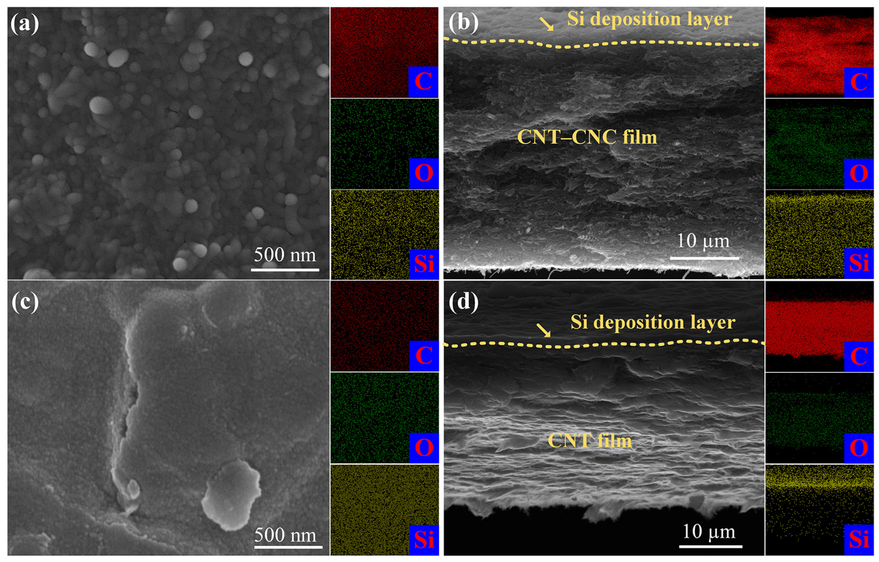
3.1. Characterization of the Film and Electrode

As mentioned in the experimental procedures, various thicknesses of the Si deposition layer were deposited on CNT films to fabricate the Si/CNT film electrodes at different RF powers (50 W, 75 W, 150 W). The surface and cross-section morphologies of the Si/CNT film electrodes are represented in Figure S1. As shown in Figure S1a, at the sputtering power of 50 W, the shape of the CNTs is clearly visible and it is evident that Si deposition results in increasing the diameter of CNTs at the expense of porosity between the interchannels of CNTs. The average tube diameter of the Si coated CNTs is in the range of 40–60 nm, while the diameter of raw CNTs is 8–15 nm. It can be seen from Figure S1b that the surface of the CNT film is only covered by a thin Si deposition layer with a thickness of about 100 nm. When the sputtering power is increased to 75 W, as can be seen from Figure S1c,d, the CNT film has been completely covered by the Si deposition layer with a thickness of about 700 nm. As depicted in Figure S1e,f, when the sputtering power continues up to 150 W, the sputtered Si deposition layer on the surface of the CNT film has accumulated in layers. It can be seen from the cross-sectional image that the thickness of the Si deposition layer significantly increases to about 1300 nm, and there are obvious cracks between the Si deposition layer and the CNT film. Thus, with the increase of sputtering power, the thickness of the Si deposition layer increases significantly.
The electrochemical characterization of the Si/CNT film electrodes at different sputtering powers have been examined first. The specific capacity of the charge/discharge process is calculated according to the mass of Si. Figure S2 shows the working state of the electrode under different sputtering powers. The highest discharge capacity and the best cycle performance are obtained by using the Si/CNT film electrode at the sputtering power of 75 W. At the 100th cycle, the specific capacity of this cell is about 1100 mAh/g at a specific current of 50 mA/g between 0.01 and 2.00 V vs. Li/Li+, but it is only 426 mAh/g for the Si/CNT film electrode at the sputtering power of 50 W. In addition, the coin cell of the Si/CNT film electrode with a sputtering power of 150 W can only be tested to the 40th cycle. As a result, when the sputtering power is 50 W, the Si deposition layer is thinner, the Si content is less, and the specific capacity of the LIBs is low. When the sputtering power is 150 W, the Si deposition layer is thicker, the Si content is larger, and the interaction force between the Si deposition layer and the CNT film is reduced, so there are a large number of cracks at the interface between the Si deposition layer and the CNT film, which is obviously adverse to the performance of LIBs. Therefore, choosing a suitable sputtering power is crucial to obtain the excellent performance of LIBs, and 75 W is finally determined to be the best sputtering power.
As mentioned above, the thickness of Si deposition layer enlarges with the increase of sputtering power. However, the increased thickness of the Si deposition layer seriously reduces the effective utilization rate of Si in the Si/CNT film electrode. Therefore, the method of using the different sputtering substrates is adopted to obtain a homogenous Si deposition layer and thus improve the utilization rate of Si. Hence, in this work, the CNT film, the CNT–CNC film and the Cu foil are used as CCs for comparison at the sputtering power of 75 W. The morphology of the Si deposition layer sputtered on different CC surfaces is different. Because the surface of the CNT film is dense, the accumulated Si deposition layer on its surface is thick and a small amount of Si can enter the interior, while the CNT–CNC film provides enough space for a lot of Si longitudinal deposition due to its porous surface structure. As a traditional CC, the surface of the Cu foil is rough, and the Si deposition layer can only accumulate on its surface. Subsequently, SEM is used to visualize the surface morphology of the Si deposition layer and the interfacial morphology between the different CCs and the Si deposition layer after sputtering. The image exhibited in Figure 1a shows that the raw CNT film represents a dense arrangement with only a few holes, while the sputtered CNT film demonstrates that the Si deposition layer completely covers the CNT film in Figure 1b,c. Meanwhile, it is known from Figure 1d that the Si deposition layer with the thickness of 700 nm closely contacts the CNT film. Then, when the CNT–CNC film is sputtered as a CC, according to Figure 1e, before sputtering there are sufficient holes on the surface of the CNT–CNC film by the addition of CNCs. After sputtering, as it can be seen from Figure 1f,g, the surface of the CNT–CNC film is covered by a thin Si deposition layer, while the CNCs on the surface are still clearly visible. As it can be seen from Figure 1h, the thickness of the Si deposition layer on the surface of the CNT–CNC film is only about 280 nm, indicating that the Si is deposited internally through holes on the surface of the CNT–CNC film, resulting in improving the utilization of the Si. Further, as for the Cu foil that is sputtered as a CC, it is clear from Figure 1i that before sputtering the surface of the Cu foil is packed with large particles. After sputtering, as it can be seen from Figure 1j,k, the Si deposition layer is very thick and the growth of the Si deposition layer is according to the morphology of the Cu foil surface. In addition, the thickness of the Si deposition layer on the surface of the Cu foil is 5000 nm, and it can be concluded that the different CC results in the different surface morphology and thickness of the Si deposition layer. The reasons for this result are as follows: The surface of the Cu foil has no holes, and the surface of the CNT film is as dense as a net, having fewer holes. However, in the CNT–CNC film, there are a large number of holes on the surface due to the presence of the CNCs. Therefore, when the Si is deposited on the surface of the CNT–CNC film, it can enter the interior through the large holes easily, so under the same deposition conditions of the Si, the Si deposition layer on the surface of the CNT–CNC film is the thinnest.
In order to further investigate the reason for the thinnest deposition thickness of the Si/CNT–CNC film electrode, SEM has been used to visualize the surface and cross-section morphology. As it can be seen obviously from the EDS distribution of elements in Figure 2a,b, the Si layer was deposited homogenously on the surface of the CNT–CNC film. From the view of the cross-section, a thin Si deposition layer is obviously aggregated at the contact interface between the Si deposition layer and the CNT–CNC film, and a lot of the Si is penetrated deeply into the interior of the CNT–CNC film from top to bottom due to its porous and loose structure. In contrast, as shown in Figure 2c,d, the surface of the Si/CNT film is stacked with a very thick Si deposition layer. It can be seen from the cross-section image that due to the compact arrangement of the CNTs on the surface of the CNT film, a thick Si deposition layer exists at the contact interface between the Si deposition layer and the CNT film. This is why the Si/CNT–CNC film has the thinnest layer of the Si deposition layer on its surface.
Raman spectroscopy analysis results are shown in Figure S3. The G band representing the degree of graphitization of the material appears at 1580 cm−1 for the Si/CNT film and Si/CNT–CNC film electrodes, while the D band related to structural defects is observed at 1350 cm−1. Compared to the raw CNT film and the CNT–CNC film, the band of sputtered electrodes with different Si deposition layer thicknesses shows at 500 cm−1, which corresponds to the TO (transverse optic) frequencies [17]. The crystalline band Si was not detected, which fully indicates that the Si deposition layer is amorphous. In addition, the D and G bands become weaker after sputtering, which is due to the fact that the CNT film and the CNT–CNC film are completely covered by the Si deposition layer. It is worth mentioning that the lowest peak strength of the Si/CNT–CNC film also shows that the surface Si deposition layer is the thinnest.

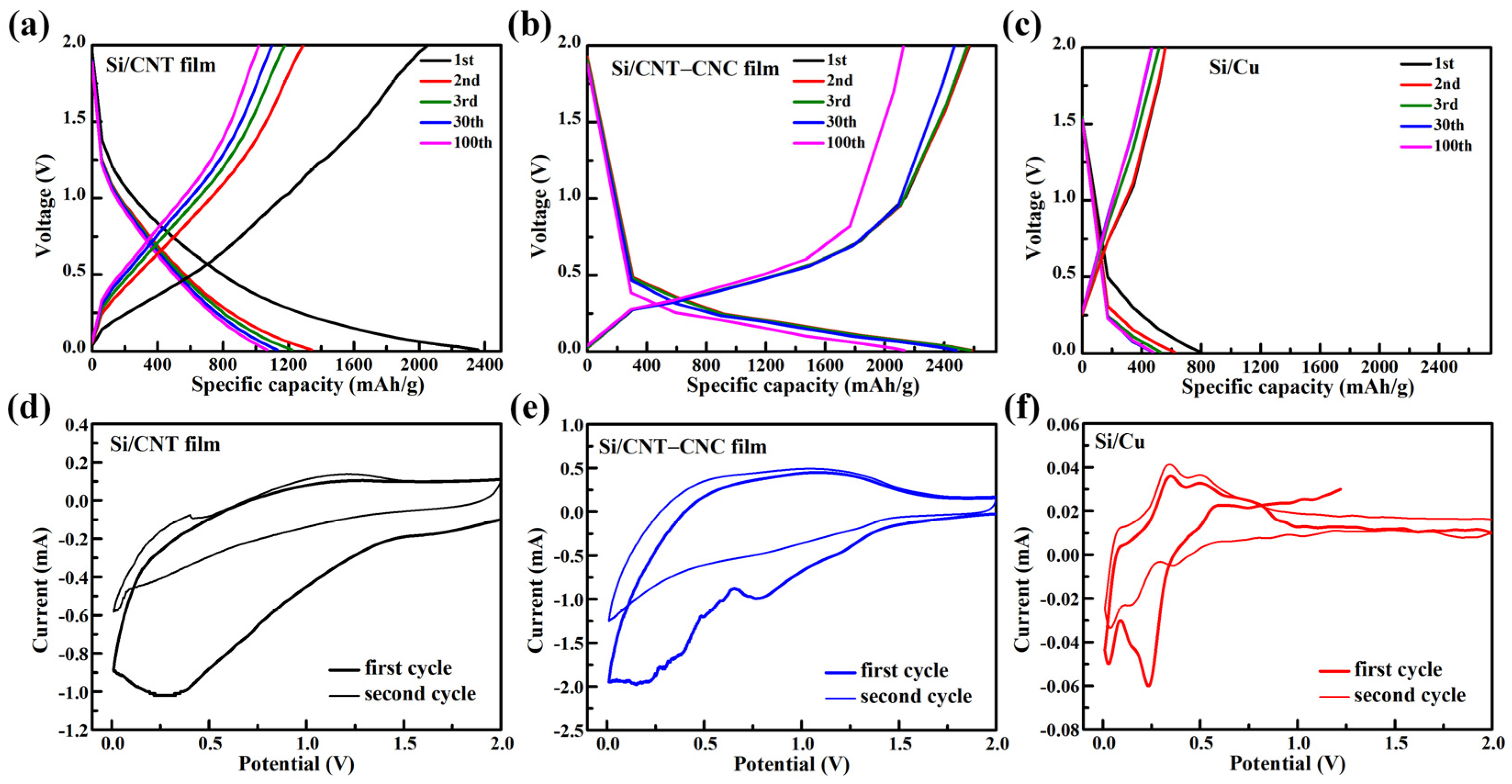
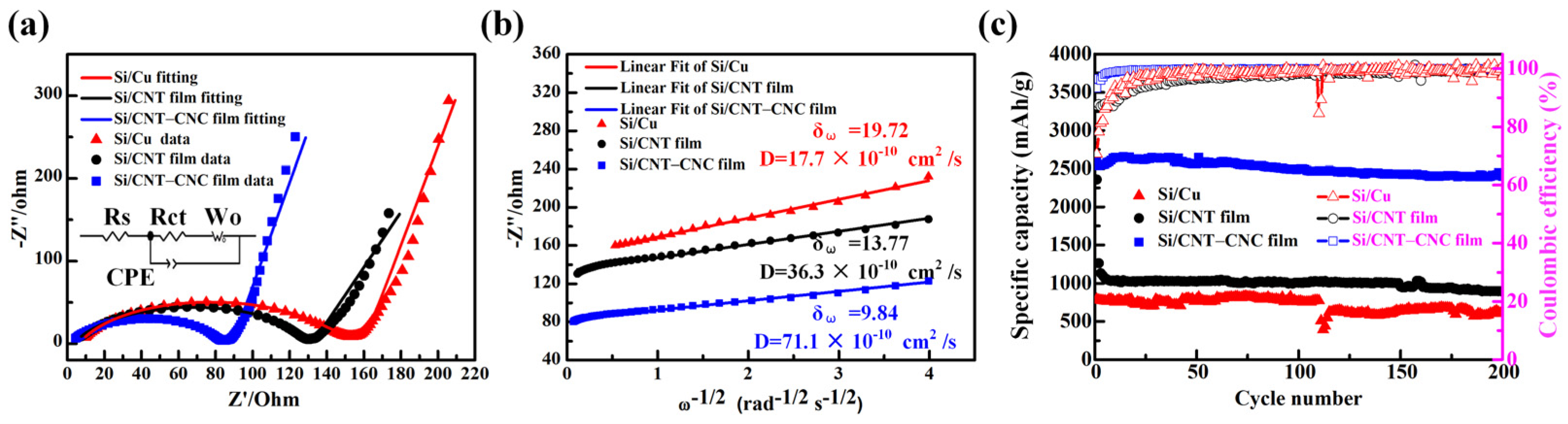
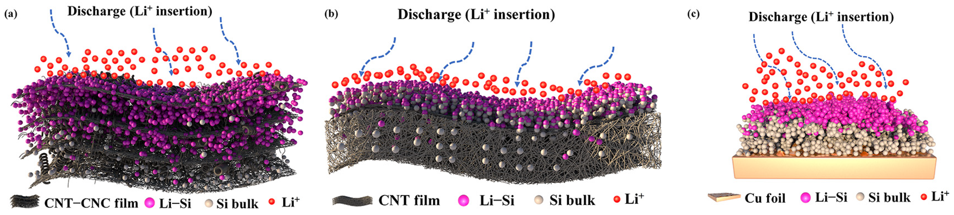
3.2. Electrochemical Performance of Cells

To examine the electrochemical performance of sputtered electrodes, Figure 3a−c depict the charge/discharge profiles of the 1st, 2nd, 3rd, 30th, and 100th cycles. As seen from Figure 3a, the charge/discharge capacities of the Si/CNT film electrode correspond to 2050/2359 and 1290/1340 mAh/g in the 1st and 2nd cycles, respectively. Due to the contribution of the Si deposition layer, the charge and discharge capacity of the electrode is greatly increased. Similarly, the charge and discharge capacity and coulomb efficiency of the Si/CNT–CNC film are increased, which delivers charge/discharge capacities of 2126/2131 mAh/g in the 100th cycle and a coulomb efficiency of 99.7% (Figure 3b). Compared with the Si/CNT film and the Si/CNT–CNC film electrode, the charge and discharge capacity of the Si/Cu electrode is the lowest, which delivers charge/discharge capacities of 558/792 mAh/g in the 100th cycle and a coulomb efficiency of 70.4% (Figure 3c). The initial columbic efficiency (ICE) for the Si/CNT film electrode is approximately 87%, which is much higher than that of the CNT film (17%, Figure S4). This irreversible capacity in the first cycle is primarily the result of the formation of a solid electrolyte interface (SEI) film on the surface of the active material. The improvement of the ICE is mainly due to the decrease in the surface area of the Si/CNT film electrode after it is sputtered with the Si deposition layer, which consumes less Li+ and less electrolytes. In addition, it can be concluded from Figure S4 that the electrochemical performance of the Si/CNT film and the Si/CNT–CNC film electrode is greatly improved after sputtering Si compared with the original CNT film and the CNT–CNC film.
As shown in Figure 3a–c, the Si/CNT film, the Si/CNT–CNC film and the Si/Cu electrode all have obvious sharp turning points in the discharge process, which may be because there are multiple reaction stages. First of all, at the beginning of discharge process the discharge curve is in a straight line and there is a significant voltage drop, which may be due to the adsorption of the charge. In the first discharge process, the voltage ranges of the Si/CNT film, the Si/CNT–CNC film and the Si/Cu electrode corresponding to the adsorption stage are about 2~1.3 V, 2~0.5 V and 1.5~0.5 V, respectively. It is evident that the adsorption stage of the Si/CNT–CNC film is the longest and the contribution of specific capacity is the largest. This is because the CNT–CNC film itself has a large surface area and a large number of pores, so it can absorb more charges at the beginning. Second, when the process of the adsorption process ends, the diffusion stage is dominant. The voltage ranges of the Si/CNT film, the Si/CNT–CNC film and the Si/Cu electrode corresponding to the diffusion stage are about 1.3~0.25 V, 0.5~0.25 V and 0.5~0.25 V, respectively. The diffusion process includes diffusion of lithium ions and formation of the SEI, which also corresponds to the first slope change. Finally, when the stable SEI is formed, the lithiation reaction begins, which is consistent with the Li+ embedded in the silicon at the voltage of 0.25 V. It is worth mentioning that lithium ions are embedded in the Si first, and then embedded they are in carbon, which is because the voltage of the lithium ion embedded in carbon is less than 0.2 V. As you can see from Figure 3a–c, in the Si/CNT–CNC film electrodes, the lithium ion takes the longest time to be embedded in the Si and contributes the most specific capacity, which indicates the high utilization of the Si.
The stage response of the charge/discharge curves of the Si/CNT film, the Si/CNT–CNC film, and the Si/Cu electrodes is consistent with the variation trend of the CV curves in Figure 3d–f. In Figure 3d, the voltage range of 2~1.3 V corresponds to the charge adsorption stage in the first cycle CV curve of the Si/CNT film electrode. When the voltage drops from 1.3 to 0.5 V, there is no obvious peak and the current starts to drop rapidly. This indicates that the decomposition process of the electrolyte and the formation of the SEI at this stage is relatively slow, which may be due to the good distribution of silicon in the CNT film. Finally, there is a distinct peak in the voltage range of 0.5~0.0 V, which corresponds to the embedding of the lithium ions into the Si. Similarly, as seen from Figure 3e, the current changes slowly during the voltage range of 2~0.5 V in the first cycle CV curve of the Si/CNT–CNC film electrode, which is due to the influence of the massive charge accumulation in the adsorption stage. At the same time, there is a small peak in this stage, which is due to the formation of the SEI. The peak disappeared completely in the second cycle, indicating that the formed SEI was stable. In Figure 3f, 1.5~0.5 V corresponds to the adsorption stage of the charge and the formation of the SEI. The apparent peak in 0.5~0 V corresponds to the lithium-ion embedded Si. Possibly due to the expansion and the rupture of the Si, the SEI formation of the first cycle is unstable; so in the second cycle, there is a peak corresponding the formation of the SEI in 1.5~0.5 V. There are no oxidation and reduction peaks in the CV curve of the Si/CNT film and the Si/CNT–CNC film electrodes. The possible reason is that the CNT film and the CNT–CNC film provide a large space for the Si uniform distribution, which provides more active sites for lithium ions; so the process of adsorption, diffusion and embedding of lithium ions occurs slowly, and the reaction is not violent.
During the charging process, the deembedding of lithium ions is divided into two stages. First, the voltage range of 0.1–0.4 V represents the separation of the lithium ions from carbon, so the Si/CNT film and the Si/CNT–CNC film electrodes have a wide peak in this interval, and the Si/Cu electrode does not appear to exhibit a similar phenomenon because there is no carbon component. This is consistent with the trend of the CV curve when the CNT film and the CNT–CNC film are separately used as anodes for LIBs. Then, in the voltage range of 0.5–1 V, all electrodes have a more obvious peak, which corresponds to the removal of the lithium ions from the Si. The difference is that the peaks of the Si/CNT film and the Si/CNT–CNC film are softer, and the peaks of the Si/Cu are sharper, because large quantities of lithium ions are simultaneously unembedded from the Si in the Si/Cu electrode. In addition, in the CV curve of the second cycle, the position of the peak does not change, but the strength increases, which indicates that the degree of activation of the material is further improved.
To further illustrate the enhanced electrochemical performance, the EIS test results were recorded. As shown in Figure 4a, the charge transfer resistance of the Si/CNT–CNC film electrode is the lowest, only ~85 Ω/cm2, which is due to having the thinnest Si deposition layer and the addition of carbon materials; the charge transfer resistance of the Si/CNT film and the Si/Cu electrode is 130 and 160 Ω/cm2, respectively. Then, we used Zview 3.1 software to establish an equivalent circuit model, fit the EIS curve in the low frequency region, and calculate the Li+ diffusion coefficient. The slope of the fitted curve corresponds to the Warburg coefficient δ ω , which is then calculated according to following equation:
D = R 2 T 2 2 A 2 n 4 F 4 C 2 δ ω   2
where R is the universal gas constant, T is the absolute temperature, A is the surface area of the electrode, n is the number of transferred electrons per molecule, F is Faraday constant and C is the concentration of Li+ [46].
The Li+ diffusion coefficients of the Si/CNT film, the Si/CNT–CNC film and the Si/Cu electrodes are 36.3 × 10⁻¹⁰, 71.1 × 10⁻¹⁰, and 17.7 × 10⁻¹⁰ cm2/s, respectively. It is worth emphasizing that the Li+ diffusion coefficient of the Si/CNT–CNC film is the highest, which indicates that the large holes on the surface of the CNT–CNC film provide channels for the transmission and diffusion of lithium ions so that lithium ions can be embedded easily.
The cyclic stability of the Si/CNT film, the Si/CNT–CNC film and the Si/Cu electrodes is compared throughout the 200 cycles at a current density of 50 mA/g, which is shown in Figure 4c. The ICE of the Si/CNT–CNC film is 93%, and the first discharge/charge capacities deliver 2586/2405 mAh/g. The Si/CNT film and the Si/Cu electrodes show 2359/2050 and 792/558 mAh/g, and the ICE values are 87 and 70%, respectively. With the cycle number increasing, the discharge capacity of the electrode decreases, and the Si/Cu electrode has a large fluctuation.
To deeper understand the excellent performance of the Si/CNT–CNC film anodes for LIBs, we propose three possible mechanisms to explain the reasoning. As illustrated in Figure 5, the pores on the surface and the inside of the CNT–CNC film significantly improve the way Si moves within the interior. The CNT–CNC film with 3D structure provides a large amount of storage space for Si due to its loose and porous surface, and the Si can penetrate into the deep part of the CNT–CNC film, thus resulting in the superficial thinnest Si deposition layer and the enhancement of energy storage and diffusion of the Li+ [47,48]. In contrast, the CNT film tends to agglomerate, reducing the surface area available for the Si and delaying its movement within the interior. Because of the densely compacted CNT film, a large amount of Si is deposited on the surface, with only a small amount of Si entering the inside of the CNT film. In the Si/Cu electrode, the Si deposition layer is all on the surface of the Cu foil, resulting in the low utilization of the Si. Therefore, the design of the 3D CNT–CNC film with interconnected ion transport channels and maximized exposure of active sites is crucial for achieving high performance. Lithium ions are first lithiated and delithiated on the surface of the electrode, and then they gradually conduct along the direction perpendicular to the surface of the electrode. During the discharge process, the region shows a positive charge after the lithium ions are embedded in the Si, while the other region is negatively charged due to the presence of a large number of electrons. This charge distribution exists on the surface and inside the Si/CNT–CNC film electrode and forms an electric field, which provides coulomb force to promote the rapid transmission of lithium ions. In the process of charging, there is also an inverse electric field, which is also conducive to the extraction of lithium ions. In addition, compared with crystalline Si films, the suspended bonds and defects in amorphous Si/CNT–CNC films provide a large number of active sites for Li+, which improves the storage capacity and the transport of lithium ions [35]

4. Conclusions

In this paper, Si is deposited on different substrates by magnetron sputtering. This current research focuses on the evaluation and comparison of the distribution of Si on the CNT film, the CNT–CNC film and the Cu foil. The electrodes after sputtering treatment are respectively named the Si/CNT film electrode, the Si/CNT–CNC film electrode and the Si/Cu electrode. We have investigated the longitudinal distribution of Si on the substrate surface as well as the vertical surface using SEM and EDS.
The CNT–CNC film with large pore structure provides enough space for the Si deposition, which improves the utilization of the Si deposition layer when it is used as the anode in LIBs. The specific capacity and cycle performance of LIBs with the Si/CNT–CNC film as the anode are the best and the reversible capacity is about 2500 mAh/g after 200 cycles, indicating the high utilization of Si and the rapid diffusion of lithium ions. In addition, the CNT–CNC film provides an elastic skeleton for the Si deposition layer, which eases the volume expansion of the Si during the charge and discharge processes. The Si/CNT–CNC film electrode provides an effective approach to obtain better performance and cyclic stability for LIBs.
From the above test results, it can be inferred that the substrate with a loose porous surface can effectively improve the utilization rate of Si and promote the diffusion of Li+. This can be used in applications where Si thin films are used as the anode in LIBs, which can improve the electrochemical performance and cycle performance of LIBs.

Supplementary Materials

The following supporting information can be downloaded at: https://www.mdpi.com/article/10.3390/jcs8090350/s1, Figure S1: The surface and cross-section morphology of silicon sputtered on CNT film at different powers (50 W, 75 W, 150 W); Figure S2: Charge and discharge curves of silicon sputtered on CNT film at different powers (50 W, 75 W, 150 W) at a specific current of 50 mA/g in the voltage window of 0.01~2.00 V (vs. Li/Li+); Figure S3: Raman spectra of Si/CNT–CNC film, Si/CNT film, Si/Cu, CNT film and CNT–CNC film electrodes; Figure S4: Galvanostatic charge/discharge profiles and cyclic voltammograms of CNT film, CNT–CNC film, Si/CNT film and Si/CNT–CNC film electrodes.

Author Contributions

Conceptualization, H.C. and L.P.; methodology, H.C., L.P. and L.H.; validation, H.C., C.W., Z.F. and L.P.; formal analysis, H.C.; investigation, H.C and C.C.; resources, C.C, L.H. and L.P.; data curation, H.C., Z.F. and L.P.; writing—original draft preparation, H.C.; writing—review and editing, H.C.; visualization, H.C. and L.P.; supervision, C.C and L.P.; project administration, L.P.; funding acquisition, L.P. All authors have read and agreed to the published version of the manuscript.

Funding

This work was financially supported by the National Natural Science Foundation of China [funder Lujun Pan, grant numbers 52272288, 51972039].

Data Availability Statement

The data presented in this study are available on request.

Acknowledgments

The authors also acknowledge the assistance of the DUT Instrumental Analysis Center.

Conflicts of Interest

The authors declare no conflicts of interest.

References

  1. Kim, T.; Song, W.T.; Son, D.Y.; Ono, L.K.; Qi, Y.B. Lithium-ion batteries: Outlook on present, future, and hybridized technologies. J. Mater. Chem. A 2019, 7, 2942–2964. [Google Scholar] [CrossRef]
  2. Wu, F.X.; Maier, J.; Yu, Y. Guidelines and trends for next-generation rechargeable lithium and lithium-ion batteries. Chem. Soc. Rev. 2020, 49, 1569–1614. [Google Scholar] [CrossRef] [PubMed]
  3. Ding, X.B.; Zhou, Q.F.; Li, X.D.; Xiong, X.H. Fast-charging anodes for lithium ion batteries: Progress and challenges. Chem. Commun. 2024, 60, 2472–2488. [Google Scholar] [CrossRef]
  4. Li, S.Q.; Wang, K.; Zhang, G.F.; Li, S.N.; Xu, Y.A.; Zhang, X.D.; Zhang, X.; Zheng, S.H.; Sun, X.Z.; Ma, Y.W. Fast Charging Anode Materials for Lithium-Ion Batteries: Current Status and Perspectives. Adv. Funct. Mater. 2022, 32, 2200796. [Google Scholar] [CrossRef]
  5. Zhang, S.C.; Du, Z.J.; Lin, R.X.; Jiang, T.; Liu, G.R.; Wu, X.M.; Weng, D.S. Nickel Nanocone-Array Supported Silicon Anode for High-Performance Lithium-Ion Batteries. Adv. Mater. 2010, 22, 5378–5382. [Google Scholar] [CrossRef] [PubMed]
  6. Sun, L.; Liu, Y.X.; Shao, R.; Wu, J.; Jiang, R.Y.; Jin, Z. Recent progress and future perspective on practical silicon anode-based lithium ion batteries. Energy Storage Mater. 2022, 46, 482–502. [Google Scholar] [CrossRef]
  7. Philippot, M.L.; Costa, D.; Cardellini, G.; De Sutter, L.; Smekens, J.; Van Mierlo, J.; Messagie, M. Life cycle assessment of a lithium-ion battery with a silicon anode for electric vehicles. J. Energy Storage 2023, 60, 106635. [Google Scholar] [CrossRef]
  8. Zhao, H.S.; Li, J.B.; Zhao, Q.; Huang, X.B.; Jia, S.Y.; Ma, J.M.; Ren, Y.R. Si-Based Anodes: Advances and Challenges in Li-Ion Batteries for Enhanced Stability. Electrochem. Energy Rev. 2024, 7, 36. [Google Scholar] [CrossRef]
  9. Ezzedine, M.; Zamfir, M.R.; Jardali, F.; Leveau, L.; Caristan, E.; Ersen, O.; Cojocaru, C.S.; Florea, I. Insight into the Formation and Stability of Solid Electrolyte Interphase for Nanostructured Silicon-Based Anode Electrodes Used in Li-Ion Batteries. Acs Appl. Mater. Inter. 2021, 13, 24734–24746. [Google Scholar] [CrossRef]
  10. Qi, Y.; Wang, G.; Li, S.; Liu, T.F.; Qiu, J.X.; Li, H.M. Recent progress of structural designs of silicon for performance -enhanced lithium -ion batteries. Chem. Eng. J. 2020, 397, 125380. [Google Scholar] [CrossRef]
  11. Park, M.H.; Kim, M.G.; Joo, J.; Kim, K.; Kim, J.; Ahn, S.; Cui, Y.; Cho, J. Silicon Nanotube Battery Anodes. Nano Lett. 2009, 9, 3844–3847. [Google Scholar] [CrossRef]
  12. Ling, M.; Xu, Y.N.; Zhao, H.; Gu, X.X.; Qiu, J.X.; Li, S.; Wu, M.Y.; Song, X.Y.; Yan, C.; Liu, G.; et al. Dual-functional gum arabic binder for silicon anodes in lithium ion batteries. Nano Energy 2015, 12, 178–185. [Google Scholar] [CrossRef]
  13. Azam, M.A.; Safie, N.E.; Ahmad, A.S.; Yuza, N.A.; Zulkifli, N.S.A. Recent advances of silicon, carbon composites and tin oxide as new anode materials for lithium-ion battery: A comprehensive review. J. Energy Storage 2021, 33, 102096. [Google Scholar] [CrossRef]
  14. Wang, J.; Zhao, R.R.; Yang, X.; Zhang, R.Y.; Guo, J.L.; Hao, J. Ionic liquids self-assembly preparation of binder-free composites anode with well-dispersed Si nanoparticles on CNTs networks for lithium-ion batteries. Appl. Surf. Sci. 2023, 618, 156655. [Google Scholar] [CrossRef]
  15. Chen, X.X.; Chen, Z.H.; Ni, Y.; Wang, L.; Sun, Y.M. Double-shell interphase design enabling suppressed side reactions for stable Si battery anode. Appl. Phys. Lett. 2022, 121, 123905. [Google Scholar] [CrossRef]
  16. Zhao, Z.Y.; Chen, F.Q.; Han, J.W.; Kong, D.B.; Pan, S.Y.; Xiao, J.; Wu, S.C.; Yang, Q.H. Revival of Microparticular Silicon for Superior Lithium Storage. Adv. Energy Mater. 2023, 13, 2300367. [Google Scholar] [CrossRef]
  17. Elomari, G.; Hdidou, L.; Larhlimi, H.; Aqil, M.; Makha, M.; Alami, J.; Dahbi, M. Sputtered Silicon-Coated Graphite Electrodes as High Cycling Stability and Improved Kinetics Anodes for Lithium Ion Batteries. Acs Appl. Mater. Inter. 2024, 16, 2193–2203. [Google Scholar] [CrossRef]
  18. Jiménez, A.R.; Klöpsch, R.; Wagner, R.; Rodehorst, U.C.; Kolek, M.; Nölle, R.; Winter, M.; Placke, T. A Step toward High-Energy Silicon-Based Thin Film Lithium Ion Batteries. Acs Nano 2017, 11, 4731–4744. [Google Scholar] [CrossRef]
  19. Tocoglu, U.; Cetinkaya, T.; Cevher, O.; Guler, M.O.; Akbulut, H. Nanostructured Silicon Thin Film Electrodes for Li-Ion Batteries. Acta Phys. Pol. A 2013, 123, 380–382. [Google Scholar] [CrossRef]
  20. Demirkan, M.T.; Trahey, L.; Karabacak, T. Cycling performance of density modulated multilayer silicon thin film anodes in Li-ion batteries. J. Power Sources 2015, 273, 52–61. [Google Scholar] [CrossRef]
  21. Xie, J.; Tong, L.; Su, L.W.; Xu, Y.W.; Wang, L.B.; Wang, Y.H. Core-shell yolk-shell Si@C@Void@C nanohybrids as advanced lithium ion battery anodes with good electronic conductivity and corrosion resistance. J. Power Sources 2017, 342, 529–536. [Google Scholar] [CrossRef]
  22. Chockla, A.M.; Harris, J.T.; Akhavan, V.A.; Bogart, T.D.; Holmberg, V.C.; Steinhagen, C.; Mullins, C.B.; Stevenson, K.J.; Korgel, B.A. Silicon Nanowire Fabric as a Lithium Ion Battery Electrode Material. J. Am. Chem. Soc. 2011, 133, 20914–20921. [Google Scholar] [CrossRef]
  23. Wang, L.; Gao, B.; Peng, C.J.; Peng, X.; Fu, J.J.; Chu, P.K.; Huo, K.F. Bamboo leaf derived ultrafine Si nanoparticles and Si/C nanocomposites for high-performance Li-ion battery anodes. Nanoscale 2015, 7, 13840–13847. [Google Scholar] [CrossRef] [PubMed]
  24. Wen, Z.H.; Lu, G.H.; Mao, S.; Kim, H.; Cui, S.M.; Yu, K.H.; Huang, X.K.; Hurley, P.T.; Mao, O.; Chen, J.H. Silicon nanotube anode for lithium-ion batteries. Electrochem. Commun. 2013, 29, 67–70. [Google Scholar] [CrossRef]
  25. Polat, B.D.; Keles, O. Improving Si Anode Performance by Forming Copper Capped Copper-Silicon Thin Film Anodes for Rechargeable Lithium Ion Batteries. Electrochim. Acta 2015, 170, 63–71. [Google Scholar] [CrossRef]
  26. Xie, J.; Imanishi, N.; Zhang, T.; Hirano, A.; Takeda, Y.; Yamamoto, O. Li-ion diffusion in amorphous Si films prepared by RF magnetron sputtering: A comparison of using liquid and polymer electrolytes. Mater. Chem. Phys. 2010, 120, 421–425. [Google Scholar] [CrossRef]
  27. Chen, X.; Bi, Q.S.; Sajjad, M.; Wang, X.; Ren, Y.; Zhou, X.W.; Xu, W.; Liu, Z. One-Dimensional Porous Silicon Nanowires with Large Surface Area for Fast Charge-Discharge Lithium-Ion Batteries. Nanomaterials 2018, 8, 285. [Google Scholar] [CrossRef]
  28. Schmuelling, G.; Winter, M.; Placke, T. Investigating the Mg-Si Binary System via Combinatorial Sputter Deposition As High Energy Density Anodes for Lithium-Ion Batteries. Acs Appl. Mater. Inter. 2015, 7, 20124–20133. [Google Scholar] [CrossRef]
  29. Tong, L.; Wang, P.; Chen, A.R.; Qiu, F.; Fang, W.Z.; Yang, J.; Wang, C.; Yang, Y. Improved electrochemical performance of binder-free multi-layered silicon/carbon thin film electrode for lithium-ion batteries. Carbon 2019, 153, 592–601. [Google Scholar] [CrossRef]
  30. Chai, L.; Wang, X.Y.; Su, B.; Li, X.G.; Xue, W.D. Insight into the decay mechanism of non-ultra-thin silicon film anode for lithium-ion batteries. Electrochim. Acta 2023, 448, 142112. [Google Scholar] [CrossRef]
  31. Chai, L.; Wang, X.Y.; Bi, C.J.; Su, B.; Zhang, C.; Li, X.G.; Xue, W.D. Lifetime Optimization of Amorphous Silicon Thin-Film Anodes for Lithium-Ion Batteries. Acs Appl. Energy Mater. 2023, 6, 8388–8396. [Google Scholar] [CrossRef]
  32. Tong, Y.F.; Xu, Z.; Liu, C.; Zhang, G.A.; Wang, J.; Wu, Z.G. Magnetic sputtered amorphous Si/C multilayer thin films as anode materials for lithium ion batteries. J. Power Sources 2014, 247, 78–83. [Google Scholar] [CrossRef]
  33. Ma, Y.T.; Li, L.; Qian, J.; Qu, W.J.; Luo, R.; Wu, F.; Chen, R.J. Materials and structure engineering by magnetron sputtering for advanced lithium batteries. Energy Storage Mater. 2021, 39, 203–224. [Google Scholar] [CrossRef]
  34. Tocoglu, U.; Cevher, O.; Guler, M.O.; Akbulut, H. Coaxial silicon/multi-walled carbon nanotube nanocomposite anodes for long cycle life lithium-ion batteries. Appl. Surf. Sci. 2014, 305, 402–411. [Google Scholar] [CrossRef]
  35. Tong, L.; Wang, P.; Fang, W.Z.; Guo, X.J.; Bao, W.Z.; Yang, Y.; Shen, S.L.; Qiu, F. Interface Engineering of Silicon/Carbon Thin-Film Anodes for High-Rate Lithium-Ion Batteries. Acs Appl. Mater. Inter. 2020, 12, 29242–29252. [Google Scholar] [CrossRef]
  36. Farmakis, F.; Elmasides, C.; Fanz, P.; Hagen, M.; Georgoulas, N. High energy density amorphous silicon anodes for lithium ion batteries deposited by DC sputtering. J. Power Sources 2015, 293, 301–305. [Google Scholar] [CrossRef]
  37. Schulze, M.C.; Urias, F.; Dutta, N.S.; Huey, Z.; Coyle, J.; Teeter, G.; Doeren, R.; de Villers, B.T.J.; Han, S.D.; Neale, N.R.; et al. Control of nanoparticle dispersion, SEI composition, and electrode morphology enables long cycle life in high silicon content nanoparticle-based composite anodes for lithium-ion batteries. J. Mater. Chem. A 2023, 11, 5257–5266. [Google Scholar] [CrossRef]
  38. Yang, Y.Z.; Yang, Z.; Li, Z.L.; Wang, J.; He, X.M.; Zhao, H.L. Rational Electrolyte Design for Interfacial Chemistry Modulation to Enable Long-Term Cycling Si Anode. Adv. Energy Mater. 2023, 13, 2302068. [Google Scholar] [CrossRef]
  39. Landi, B.J.; Ganter, M.J.; Cress, C.D.; DiLeo, R.A.; Raffaelle, R.P. Carbon nanotubes for lithium ion batteries. Energ. Environ. Sci. 2009, 2, 638–654. [Google Scholar] [CrossRef]
  40. Coppey, N.; Noé, L.; Dupin, J.C.; Puech, P.; Vergnes, H.; Monthioux, M.; Caussat, B. Silicon Nanoparticle/Carbon Nanotube Composites for LI-ION Battery Anodes. Carbon 2012, 17–22. [Google Scholar]
  41. Shi, Q.T.; Zhou, J.H.; Ullah, S.; Yang, X.Q.; Tokarska, K.; Trzebicka, B.; Ta, H.Q.; Rümmeli, M.H. A review of recent developments in Si/C composite materials for Li-ion batteries. Energy Storage Mater. 2021, 34, 735–754. [Google Scholar] [CrossRef]
  42. Chen, H.; Zhao, Y.P.; Zhao, H.T.; Huang, H.; Wen, N.X.; Wang, C.; Fan, Z.; Hao, L.; Pan, L.J. Hybrid films constructed by carbon nanotubes and carbon nanocoils as current collectors for lithium-ion batteries. J. Electroanal. Chem. 2023, 935, 117288. [Google Scholar] [CrossRef]
  43. Chen, H.; Wang, C.; Fan, Z.; Hao, L.; Pan, L.J. Facile fabrication of binder-free carbon nanotube-carbon nanocoil hybrid films for anodes of lithium-ion batteries. J. Solid. State Electr. 2024, 28, 3325–3335. [Google Scholar] [CrossRef]
  44. Zhao, Y.P.; Wang, J.Z.; Huang, H.; Cong, T.Z.; Yang, S.T.; Chen, H.; Qin, J.Q.; Usman, M.; Fan, Z.; Pan, L.J. Growth of Carbon Nanocoils by Porous α-Fe2O3/SnO2 Catalyst and Its Buckypaper for High Efficient Adsorption. Nano-Micro Lett. 2020, 12, 23. [Google Scholar] [CrossRef]
  45. Zhao, Y.P.; Zhang, H.; Yang, X.; Huang, H.; Zhao, G.L.; Cong, T.Z.; Zuo, X.Q.; Fan, Z.; Yang, S.T.; Pan, L.J. In situ construction of hierarchical core-shell Fe3O4@C nanoparticles-helical carbon nanocoil hybrid composites for highly efficient electromagnetic wave absorption. Carbon 2021, 171, 395–408. [Google Scholar] [CrossRef]
  46. Zhao, H.T.; Chen, H.; Wang, C.; Fan, Z.; Hao, L.; Pan, L.J. Three-dimensional porous framework constructed by hybrid of carbon nanotubes and carbon nanocoils for stable lithium metal anode. J. Mater. Res. 2022, 37, 2073–2081. [Google Scholar] [CrossRef]
  47. Leong, I.W.; Tsutsui, M.; Yokota, K.; Murayama, S.; Taniguchi, M. Regulating Nonlinear Ion Transport through a Solid-State Pore by Partial Surface Coatings. Acs Appl. Mater. Inter. 2023, 15, 6123–6132. [Google Scholar] [CrossRef]
  48. Divya, M.L.; Lee, Y.S.; Aravindan, V. Solvent Co-intercalation: An Emerging Mechanism in Li-, Na-, and K-Ion Capacitors. Acs Energy Lett. 2021, 6, 4228–4244. [Google Scholar] [CrossRef]
Figure 1. The surface morphology of different CCs before and after sputtering and the interfacial morphology and contact between different CCs and Si after sputtering at 75 W. (ad) Si/CNT film-75 W electrode. (eh) Si/CNT–CNC film-75 W electrode. (il) Si/Cu-75 W electrode.
Jcs 08 00350 g001
Figure 2. The EDS of surface and cross-section of Si/CNT–CNC film and Si/CNT film. (a,b) Surface and cross-section distribution of elements in Si/CNT–CNC film. (c,d) Surface and cross-section distribution of elements in CNT film.
Jcs 08 00350 g002
Figure 3. The electrochemical performance of Si/CNT film, Si/CNT–CNC film and Si/Cu electrodes as anodes. (ac) Galvanostatic charge/discharge profiles. (df) CV curves at the first two cycles.
Jcs 08 00350 g003
Figure 4. (a) EIS data fitting and equivalent circuit model building. (b) Calculation results of the Li+ diffusion coefficient. (c) Cyclic stability of Si/CNT film, Si/CNT–CNC film and Si/Cu electrodes.
Jcs 08 00350 g004
Figure 5. Schematic illustration of the Li+ embedded three different electrodes. (a) Si/CNT–CNC film electrode. (b) Si/CNT film electrode. (c) Si/Cu electrode.
Jcs 08 00350 g005
Disclaimer/Publisher’s Note: The statements, opinions and data contained in all publications are solely those of the individual author(s) and contributor(s) and not of MDPI and/or the editor(s). MDPI and/or the editor(s) disclaim responsibility for any injury to people or property resulting from any ideas, methods, instructions or products referred to in the content.

