Proceeding Paper

An Investigation of the Synthesis of a Hybrid Homogeneous Structure of ZnO/Si Nanowires with Stable Energy Properties †

1
Institute of Physics and Technology, Satbayev University, Almaty 050013, Kazakhstan
2
Microelectronics Department, Saint-Petersburg State Electrotechnical University, 5 Professora Popova Street, 197376 Saint-Petersburg, Russia
3
Alferov Federal State Budgetary Institution of Higher Education and Science Saint Petersburg National Research Academic University of the Russian Academy of Sciences, 194021 Saint-Petersburg, Russia
*
Author to whom correspondence should be addressed.
Presented at the 3rd International Electronic Conference on Processes—Green and Sustainable Process Engineering and Process Systems Engineering (ECP 2024), 29–31 May 2024; Available online: https://sciforum.net/event/ECP2024.
Eng. Proc. 2024, 67(1), 28; https://doi.org/10.3390/engproc2024067028
Published: 3 September 2024
(This article belongs to the Proceedings of The 3rd International Electronic Conference on Processes)

Abstract

:
The stability of structures to various influences determines the effectiveness of the sensors that are based on them. A modified method of metal-stimulated electrochemical etching and hydrothermal etching made it possible to synthesize the combined structure of silicon nanowires and ZnO crystallites. The hexagonal structure of zinc oxide crystallites was determined by the X-ray diffraction method. Several causes of radiative recombination have been identified in the photoluminescence spectra, and their nature is associated with the defective structure of zinc oxide. Electron paramagnetic resonance (EPR) spectroscopy studies have revealed energy-stable, uniformly distributed and low-dimensional nanostructures.

1. Introduction

Nowadays, reducing the size of materials leads to the discovery of new effects that improve the parameters of devices. The surface structure, in the form of nanorods and nanowires, has an increased specific surface area and, consequently, a high concentration of centers of interaction with the environment. These properties enhance the sensitivity of the sensor based on these structures.
The determination of charge transfer features in nanowires makes it possible to understand the main processes in low-dimensional systems [1]. However, differences in the coefficients of thermal expansion and lattice constants between surface nanostructures and the substrate lead to significant stresses. This causes the growth of randomly oriented nanowires and the deterioration of the entire structure.
In this regard, nanostructures grown on a porous surface attract special attention. The work in [2] shows a decrease in deformation and an increase in the number of points of growth for one-dimensional structures grown on a rough surface of porous silicon (PS). An important parameter in this case is the morphology of the pore walls. This affects the distribution of charges and their movement in the channel structure.
The deposition of zinc oxide onto the branched mesoporous structure of silicon can lead to the blocking of local pore constrictions by ZnO particles. This causes the formation of structures in a certain direction. The use of porous silicon with smooth walls, uniform in direction, avoids channel overlap. This leads to a more homogeneous filling of the pores [3].
The lasers with a broadening radiation spectrum are promising applications of ZnO/PS structures. The combination of green radiation from the ZnO defects band, blue UV radiation from the ZnO excitons and red radiation from the PS layers can lead to the desired effect [4]. These structures can also be the basis of photosensitive sensors.
Another relevant application of ZnO/PS is in memristive devices. Memristive switching has been observed in many metal oxides [5,6] and is explained by the migration of vacancies in oxide layers and at grain boundaries [7,8]. Despite this, the charge transfer mechanisms are still a subject of discussion and various models are assumed [6,7,8]. On the other hand, PS-ZnO composites can be used to adjust the grain size of ZnO. This leads to the possibility of manufacturing a storage device by adjusting the surface structure and vacancy concentration. This makes it possible to obtain a configurable device response, especially in the case of hierarchical porous surfaces [9].
The purpose of these studies is to create an energy-stable hybrid of ZnO/PS structures with an increased specific surface area as the basis for the sensor material.
The spatial distribution of nanostructures plays an important role in the sensor mechanisms. The novelty of these studies is associated with the synthesis of a substance with a uniform distribution of low-dimensional structures over the surface of the sample.
During the long-term operation of the sensor, its characteristics decrease. Therefore, it is very important to determine the stability to exposure of the sensor material. The next point of novelty of the research is to identify the energy stability of structures determined by the EPR method.

2. Materials and Methods

2.1. Synthesis of the Studied Samples

The synthesis of porous silicon nanowires was carried by the method of two-stage modified metal-stimulated electrochemical etching (MAESE) [10,11]. The synthesis was carried out in galvanostatic mode. First, the electrochemical etching of a monocrystalline silicon plate (p-Si (100), specific resistance 12 Ohm*sm) is carried out to form a composite of porous silicon and silver nanoparticles on its surface. The process took place in an aqueous alcohol solution of hydrogen fluoride (HF) and silver nitrate (AgNO3) with a concentration of 0.01 M. The duration of the process was 4.5 min, and the anodizing current density was 15 mA/cm2.
This method allows the deposition of silver nanoparticles on the surface of a porous matrix, without penetration of silver into the depth of the porous layer. The use of silver is explained by its high catalytic activity. The electrolyte at the first stage contains the following components: water, alcohol, hydrofluoric acid and AgNO3. Water is an oxidizer (oxidation of Si to SiO2) and hydrofluoric acid is an etching reagent (etches SiO2). Alcohol helps to improve the wettability of the silicon wafer with the electrolyte. AgNO3 serves as a source of silver.
At the second stage, the electrochemical etching of the obtained samples is performed in an aqueous alcohol solution of hydrofluoric acid (for 20 min at 120 mA/cm2), with the formation of wire structures. The silver deposited on the surface of the plate promotes intensive local oxidation and the subsequent spot etching of the oxidized area in hydrofluoric acid. Further, the samples were washed sequentially in isopropyl alcohol and distilled water.
The synthesis of ZnO is implemented in the following stages. At the first stage, the formation of the nucleus layer was carried out. For this purpose, 56 mg of zinc acetate ((CH3COO)2Zn) was dissolved in 50 mL of isopropyl alcohol. Then, the solution is deposited by centrifugation at 3000 rpm for 30 s on the porous surface. After that, the samples are dried at 150 °C for 5 min. To achieve a high concentration of ZnO nanoparticles in the pores of porous silicon nanowires (which are the growth centers of zinc oxide nanowires), the procedure was repeated 5 times. After that, the sample was annealed at 350 °C for 30 min.
At the second stage, the layer with wires was formed by a low-temperature hydrothermal method. For this purpose, zinc acetate Zn(O2CCH3)2 = 175.6 mg, H2O = 80 mL, Hexamethylenetetramine = 112.1 mg, and STAV (Cetrimonium bromide) = 27.6 mg were used. The resulting solution was placed with a thermostat and kept at 86 °C for 1 h. After synthesis, the samples were annealed at 500 °C for 5 min. The final annealing was carried out in an air atmosphere at a temperature of 200 °C for 1 h.

2.2. Characterization Methods
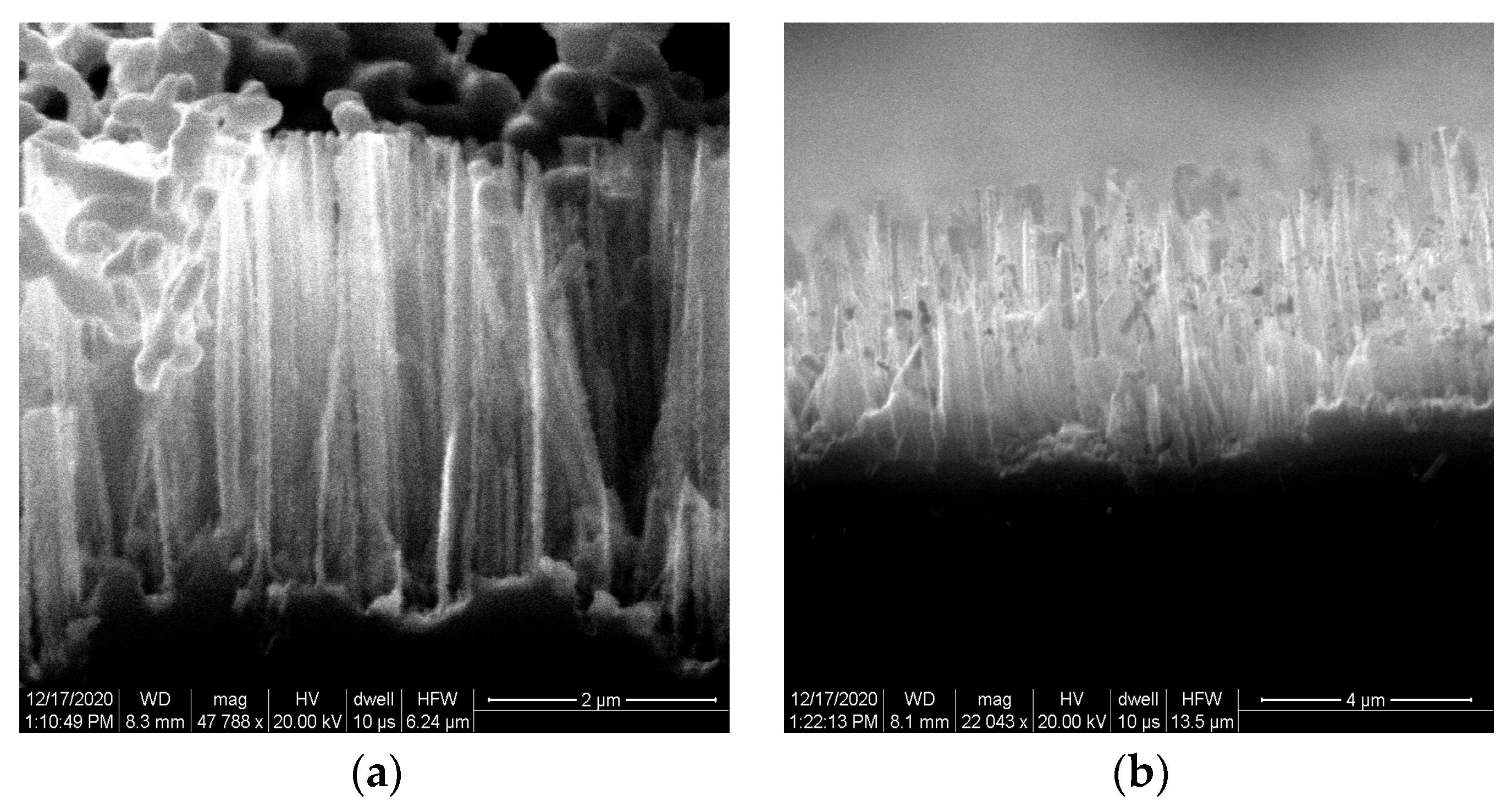
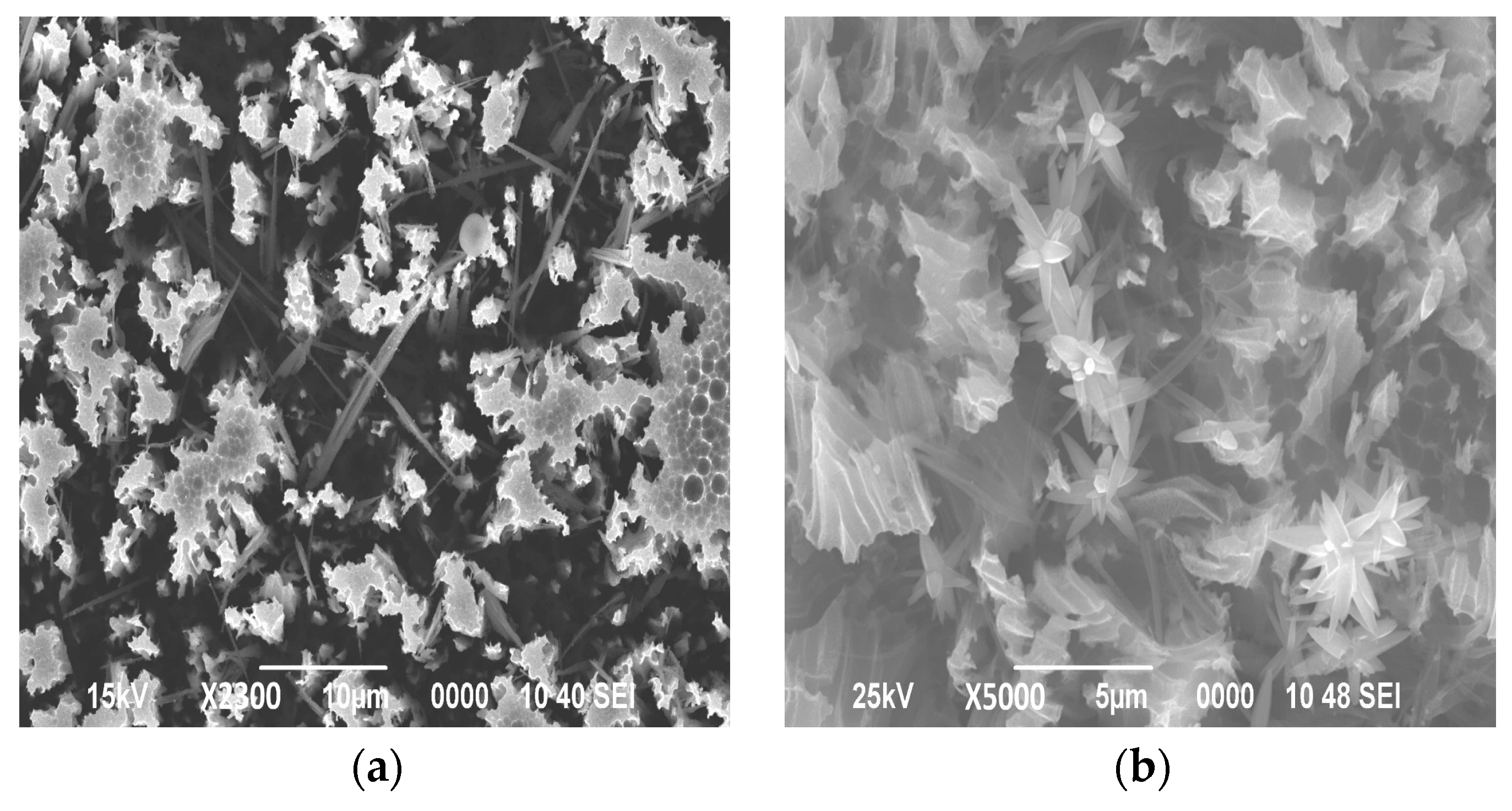
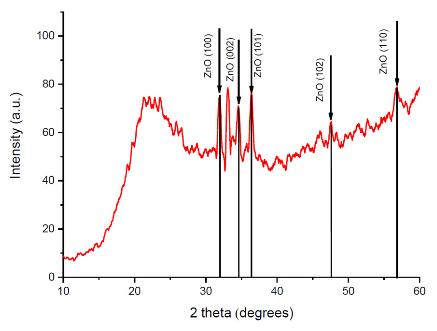
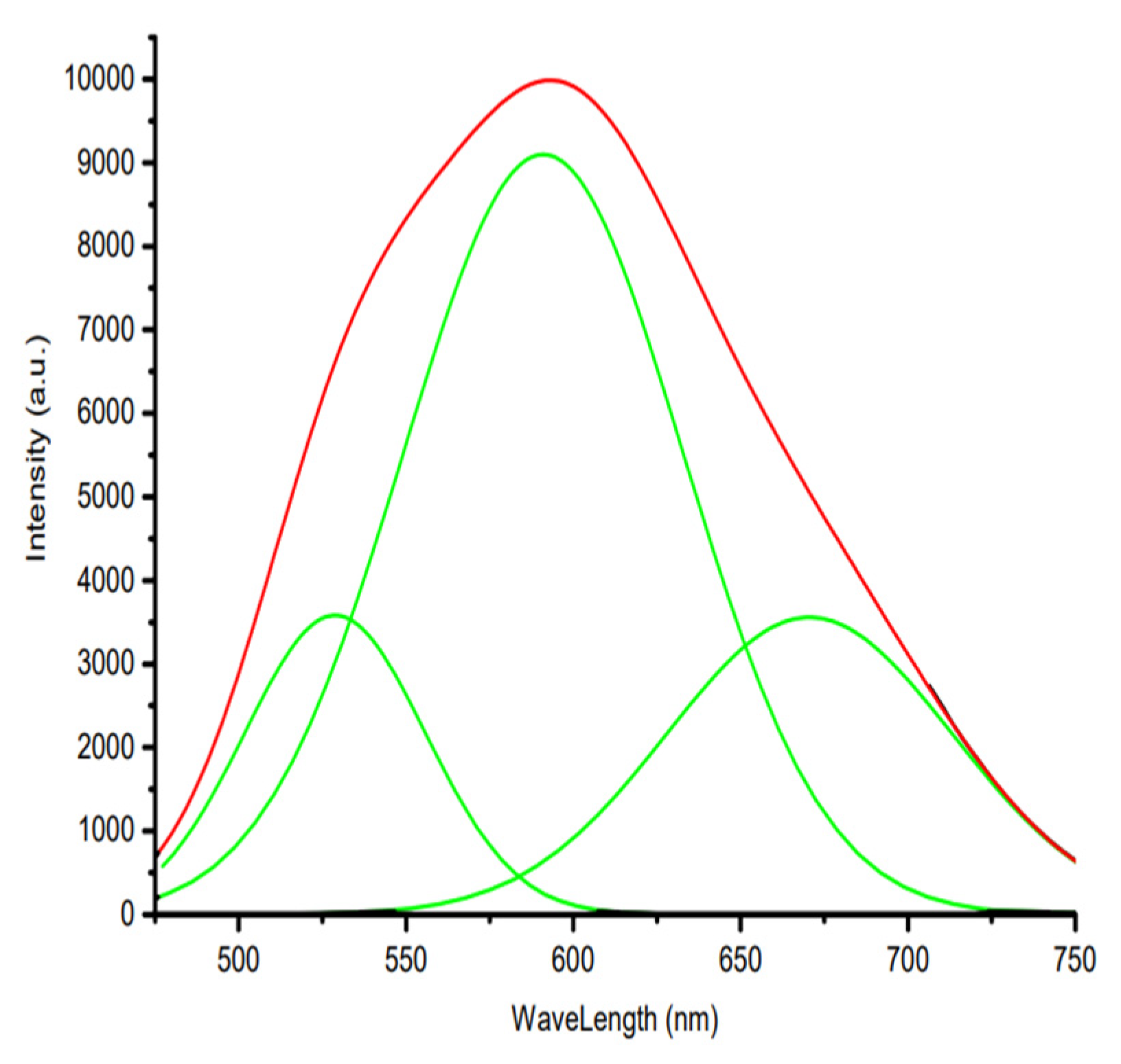
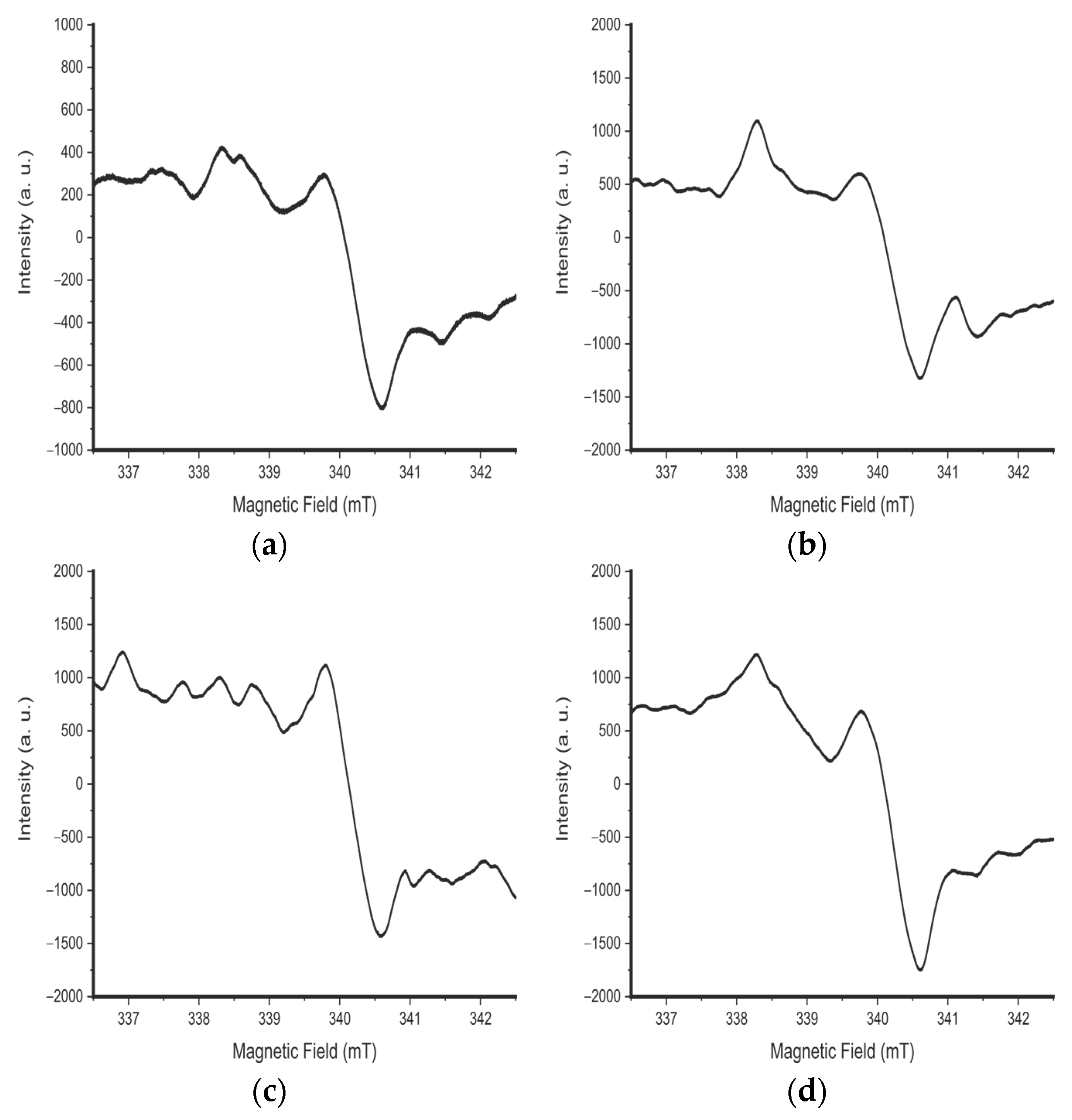
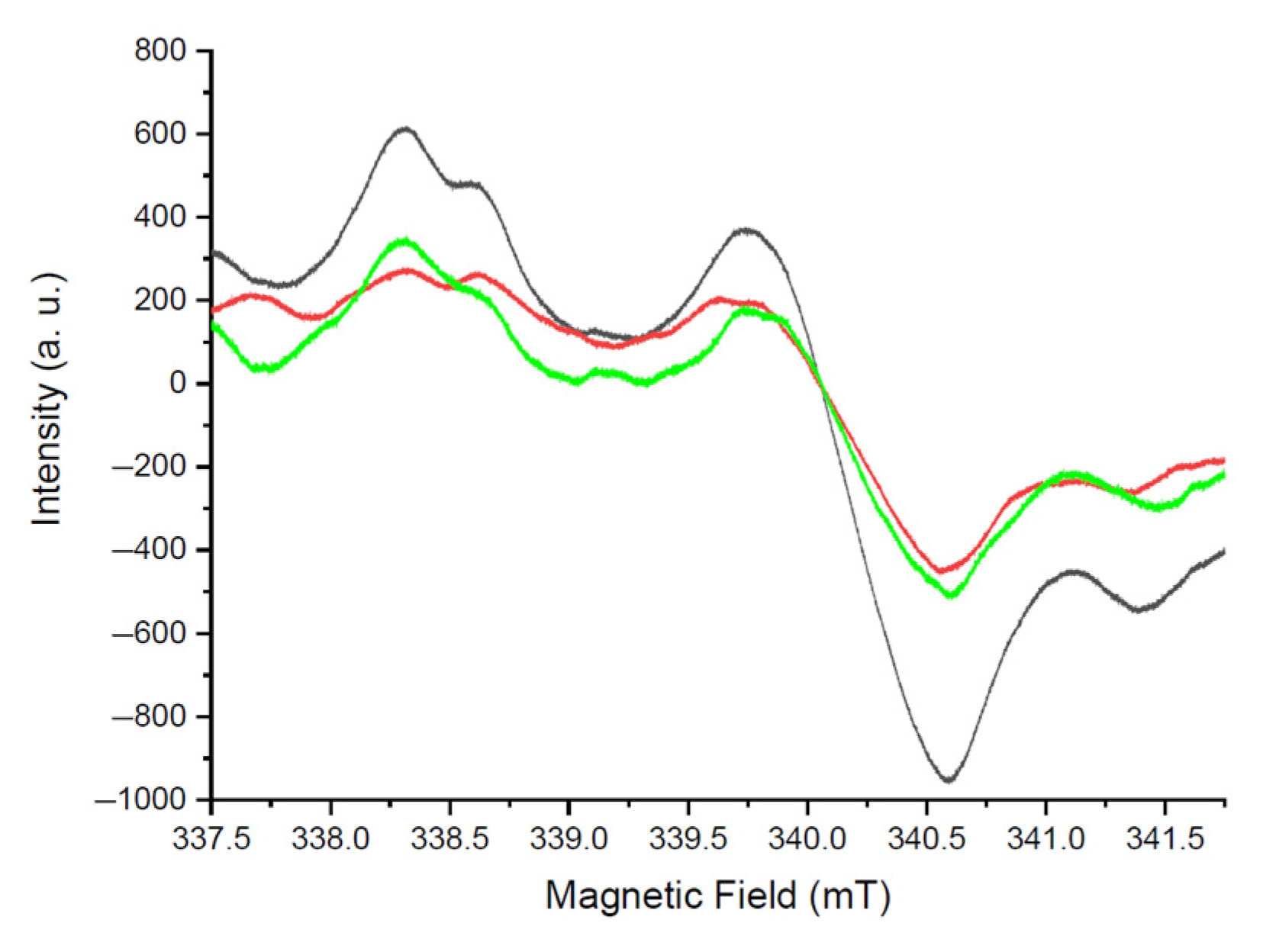
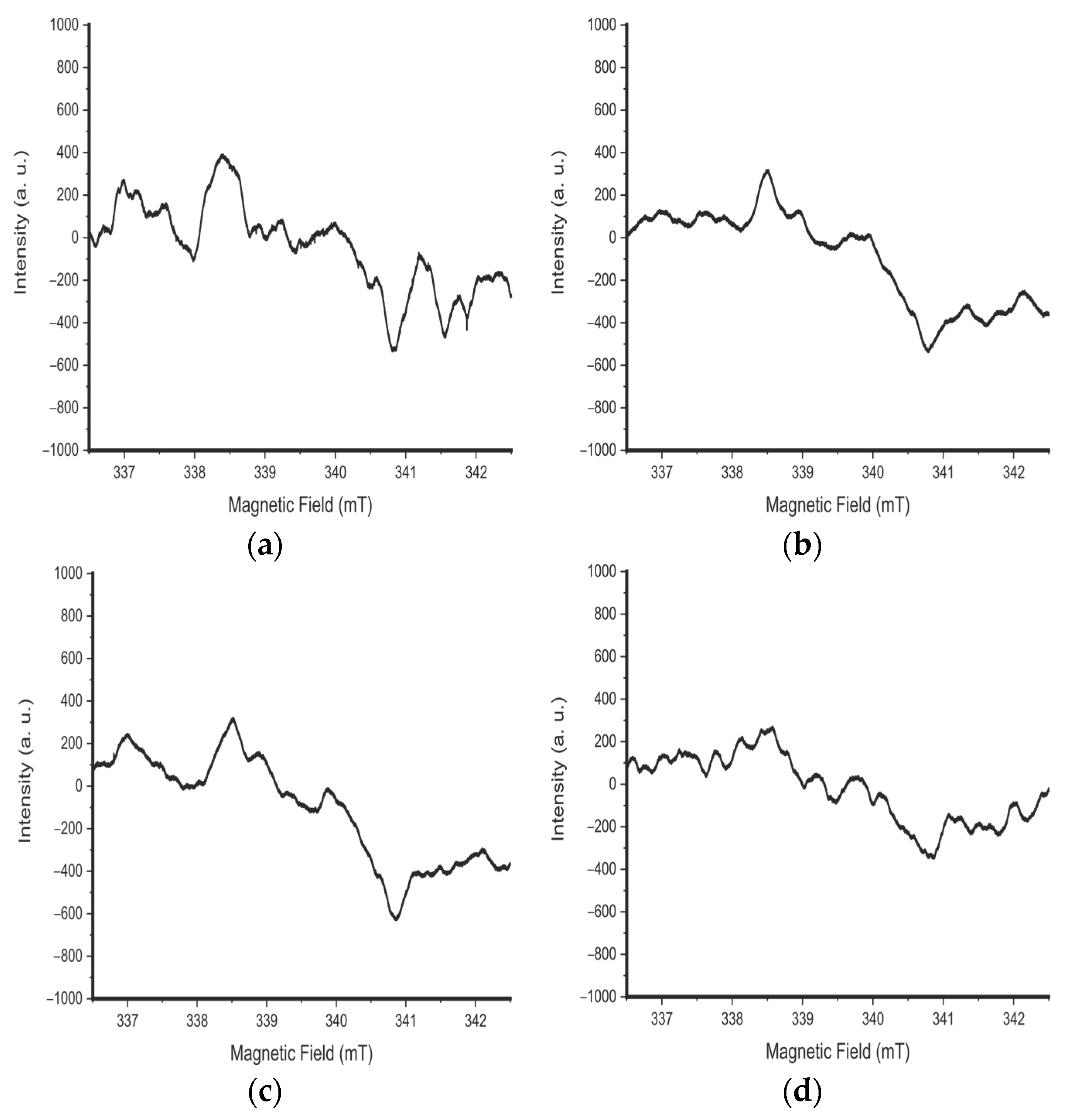
X-ray diffraction was used to study the structure of the surface layer of the samples. A highly collimated (0.05 × 1.5) mm2 monochromatic (CuKα) X-ray beam was focused at a 5° angle to the sample’s surface. The intensity of the X-ray reflections along the debaegram was measured every 2 = 0.05° using a microdensitometer. The Jones technique was used to determine the average size of the crystallites based on the half-width of the X-ray lines.
A scanning electron microscope (SEM), JSM-6490LA (“JEOL”, Akishima, Japan), was used. The take-off angle for the JSM-6490LA is 35°, and the analytical working distance is 10 mm. The microscope has a resolution of 3.0 nm. The elemental analysis of the samples was carried out on an analytical scanning electron microscope, JSM 6490 LA by JEOL, equipped with the JED 2300 EDS spectrometer.
Photoluminescence (PL) was recorded in the range of zinc oxide defects from 400 to 800 nm using a Cary Eclipse spectrophotometer (Agilent, Santa Clara, CA, USA). The spectral width of the slit in this device varies from 0.5 to 2.4 nm. A tungsten–halogen lamp served as the radiation source for visible measurements.
The “JEOL” EPR spectrometer (JES-FA200, Akishima, Japan) can measure in the 9.4 GHz (X-Band) and 35 GHz (Q-Band) ranges. The microwave frequency stability is ~10−6. The sensitivity = 7 × 10⁹/10−4 Tl. The resolution is 2.35 μT. The output power ranges from 200 mW to 0.1 μW, with a quality factor (Q-factor) of 18,000.

3. Results

The morphology of the surface has been studied at all stages of its transformation. These include the formation of silicon wires, the synthesis of ZnO/PS structures, and the samples after annealing at 200 °C in an air atmosphere.
Studies of the morphology of the surface of the samples after the synthesis of silicon nanowires showed a homogeneous structure (Figure 1). The directions of one-dimensional structures are predominantly vertical. The height of the nanowires ranged from 2.58 to 4.22 microns and the average thickness was 292.6 nm.
The images after ZnO deposition (Figure 2) show areas with nanowires, as well as structures similar to flowers, turning into larger structures. It is assumed that the flower-like zinc oxide crystallites grow at the ends of the silicon nanowires. The elemental analysis of the structures showed the highest concentration for zinc. The presence of silicon and oxygen was also determined (Table 1).
The surface of the sample after ZnO deposition and annealing (t = 200 °C, 1 h, air atmosphere) consists of clusters of individual nanowires, structures similar to flowers, and structures of more complex configurations formed by fused wires and flowers (Figure 3). Such a variety determines the transformation of one-dimensional structures.
The structure of crystallites plays an important role in the processes of substance activity. X-ray diffraction studies have shown mainly the presence of a hexagonal structure of zinc oxide crystallites on the sample surface (Figure 4). The average crystallite size is shown in Table 2 [12].
An important indicator of the quality of the synthesis of structures is the change in photoluminescent characteristics. After annealing of the sample, a photoluminescence spectrum was obtained (Figure 5). The spectrum is decomposed into several components, which indicates the presence of several causes of radiative recombination.
The nature of photoluminescence is related to the defective structure of zinc oxide. The basic particles for zinc oxide nanostructures are oxygen vacancies, F-centers and their complexes. Radiation occurs when a charge is captured on a vacancy [13]. A change in the energy level of the vacancies inside the band gap significantly affects the mechanism and intensity of photoluminescence.
EPR studies effectively complement information about defects, in particular in nonradiative recombination. The measurements took place with a sequential increase in microwave power. Studies have shown the presence of a narrow signal for the sample after ZnO deposition (Figure 6), which does not change in shape over a wide range of microwave power (from 1 mW to 19 mW). On the one hand, this indicates the predominance of low-dimensional structures with a certain direction in the samples. On the other hand, this is due to the energy stability of these structures.
Subtraction of the spectra before annealing (Figure 7) shows that with an increase in power in the range up to 8 mW, the signal does not saturate and neither does it become significantly wider. This is related to the continuous transition of charges from the ground energy state to the excited one. This is due to the presence of free energy exchange between homogeneous spins and the crystal lattice for structures with a high degree of organization.
Under the influence of heat treatment, paramagnetic structures are transformed when the properties of a substance changes. The EPR studies after annealing (200 °C, air atmosphere, 1 h) showed a significant broadening of the signal, which was narrow for the sample before annealing (Figure 8). The signal intensity decreases, and its saturation occurs at 9 mW.
The signal widening is associated with the unification of nanowires and the enlargement of floral-like structures. The signal intensity reduces due to an increase in the number of interconnected structures. A decrease in the saturation power threshold for the sample after annealing is associated with a decrease in the stability of the structures under the selected temperature mode. The properties of the sensor material vary depending on its heating. Thus, for these structures, heat treatment at a temperature of 200 °C reduces the efficiency of the device.

4. Conclusions

A uniform structure of silicon nanowires was formed using the modified MAESE method. As a result of zinc oxide deposition, flower-like crystallites were synthesized at the ends of silicon nanowires. Annealing of the samples at 200 °C in air atmosphere led to the enlargement of the crystallites. Studies of photoluminescence in the zinc oxide defective spectral region have shown the presence of several causes of radiative recombination. EPR studies of samples after ZnO formation showed the presence of a narrow-width signal. This spectrum did not change in shape with a sequential increase in microwave power. Thus, the formation of energetically stable, low-dimensional structures uniformly distributed in the sample volume is proved. Annealing at 200 °C in air atmosphere led to a broadening of the EPR spectrum and a decrease in the signal intensity. Moreover, the EPR signal saturation threshold was reduced after annealing. This indicates a decrease in the stability of the structures under this heat treatment mode.

Author Contributions

Conceptualization, R.Z.; methodology, T.S.; software, A.K. and Y.S.; validation, Y.S.; formal analysis, K.N. and V.M.; investigation, A.G. and D.M.; resources, A.K.; data curation, M.B.; writing—original draft preparation, T.S.; writing—review and editing, A.G. and D.M.; visualization, A.K.; supervision, M.B. and R.Z.; project administration, R.Z.; funding acquisition, V.M. and E.D. All authors have read and agreed to the published version of the manuscript.

Funding

This research was funded by the Science Committee of the Ministry of Science and Higher Education of the Republic of Kazakhstan (Grant No. BR21881954 «Development of technologies for the synthesis of nanostructured materials for efficient photocatalytic electrodes, photo- and gas-sensors»).

Institutional Review Board Statement

Not applicable.

Informed Consent Statement

Not applicable.

Data Availability Statement

The original contributions presented in the study are included in the article, further inquiries can be directed to the corresponding author.

Conflicts of Interest

The authors declare no conflict of interest.

References

  1. Wang, X.; Song, J.; Wang, Z.L. Nanowire and nanobelt arrays of zinc oxide from synthesis to properties and to novel devices. J. Mater. Chem. 2007, 17, 711–720. [Google Scholar] [CrossRef]
  2. Abdulgafour, H.I.; Hassan, Z.; Yam, F.K.; Jawad, M.J. Growth of ZnO nanowires without catalyst on porous silicon. AIP Conf. Proc. 2011, 1341, 18–20. [Google Scholar]
  3. Sherstnev, A.I.; Chubenko, E.B.; Redko, S.V.; Petrovich, V.A.; Pilipenko, V.A.; Bondarenko, V.P. Formation of nanocomposite materials based on porous silicon and zinc oxide by electrochemical method. Rep. Belarusian State Univ. Inform. Radioelectron. 2016, 95, 82–88. [Google Scholar]
  4. Hsu, H.C.; Cheng, C.S.; Chang, C.C.; Yang, S.; Chang, C.S.; Hsieh, W.F. Orientation-enhanced growth and optical properties of ZnO nanowires grown on porous silicon substrates. Nanotechnology 2005, 16, 297. [Google Scholar] [CrossRef] [PubMed]
  5. Yang, J.J.; Pickett, M.D.; Li, X.; Ohlberg, D.A.; Stewart, D.R.; Williams, R.S. Memristive switching mechanism for metal/oxide/metal nanodevices. Nat. Nanotechnol. 2008, 3, 429–433. [Google Scholar] [CrossRef] [PubMed]
  6. Sawa, A. Resistive switching in transition metal oxides. Mater. Today 2008, 11, 28–36. [Google Scholar] [CrossRef]
  7. Zoolfakar, A.S.; Kadir, R.A.; Rani, R.A.; Balendhran, S.; Liu, X.; Kats, E.; Bhargava, S.K.; Bhaskaran, M.; Sriram, S.; Zhuiykov, S.; et al. Engineering electrodeposited ZnO films and their memristive switching performance. Phys. Chem. Chem. Phys. 2013, 15, 10376–10384. [Google Scholar] [CrossRef] [PubMed]
  8. Liu, L.; Chen, B.; Gao, B.; Zhang, F.; Chen, Y.; Liu, X.; Kang, J. Engineering oxide resistive switching materials for memristive device application. Appl. Phys. A 2011, 102, 991–996. [Google Scholar] [CrossRef]
  9. Martínez, L.; Ocampo, O.; Kumar, Y.; Agarwal, V. ZnO-porous silicon nanocomposite for possible memristive device fabrication. Nanoscale Res. Lett. 2014, 9, 437. [Google Scholar] [CrossRef] [PubMed]
  10. Gagarina, A.Y.; Bogoslovskaya, L.S.; Spivak, Y.M.; Novikova, K.N.; Kuznetsov, A.; Moshnikov, V.A. Synthesis of arrays nanostructured porous silicon wires in electron conductivity type silicon with crystallographic orientation (111). Tech. Phys. 2023, 68, 254. [Google Scholar] [CrossRef]
  11. Nalimova, S.S.; Gagarina, A.I.; Spivak, I.M.; Bobkov, A.A.; Kondratev, V.M.; Bolshakov, A.D.; Moshnikov, V.A. Chemoresistive Gas Sensor and Method for Its Manufacture. Russian Patent RU 2806670 C1, 2 November 2023. [Google Scholar]
  12. Mukhamedshina, D.; Mit’, K.; Chuchvaga, N.; Tokmoldin, N. Fabrication and study of sol-gel ZnO films for use in Si-based 716 heterojunction photovoltaic devices. Mod. Electron. Mater. 2017, 3, 158–161. [Google Scholar] [CrossRef]
  13. Murzalinov, D.; Seredavina, T.; Kemelbekova, A.; Spivak, Y.; Moshnikov, V.; Mukhamedshina, D.; Fedosimova, A. Investigation of Surface Nanoclusters and Paramagnetic Centers of ZnO/Por-Si Structures as the Basis of Sensory Properties. Processes 2023, 11, 3332. [Google Scholar] [CrossRef]
Figure 1. SEM images of the structure of silicon nanowires in the samples before the deposition of zinc oxide with a magnification of (a) 2 microns and (b) 4 microns.
Engproc 67 00028 g001
Figure 2. SEM image of the sample surface after ZnO deposition with a magnification of (a) 10 microns and (b) 5 microns.
Engproc 67 00028 g002
Figure 3. SEM image of the sample surface after ZnO deposition and annealing with a magnification of (a) 2.5 microns and (b) 1 micron.
Engproc 67 00028 g003
Figure 4. XRD spectra of samples after ZnO deposition and annealing.
Engproc 67 00028 g004
Figure 5. Photoluminescence spectrum (red line) decomposed into gaussians (green line) for the sample after ZnO deposition and annealing.
Engproc 67 00028 g005
Figure 6. EPR spectra of samples after ZnO deposition at microwave powers of (a) 4 mW, (b) 12 mW, (c) 15 mW and (d) 18.7 mW.
Engproc 67 00028 g006
Figure 7. Subtraction of EPR spectra at microwave powers of 6 mW and 1.5 mW: 6 mW—black line, 1.5 mW—red line, result of subtraction—green line.
Engproc 67 00028 g007
Figure 8. EPR spectra of samples after ZnO deposition and annealing at microwave powers of (a) 4 mW, (b) 6.2 mW, (c) 7.8 mW and (d) 11 mW.
Engproc 67 00028 g008
Table 1. The results of the elemental analysis of the flower-like structures.
Fitting Coefficient: 0.3890
Element(kEV)Mass%At%
O0.5252.487.77
Si1.73917.1030.53
Zn8.63080.4261.70
Total 100.00100.00
Table 2. Average size of ZnO crystallites in films.
Average Size of Crystallites in the Plane, nm
ZnO (100)ZnO (002)ZnO (101)ZnO (102)
38.8741.7826.7122.11
Disclaimer/Publisher’s Note: The statements, opinions and data contained in all publications are solely those of the individual author(s) and contributor(s) and not of MDPI and/or the editor(s). MDPI and/or the editor(s) disclaim responsibility for any injury to people or property resulting from any ideas, methods, instructions or products referred to in the content.

