Abstract
This study presents an automated methodology for evaluating micro-channels fabricated using a femtosecond laser on stainless steel substrates. We utilize 3D surface topography and metrological analyses to extract geometric features and detect fabrication defects. Standardized samples were analyzed using a light interferometer, and the resulting data were processed with Principal Component Analysis (PCA) and RANSAC algorithms to derive channel characteristics, such as depth, wall taper, and surface roughness. The proposed method identifies common defects, including bumps and V-defects, which can compromise the functionality of micro-channels. The effectiveness of the approach is validated by comparisons with commercial solutions. This automated procedure aims to enhance the reliability and precision of femtosecond laser micro-milling for industrial applications. The detected defects, combined with fabrication parameters, could be ingested in an AI-based process to optimize fabrication processes.
1. Introduction
The constant push for lighter and smaller components in almost all the industrial markets (e.g., medical, microelectronics, energy, and consumer electronics) is driving the development of innovative fabrication processes that can provide high-quality, precise miniaturized components at a cost.
Different technologies have been developed in the past years to provide sub-millimeter components with reasonable precision and repeatability [1]. CNC micro-milling uses high-precision positioning systems and a high-speed rotation tool to remove material and shape the component [2]. The main factors limiting the feature dimension with micro-milling are the tool’s dimensions and the cutting edge’s radius. The precision is also limited by the deformation of the tool given by the force acting on it when it is in contact with the material to be removed [3]. Moreover, due to the friction, the tool is subjected to wear and must be replaced sooner or later depending on the hardness of the processed materials. Micro Electro Discharge Machining (Micro-EDM), on the other hand, is a non-contact process that employs electric discharges between the electrode tool and the workpiece to erode material [4]. Even if it is a non-contact method, the discharge damages the electrode tool [5]. The workpiece needs to be surrounded by a dielectric liquid to avoid unwanted electrical sparks. Since an electric discharge deposits the energy, this technique only works with conductive materials limiting its applications.
Since its introduction in the industry, laser technology has experienced a huge evolution, contaminating every field thanks to its flexibility [6,7]. Lasers can perform heavy-duty tasks like welding, cutting, and drilling thick metal for manufacturing mechanical components, or extremely precise tasks such as shaping the cornea to eliminate sight problems [8,9,10,11,12]. Compared to micro-milling and EDM, lasers offer various advantages. Laser material processing does not require a tool, thus avoiding friction and wear, and can be used with any kind of material, including dielectric materials such as glass [13]. Among all the laser types available for industrial applications, recently ultra-short pulsed (USP) lasers, especially femtosecond pulsed lasers, have attracted increasing attention thanks to the reduced Heat Affected Zone (HAZ). In femtosecond lasers, the energy is deposited on the surfaces of the piece to be machined in pulses with a temporal width of hundreds of femtoseconds. The high intensity combined with the short pulse duration leads to the material removal from the surface before the electrons have the chance to interact with the crystal lattice, dissipating the energy and heating the nearby area. Through this process, often referred to as cold ablation, HAZ is reduced, allowing precise and controlled micromachining of components [14,15,16]. Femtosecond pulsed lasers have been used for producing micrometric features in a large variety of materials and for multiple applications [17,18,19,20,21,22]. Among the possible processes, femtosecond micro-milling consists of removal by laser ablation of the material layer by layer until the final shape is engraved into the material surface. This technique can be used to create groves with controlled shapes for friction control [23], to shape pillars for lower contact resistance in Solid Oxide Fuel Cells (SOFCs) [24], to create 3D electrodes for lithium-ion batteries [25], or to fabricate various electronic microdevices [26,27], to mention some.
However, despite the huge potential, femtosecond laser micromachining processes are very difficult to optimize [28]. This is demonstrated by the ongoing effort to search for new optimization strategies based on machine learning and artificial intelligence [28,29,30,31,32].
Imperfections in the geometries to be realized by laser micro-milling can be harmful to its successive application [33]. Therefore, process optimization becomes crucial to avoid defect formation in the workpiece. Common defects that can arise in the process are wrong depth, rough bottom, or presence of bump.
This work proposes an automated method, based on 3D surface topography and metrological analyses, to examine and detect relevant geometrical features in micro-channels fabricated by micro-milling with a femtosecond laser in stainless steel. Using in-house machine-standardized samples, we developed an automated procedure to acquire the topography data of several micro-channels with a light interferometer (Section 2.1 and Section 2.2). The collected data were then processed using Principal Component Analysis (PCA) at multiple scales and RANSAC algorithms for plane recognition and segmentation (Section 2.3) to derive micro-channels’ geometric characteristics, including depth and wall taper. The quality of the bottom plane was evaluated through the roughness value and the evaluation of the bump’s presence. The procedure wants to automatically detect milling defects like bumps and V-defects. Bumps are artifacts on the bottom of the ablated region appearing when a critical temperature is reached [34]. These irregularities hamper the quality of the channels decreasing their quality. On the other hand, V-defects are narrow trenches located at the intersection between the bottom and the walls parallel to the channel walls. They can reach several microns in depth.
To evaluate the proposed metrological procedure, comparisons with data provided by a commercial solution are performed.
2. Materials and Methods
2.1. Sample Preparation and Femtosecond Laser
The micro-channels were fabricated on a 15.0 mm × 15.0 mm AISI 316BA steel substrate. The laser source used for the sample preparation was a Pharos PH1 (Light Conversion, Vilnius, Lithuania) with a fundamental wavelength of 1030 nm. The laser beam was focused on the substrate surface through an F-Theta lens (focal length 100 mm) and moved across the surface with a galvanometer scanner excelliSCAN 14 (SCANLAB, Puchheim, Germany). The laser process parameters were changed over a wide range to cover a large parameter space. In particular:
- -
- the pulse energy was varied between 0.2 µJ and 37 µJ;
- -
- the laser spot diameter on the sample was modified by a motorized beam expander MEX18 (OPTOGAMA, Vilnius, Lithuania) between 13 µm and 60 µm;
- -
- the minimum value of the repetition rate used was 50 kHz whereas the maximum was 606 kHz.
- -
- the laser scanning velocity was set to obtain a pitch between 1.3 µm and 30 µm;
- -
- the line spacing parameter was set to the same range of values.
The laser beam scanning strategy over the small surface, in the x and y plane, is schematized in Figure 1. The scanning strategy is repeated multiple times to ablate several layers of material from the sample until the micro-channel is formed. The acceleration and deceleration areas were located outside the micro-channel and the laser was triggered to shoot only in the area of constant speed to avoid pulse accumulation. The micro-channels were all machined with the same multi-angle strategy, whereas the laser scanning direction to the channel walls is alternated at each repetition. Each steel substrate can host multiple micro-channel matrices, as shown in Figure 2a.
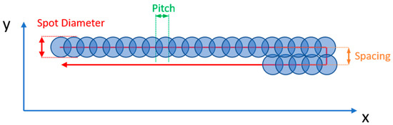
Figure 1.
Scheme of the laser beam scanning strategy in the x, y plane. The red arrow indicates the scanning direction, and the blue circles represent the laser pulse distribution on the sample surface. The darker blue areas show the laser pulse overlapping.
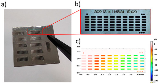
Figure 2.
(a) Picture of a steel substrate with multiple micro-channel matrices for the sample creation. (b) Optical microscope image of a single matrix containing 60 micro-channels (120 µm × 300 µm, various depths), round markers at the corners, and the identification code. (c) Sample topography was obtained by stitching multiple acquisitions performed with the white light interferometer. In the color scale, 0 corresponds to the surface of the substrate where the micro-channels were micro-machined.
2.2. Data Acquisition and Preparation
Each matrix contains 60 micro-channels (120 µm × 300 µm) arranged in 10 columns by 6 rows grid (Figure 2b). From the optical microscope picture, the single micro-channels, the marker, and the sample identification code can be clearly distinguished. The 3D acquisition of the matrix was performed by a compact interferometer (smart WLI, GBS mbH, Ilmenau, Germany) equipped with a 20× Nikon Mirau interferometric objective and a motorized x,y stage. The field of view was fixed to 909 µm × 567 µm given the combination of the objective and the camera sensor. To acquire the full matrix, the white light interferometer was used in stitching mode and each tile corresponds to the field of view. The spacing between the micro-channels was chosen to match the tiles’ dimensions, i.e., each tile contains complete micro-channels. This precaution avoids placing the intersection of tiles in the middle of a micro-channel that could introduce stitching errors in the region of interest. The resulting sample topography of a single matrix (60 micro-channels) is reported in Figure 2c. The interferometer was programmed to automatically acquire multiple matrices along the same substrate. To do so, the stages moved to the desired location at the top right corner of the first matrix and started the stitching procedure. When the matrix acquisition is complete, the files are saved, the full matrix is reconstructed, and the stage is automatically moved to the next matrix. To reduce the overall acquisition time, multiple substrates can be positioned on the motorized stage, and they can be acquired without human intervention.
To detect the fiducial markers located at the corners of each matrix, a binary threshold is applied to the collected 3D data (Figure 3). The markers (100 µm in diameter with a depth of 40 µm) were fabricated right after the micro-channel fabrication without moving the sample so that the location of the channel to the marker is known. Given their asymmetric distribution, once the center of the fiducial markers is identified, it is possible to locate each micro-channel and eliminate outlier points. The point clouds of the separated channels are saved separately and an identification code, composed of matrix ID, row, and column indices, can be used to keep track of the specific laser parameters used.
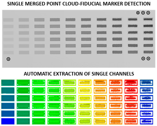
Figure 3.
Micro-channels separation from markers. The entire point cloud of a matrix with fiducial markers highlighted (top). The point cloud of the matrix with the single micro-channels automatically separated (bottom). Colors represent the different depths of the micro-milled regions.
2.3. Shape Analyses with Geometric Feature Extraction
The relevant geometric properties in a micro-channel are its depth and the roughness of the bottom plane. Using a laser beam with a Gaussian intensity profile leads to the formation of inclined walls. The wall taper depends on various laser parameters such as laser fluence, spot diameter, focal length, and scanning speed [35]. To properly evaluate the channel characteristics and correlate them to the laser parameters, 3D geometric features [36] are derived for each channel’s point cloud. These features have proved to successfully support 3D data interpretation and analyses for many applications [37,38]
For each point of the cloud, a local covariance matrix through principal component analysis is computed using specific radii [39,40,41]. Eigenvalues () are combined to calculate a set of local features (normally with a range [0, 1]), such as verticality, planarity, surface variation, and omnivariance (Table 1, [42]).

Table 1.
Local 3D features (ranges [0, 1]) used to analyze the channels.
The verticality feature distinguishes horizontal flat areas (low values) from surfaces with a more significant vertical (and noisy) component. The surface variation allows us to distinguish if a point belongs to a flat area (low values) or to an edge area (high values). The omnivariance is a geometric attribute commonly applied to describe the local 3D structure around a point: low values mean regular surfaces. The planarity is used to identify the bottom surfaces of the micro-machined channels. High values belong to horizontal surfaces, and low values depict vertical ones.
Using these features, points are segmented according to whether they belong to side walls or to the bottom of the channel. Then, using RANSAC and a least squares fitting process, planes are extracted, and point-to-plane distances are computed to evaluate the quality of the micro-milling work (Figure 4). For each of the four vertical walls, the normal vector n for the best-fitting plane is computed. The nz component of the fitted plane is used to calculate the angle between the micro-machined wall and the surface from which the channel is machined. A 90° angle corresponds to a perfectly vertical wall. The average of the four angles is calculated as θ.
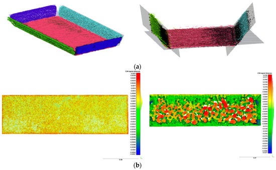
Figure 4.
Plane fitting concept to identify walls and bottom of two different micro-machined channels (a). Points to ideal plane distances to evaluate milling defects (b): smooth bottom with low roughness (left) and bumpy bottom (right).
The STATUS parameter (Table 2) considers if at least 70% of the points have a planarity higher than 0.9.
Table 2.
Geometric characteristics are derived for each channel.
The irregularity of a surface is evaluated by calculating its roughness (Ra, Table 2). The surface roughness can be considered as the feature of not being smooth and could be linked to the human perception of the surface texture. The roughness is quantified by the deviation, in the direction of the normal vector, of a real surface from its ideal form.
To detect the presence of bumps on the micro-channel’s bottom, the BUMPS_SCORE parameter is used: we consider the percentage of points in the bottom plane with a surface variation (computed with a radius of 50 μm) higher than 0.025. Scores close to 1 mean a few bumps on the bottom.
For the V-defects, 8 ROIs (Figure 5) are identified and points inside those areas are used to compute the V_DEPTH and V_CORNERS_DEPTH parameters (Table 2). The V_DEPTH parameter is computed in the regions along the intersection of the four walls (blue areas in Figure 5) as the difference between the average Z in that area and the average Z of the bottom plane. The V_DEPTH_CORNES parameter is computed in the same way but for areas at the corners of the micro-channel in order to consider defects arising from reflections at the intersection of two vertical walls.
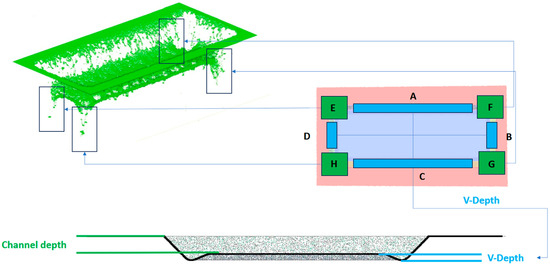
Figure 5.
The different ROIs where V-defects are sought are colorized in light blue (along the sides) and green (at the corners). The points contained in the blue regions are used to compute the V_DEPTH parameter. Points in the green regions are used for the estimation of V_CORNERS_DEPTH.
2.4. Workflow for Data Analyses
To collect, analyze, store, and visualize thousands of experimental data derived from thousands of micro-machined samples, a specific workflow was realized (Figure 6). When a micro-channel is machined, the operator can input the database of the laser and process parameters through a specific user interface. After each fabrication, the samples are analyzed with a white light interferometer that reconstructs the 3D surface of the specimen and saves the resulting point cloud data (Section 2.2). The saved data are then prepared to be analyzed by the classification process, which extracts the metrological information from the point cloud data (Section 2.3). The extracted values are saved and matched with the fabrication details thanks to a unique identification code used as a key in the database. Although the 3D reconstruction is performed with a white light interferometer, the developed methodology could be used with other instruments that provide as output a point cloud of the micro-machined samples.
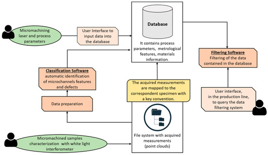
Figure 6.
The developed workflow–dataflow for analyzing the micro-machined channels.
The core of the workflow is the MySQL database (version 8.0.23), where all the data of the laser process and metrological information are stored. As shown in Figure 6, using a dedicated user interface (Figure 7), the operator inputs the laser process parameters used to create the samples into the database. The surfaces of the fabricated samples are then acquired and digitalized with the light interferometer and the resulting point cloud data are saved. The raw data are then prepared before being processed by the classification software, which extracts the metrological information about the micro-channel. The data preparation step is needed to transform the raw data from the interferometer into the proper format required by the classification software.
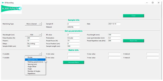
Figure 7.
The realized GUI to support users in storing the milling parameters.
The metrological information about the micro-channel features is then automatically saved into the database. When the operator inputs the micromachining parameters of the sample, each micro-channel is assigned a unique identification code (ID), which is subsequently used as a key to match the results from the classification software and the input parameter from the operator. Therefore, the laser process parameters and derived metrological information are associated with each micro-channel, identified by its ID. This information can finally be visualized through a user interface upon request.
3. Results and Discussion
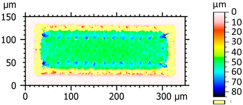
Following the reported methodology, Figure 8 shows the 3D surface reconstruction and analysis of four micro-channels with different characteristics. The c channel presents no defects and a smooth bottom layer. Channel d has a higher surface roughness on the bottom plane. Channels a and b instead present visible defects. The former shows a very rough bottom plane with the presence of melting defects (i.e., bumps). The latter, although has a nice and smooth bottom layer, shows V-defects along all sides, clearly visible in dark blue. Depending on the application and use of such channels, rough bottoms, bumps, or V-defects can be harmful and must be avoided.
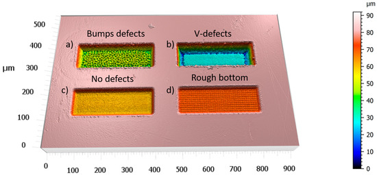
Figure 8.
Micro-channels (a,b,c,d) and their 3D surface reconstruction, featuring a very rough bottom with the presence of bumps defects (a), deeper depth and low roughness bottom with V-defects along all walls intersections (b), no defects and smooth bottom surface (c), and a shallow depth with an intermediate roughness between channels a and c (d). In the visual representation and color legend, the lower depth is at 0 μm (dark blue) whereas the higher points at at 90 μm (light pink).
On the same micro-channels, covariance features (Section 2.3) are extracted to analyze their shapes and find irregularities (Figure 9). The planarity parameter is useful to classify the overall quality of the channels: indeed, the higher the planarity the lower the defects and roughness of walls and bottom plane. For the micro-channels without bumps defects, the planarity values are generally higher than 0.9 at the bottom plane. Micro-channel b shows a prominent decrease in planarity at the intersection of the bottom plan and walls, due to the presence of V-defects and bumps. The omnivariance is generally less than 0.1 on smooth and planar surfaces while it clearly increases with the presence of bumps and V-defects along the bottom plane borders. Combining omnivariance and surface variation parameters, bump defects can be clearly distinguished with a considerable difference between walls and regular bottom planes. The verticality, for micro-channels without bumps defects, is useful to separate walls (high values) from the bottom plane (low values).
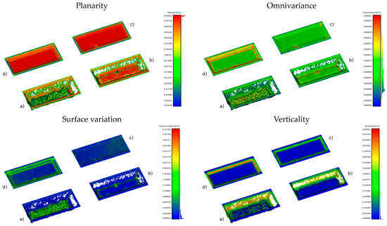
Figure 9.
Extracted covariance features on the micro-machined channels of Figure 8: planarity, omnivariance, surface variation, and verticality. The missing points on some micro-channel walls are a consequence of the interferometer’s light scattering. Some parts of the inclined and rough walls might reflect to the microscope objective a quantity of light below the instrument sensitivity.
Figure 10 shows some close-up views of three different bottom channels and values of computed characteristics. The absence of bumps is represented by high values of the BUMP_SCORE (BS) or low values of roughness. It is worth noticing that for flat and regular surfaces, the roughness values computed by the proposed methodology (Sas) and the commercial software MountainsMap of the GBS interferometer (Sai) are quite similar. On the other hand, when bumps are present, the two roughness values are more far apart. This is probably due to the fact that MountainsMap uses ISO 25178 (Available online: https://www.iso.org/standard/74591.html (accessed on 23 July 2024)) for the extraction of profile and surface parameters, including Sa. Moreover, the software applies a Gaussian S-filter (in the manual, they refer to ISO 16610-61 (Available online: https://www.iso.org/standard/60813.html (accessed on 23 July 2024))), which cuts off wavelengths smaller than 1 μm (which is slightly larger than 2× the pixel size). This operation is performed on a central portion of the bottom of our channels (ca 30 μm × 150 μm) to avoid the V-shape defects.
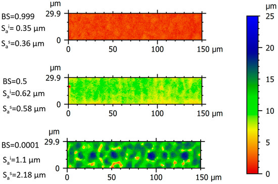
Figure 10.
Roughness and BUMP_SCORE for the bottom plane of a channel. From top to down, three channels with decreasing values of BUMP_SCORE (BS), i.e., increasing presence of irregularities. Roughness values measured from the interferometer (Sai) and computed with the proposed methodology (Sas) are also reported.
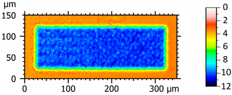
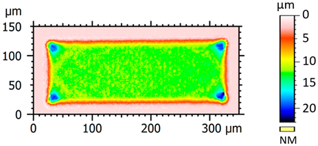
Table 3 presents some numerical analyses of channel bottoms considering depth values (Table 2) derived from the interferometer software MountainsMap 8.2 and the proposed solution based on plane fitting (Section 2.3). The three channels present bumps (a), V-defects at the corners (b), and V-defects within the bottom (c).
Table 3.
Analyses of micro-channel depths and V-defects for three different types of micro-milling works. D is the depth value of the channel, VD is the depth of a V-defect along the channel, and VCD is the depth of a V-defect at corners. Values in μm. The color legend represents the depth.
4. Conclusions
This paper presented a methodology for the quality assessment of micro-machined channels created with a femtosecond laser. The laser beam interacts with the material differently according to the employed parameters (pulse energy, fluence, spot diameter, scanning speed, etc.). Therefore, to optimize the process and production, it is fundamental to have a clear understanding of micro-channel quality as a function of the laser parameters. We have presented an automated process that relies on covariance features and geometric characteristics of micro-channel shapes. Micro-channels are inspected using a white light interferometer, and the created point clouds are automatically analyzed to provide metrics useful for the quality assessment of the micro-milling process. All these automated analyses extract morphological characteristics of micro-channels fundamental for the optimization of the laser process. As the parameter space is very large, the presented automation is very important to support—at the industrial level—the realization of better micro-channels and, more broadly, micro-milling processes. Indeed, the results of the analyses provide sets of laser process parameters that, for example, lead to the generation of bumps or V-defects in a channel of a specific material.
The proposed quality control workflow is replicable also to other activities or applications. It could be implemented directly on the laser platform to monitor the micro-milling process, verifying the absence of defects. As mentioned in the introduction, there is an ongoing effort to apply machine learning algorithms and AI to femtosecond laser processes. However, these approaches require a large amount of data to train the models that are very time-consuming to acquire. The proposed automated workflow can produce large amounts of data with little or no human effort, facilitating the adoption of AI-based optimization strategies by industries. As future work, we are looking into applying machine learning solutions to better optimize the laser processes. It is worth noticing that it could be possible to achieve simultaneous in-situ fabrication and characterization of channels through an integration of the micro-milling system (laser source, scanning device, focusing optics, and motorized stage) and the inspection system (interferometer and motorized stage), assuming the two systems are interoperable.
Author Contributions
Conceptualization, L.C., M.A., E.G. (Eleonora Grilli) and F.R.; methodology, F.B., M.V., L.C., M.A., E.G. (Eleonora Grilli), S.M., R.B., E.G. (Enrico Gallus) and F.R.; formal analysis, F.B., M.V., L.C., M.A., S.M., R.B. and E.G. (Eleonora Grilli); investigation, F.B., M.V., S.M., R.B. and F.M.; resources, E.G. (Enrico Gallus) and F.R.; data curation, F.B., M.V., L.C., M.A., S.M., R.B. and F.M.; writing—original draft preparation, F.B., M.V., L.C., M.A., E.G. (Eleonora Grilli), S.M., R.B., E.G. (Enrico Gallus), F.M. and F.R.; writing—review and editing, M.V. and F.R.; supervision, E.G. (Enrico Gallus) and F.R.; project administration, E.G. (Enrico Gallus) and F.R.; funding acquisition, E.G. (Enrico Gallus) and F.R. All authors have read and agreed to the published version of the manuscript.
Funding
The presented work was supported by the MIAMI project funded by the Autonomous Province of Trento (Italy) within the LP 6/99, art. 5, “Aiuti per la promozione della ricerca e sviluppo” funding schema.
Data Availability Statement
Data are contained within the article.
Conflicts of Interest
No conflict of interest.
References
- Uriarte, L.; Herrero, A.; Ivanov, A.; Oosterling, H.; Staemmler, L.; Tang, P.T.; Allen, D. Comparison between microfabrication technologies for metal tooling. Proc. Inst. Mech.Eng. Part C J. Mech. Eng. Sci. 2006, 220, 1665–1676. [Google Scholar] [CrossRef]
- Câmara, M.A.; Rubio, J.C.; Abrão, A.M.; Davim, J.P. State of the Art on Micromilling of Materials, a Review. J. Mater. Sci. Technol. 2012, 28, 673–685. [Google Scholar] [CrossRef]
- O’Toole, L.; Kang, C.W.; Fang, F.Z. Precision micro-milling process: State of the art. Adv. Manuf. 2021, 9, 173–205. [Google Scholar] [CrossRef]
- Kumar, D.; Singh, N.K.; Bajpai, V. Recent trends, opportunities and other aspects of micro-EDM for advanced manufacturing: A comprehensive review. J. Braz. Soc. Mech. Sci. Eng. 2020, 42, 222. [Google Scholar] [CrossRef]
- Sharma, D.; Hiremath, S.S. Review on tools and tool wear in EDM. Mach. Sci. Technol. 2021, 25, 802–873. [Google Scholar] [CrossRef]
- Bogue, R. Lasers in manufacturing: A review of technologies and applications. Assem. Autom. 2015, 35, 161–165. [Google Scholar] [CrossRef]
- Slusher, R.E. Laser technology. Rev. Mod. Phys. 1999, 71, S471. [Google Scholar] [CrossRef]
- Deepak, J.R.; Anirudh, R.P.; Saran Sundar, S. Applications of lasers in industries and laser welding: A review. Mater. Today Proc. 2023. [Google Scholar] [CrossRef]
- Naresh; Khatak, P. Laser cutting technique: A literature review. Mater. Today Proc. 2022, 56, 2484–2489. [Google Scholar] [CrossRef]
- Gautam, G.D.; Pandey, A.K. Pulsed Nd:YAG laser beam drilling: A review. Opt. Laser Technol. 2018, 100, 183–215. [Google Scholar] [CrossRef]
- Schulz, W.; Eppelt, U.; Poprawe, R. Review on laser drilling I. fundamentals, modeling, and simulation. J. Laser Appl. 2013, 25, 012006. [Google Scholar] [CrossRef]
- Soong, H.K.; Malta, J.B. Femtosecond lasers in ophthalmology. Am. J. Ophthalmol. 2009, 147, 189–197. [Google Scholar] [CrossRef] [PubMed]
- Cvecek, K.; Dehmel, S.; Miyamoto, I.; Schmidt, M. A review on glass welding by ultra-short laser pulses. Int. J. Extrem. Manuf. 2019, 1, 042001. [Google Scholar] [CrossRef]
- Chichkov, B.N.; Momma, C.; Nolte, S.; Von Alvensleben, F.; Tünnermann, A. Femtosecond, picosecond and nanosecond laser ablation of solids. Appl. Phys. 1996, 63, 109–115. [Google Scholar] [CrossRef]
- Gamaly, E.G.; Rode, A.V.; Luther-Davies, B.; Tikhonchuk, V.T. Ablation of solids by femtosecond lasers: Ablation mechanism and ablation thresholds for metals and dielectrics. Phys. Plasmas 2022, 9, 949–957. [Google Scholar] [CrossRef]
- Gamaly, E.G. The physics of ultra-short laser interaction with solids at non-relativistic intensities. Phys. Rep. 2011, 508, 91–243. [Google Scholar] [CrossRef]
- Ahmmed, K.M.T.; Grambow, C.; Kietzig, A.-M. Fabrication of Micro/Nano Structures on Metals by Femtosecond Laser Micromachining. Micromachines 2014, 5, 1219–1253. [Google Scholar] [CrossRef]
- Calabrese, L.; Azzolini, M.; Bassi, F.; Gallus, E.; Bocchi, S.; Maccarini, G.; Pellegrini, G.; Ravasio, C. Micro-Milling Process of Metals: A Comparison between Femtosecond Laser and EDM Techniques. J. Manuf. Mater. Process. 2021, 5, 125. [Google Scholar] [CrossRef]
- Sun, H.; Li, J.; Liu, M.; Yang, D.; Li, F. A Review of Effects of Femtosecond Laser Parameters on Metal Surface Properties. Coatings 2022, 12, 1596. [Google Scholar] [CrossRef]
- Lopez, J.; Niane, S.; Bonamis, G.; Balage, P.; Audouard, E.; Hönninger, C.; Mottay, E.; Manek-Hönninger, I. Percussion drilling in glasses and process dynamics with femtosecond laser GHz-bursts. Opt. Express 2022, 30, 12533–12544. [Google Scholar] [CrossRef]
- Tian, M.; Ma, Z.-C.; Han, Q.; Suo, Q.; Zhang, Z.; Han, B. Emerging applications of femtosecond laser fabrication in neurobiological research. Front. Chem. 2022, 10, 1051061. [Google Scholar] [CrossRef]
- Agarwal, K.; Hatch, K. Femtosecond Laser Assisted Cataract Surgery: A Review. Semin. Ophthalmol. 2021, 36, 618–627. [Google Scholar] [CrossRef]
- Miao, C.; Guo, Z.; Yuan, C. Tribological behavior of co-textured cylinder liner-piston ring during running-in. Friction 2022, 10, 878–890. [Google Scholar] [CrossRef]
- Basbus, J.F.; Cademartori, D.; Asensio, A.M.; Clematis, D.; Savio, L.; Pani, M.; Gallus, E.; Carpanese, M.P.; Barbucci, A.; Presto, S.; et al. Study of a novel microstructured air electrode/electrolyte interface for solid oxide cells. Appl. Surf. Sci. 2024, 652, 159372. [Google Scholar] [CrossRef]
- Reinhold, C.; Pfleging, W. Ultrafast laser structuring of high-voltage cathode materials for lithium-ion batteries. In Laser-Based Micro- and Nanoprocessing XVIII, Proceedings of the SPIE, San Francisco, CA, USA, 29 January–1 February 2024; SPIE: Washington, DC, USA, 2024. [Google Scholar]
- Yang, Y.; Zhao, Y.; Wang, L.; Zhao, Y. Application of femtosecond laser etching in the fabrication of bulk SiC accelerometer. J. Mater. Res. Technol. 2022, 17, 2577–2586. [Google Scholar] [CrossRef]
- Wang, S.; Yang, J.; Deng, G.; Zhou, S. Femtosecond Laser Direct Writing of Flexible Electronic Devices: A Mini Review. Materials 2024, 17, 557. [Google Scholar] [CrossRef]
- Chen, M.-Q.; He, T.-Y.; Zhao, Y. Review of Femtosecond Laser Machining Technologies for Optical Fiber Microstructures Fabrication. Opt. Laser Technol. 2022, 147, 107628. [Google Scholar] [CrossRef]
- Wang, B.; Wang, P.; Song, J.; Lam, Y.C.; Song, H.; Wang, Y.; Liu, S. A hybrid machine learning approach to determine the optimal processing window in femtosecond laser-induced periodic nanostructures. J. Mater. Process. Technol. 2022, 308, 117716. [Google Scholar] [CrossRef]
- Mills, B.; Grant-Jacob, J.A. Lasers that learn: The interface of laser machining and machine learning. IET Optoelectron. 2021, 15, 207–224. [Google Scholar] [CrossRef]
- Mottay, E.P. Comparison and optimization of analytical and small dataset machine learning models for laser micro-processing. In Laser-Based Micro- and Nanoprocessing XVIII, Proceedings of the SPIE, San Francisco, CA, USA, 29 January–1 February 2024; SPIE: Washington, DC, USA, 2024. [Google Scholar]
- Yoshitomi, D.; Takada, H.; Miyoshi, T.; Nagai, D.; Miyaji, G.; Narazaki, A. Data-driven ultrashort pulse laser processing using deep neural network for shape prediction and in-process monitoring. In Frontiers in Ultrafast Optics: Biomedical, Scientific, and Industrial Applications XXIV, Proceedings of the SPIE, San Francisco, CA, USA, 28–30 January 2024; SPIE: Washington, DC, USA, 2024. [Google Scholar]
- Prakash, S.; Kumar, S. Fabrication of microchannels: A review. Proc. Inst. Mech.Eng. Part B J. Eng. Manuf. 2015, 229, 1273–1288. [Google Scholar] [CrossRef]
- Bauer, F.; Michalowski, A.; Kiedrowski, T.; Nolte, S. Heat accumulation in ultra-short pulsed scanning laser ablation of metals. Opt. Express 2015, 23, 1035–1043. [Google Scholar] [CrossRef] [PubMed]
- Schille, J.; Schneider, L.; Loeschner, U.; Ebert, R.; Scully, P.; Goddard, N.; Steiger, B.; Exner, H. Micro processing of metals using a high repetition rate femtosecond laser: From laser process parameter study to machining examples. In Proceedings of the 30th International Congress on Laser Materials Processing, Laser Microprocessing and Nanomanufacturing, Orlando, FL, USA, 23–27 October 2011. [Google Scholar]
- Chehata, N.; Guo, L.; Mallet, C. Airborne lidar feature selection urban classification using random forests. Int. Arch. Photogramm. Remote Sens. Spat. Inf. Sci. 2009, 38, 207–212. [Google Scholar]
- Rodríguez-Gonzálvez, P.; Jiménez Fernández-Palacios, B. Point cloud optimization based on 3D geometric features for architectural heritage modelling. DISEGNARECON 2021, 14, 18.1–18.9. [Google Scholar]
- dos Santos, R.C.; Galo, M.; Habib, A.F. K-means clustering based on omnivariance attribute for building detection from airborne LiDAR data. ISPRS Ann. Photogramm. Remote Sens. Spat. Inf. Sci. 2022, 2, 111–118. [Google Scholar] [CrossRef]
- Niemeyer, J.; Rottensteiner, F.; Soergel, U. Contextual classification of LiDAR data and building object detection in urban areas. ISPRS J. Photogramm. Remote Sens. 2014, 87, 152–165. [Google Scholar] [CrossRef]
- Weinmann, M.; Jutzi, B.; Mallet, C.; Weinmann, M. Geometric features and their relevance for 3d point cloud classification. ISPRS Ann. Photogramm. Remote Sens. Spat. Inf. Sci. 2017, IV-1-W1, 157–164. [Google Scholar] [CrossRef]
- Grilli, E.; Farella, E.M.; Torresani, A.; Remondino, F. Geometric features analysis for the classification of cultural heritage point clouds. Int. Arch. Photogramm. Remote Sens. Spat. Inf. Sci. 2019, XLII-2/W15, 541–548. [Google Scholar] [CrossRef]
- Blomley, R.; Weinmann, M.; Leitloff, J.; Jutzi, B. Shape distribution features for point cloud analysis—A geometric histogram approach on multiple scales. ISPRS Ann. Photogramm. Remote Sens. Spat. Inf. Sci. 2014, II-3, 9–16. [Google Scholar] [CrossRef]
Disclaimer/Publisher’s Note: The statements, opinions and data contained in all publications are solely those of the individual author(s) and contributor(s) and not of MDPI and/or the editor(s). MDPI and/or the editor(s) disclaim responsibility for any injury to people or property resulting from any ideas, methods, instructions or products referred to in the content. |
© 2024 by the authors. Licensee MDPI, Basel, Switzerland. This article is an open access article distributed under the terms and conditions of the Creative Commons Attribution (CC BY) license (https://creativecommons.org/licenses/by/4.0/).